

STMicroelectronics M95M04-DR Datasheet
SO8N (MN)
150 mil width
TSSOP8 (DW)
169 mil width
WLCSP (2.809 × 1.863 mm)
Product status link
M95M04-DR
M95M04-DR
Datasheet
4-Mbit serial SPI bus EEPROM
Features
• Compatible with the serial peripheral interface (SPI) bus
• Memory array
– 4 Mbit (512 Kbytes) of EEPROM
– Page size: 512 bytes
– Additional write lockable page (identification page)
• Write time
– Byte write within 5 ms
– Page write within 5 ms
• Write protect
– quarter array
– half array
– whole memory array
• Max clock frequency:
– 10 MHz for VCC ≥ 2.5 V
– 5 MHz for VCC ≥ 1.8 V
• Single supply voltage: 1.8 V to 5.5 V
• Operating temperature range: from -40 °C up to +85 °C
• Enhanced ESD protection (up to 4 kV in human body model)
• More than 4 million write cycles
• More than 40-year data retention
• Packages
– SO8N (ECOPACK2)
– TSSOP8 (ECOPACK2)
– WLCSP (ECOPACK2)
DS12179 - Rev 2 - February 2021
For further information contact your local STMicroelectronics sales office.
www.st.com
1 Description
The M95M04-DR device is electrically erasable programmable memory (EEPROM) organized as 524288 x 8 bits,
accessed through the SPI bus.
The M95M04-DR can operate with a supply range from 1.8 to 5.5 V, and is guaranteed over the -40 °C/+85 °C
temperature range.
The M95M04-DR offer an additional page, named the identification page (512 bytes). The identification page can
be used to store sensitive application parameters that can be (later) permanently locked in read-only mode.
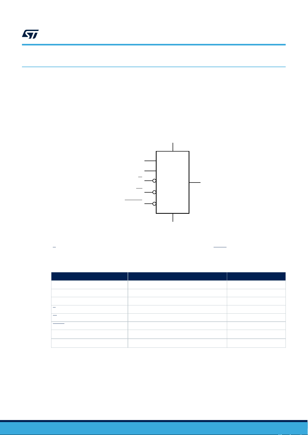
Figure 1. Logic diagram
V
CC
D
C
M95M04-DR
Description
S
M95xxx
Q
W
HOLD
V
SS
The SPI bus signals are C, D and Q, as shown in Figure 1 and Table 1. The device is selected when Chip select
(S) is driven low. Communications with the device can be interrupted when the HOLD is driven low.
Table 1. Signal names
Signal name
C Serial clock Input
D Serial data input Input
Q Serial data output Output
S Chip select Input
W Write protect Input
HOLD Hold Input
V
CC
V
SS
Supply voltage -
Ground -
Function Direction
MS45413V1
DS12179 - Rev 2
page 2/44
Figure 2. 8-pin package connections (top view)
M95xxx
S V
1
8
CC
M95M04-DR
Description
2
W
3
4
SS
1. See Section 10 Package information for package dimensions, and how to identify pin 1.
Figure 3. WLCSP connections
4 3 2 1
A
B
C
HOLDQ
7
C
6
DV
5
MS51579V1
1 2 3 4
A
B
C
D
Bump side view
Table 2. Signals vs. bump position
Position
1 - - C -
2
3 S - -
4 - Q W -
A B C D
V
CC
D
Top view (bumps underneath)
HOLD - D
MS38243V1
V
SS
DS12179 - Rev 2
page 3/44
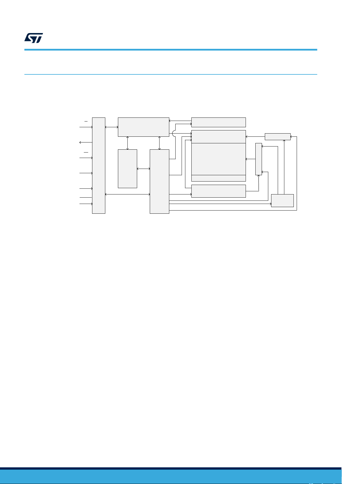
2 Memory organization
The memory is organized as shown in the following figure.
M95M04-DR
Memory organization
Figure 4. Block diagram
S
Q
W
D
C
HOLD
I/Os
Data register and ECC
Status
register
Control
logic
Sense amplifiers
Page latches
Array
Custom area
HV generator
and sequencer
X decoder
Y decoder
Address
register
MS52059V1
DS12179 - Rev 2
page 4/44

3 Signal description
During all operations, VCC must be held stable and within the specified valid range: VCC(min) to VCC(max).
All of the input and output signals must be held high or low (according to voltages of VIH, VOH, VIL or VOL, as
specified in Section 9 DC and AC parameters). These signals are described next.
M95M04-DR
Signal description
3.1
Serial data output (Q)
This output signal is used to transfer data serially out of the device. Data is shifted out on the falling edge of serial
clock (C).
3.2 Serial data input (D)
This input signal is used to transfer data serially into the device. It receives instructions, addresses, and the data
to be written. Values are latched on the rising edge of serial clock (C).
3.3 Serial clock (C)
This input signal provides the timing of the serial interface. Instructions, addresses, or data present at serial data
input (D) are latched on the rising edge of serial clock (C). Data on serial data output (Q) change from the falling
edge of serial clock (C).
3.4 Chip select (S)
When this input signal is high, the device is deselected and serial data output (Q) is at high impedance. The
device is in the standby power mode, unless an internal write cycle is in progress. Driving chip select (S) low
selects the device, placing it in the active power mode.
After power-up, a falling edge on chip select (S) is required prior to the start of any instruction.
3.5 Hold (HOLD)
The hold (HOLD) signal is used to pause any serial communications with the device without deselecting the
device.
During the hold condition, the serial data output (Q) is high impedance, and serial data input (D) and serial clock
(C) are "Don’t care".
To start the hold condition, the device must be selected, with chip select (
S) driven low.
3.6 Write protect (W)
The main purpose of this input signal is to freeze the size of the area of memory that is protected against Write
instructions (as specified by the values in the BP1 and BP0 bits of the Status register).
This pin must be driven either high or low, and must be stable during all Write instructions.
3.7 V
supply voltage
CC
VCC is the supply voltage.
3.8 VSS ground
VSS is the reference for all signals, including the VCC supply voltage.
DS12179 - Rev 2
page 5/44
4 Connecting to the SPI bus
All instructions, addresses and input data bytes are shifted in to the device, most significant bit first. The serial
data input (D) is sampled on the first rising edge of the serial clock (C) after chip select (S) goes low.
All output data bytes are shifted out of the device, most significant bit first. The serial data output (Q) is latched
on the first falling edge of the serial clock (C) after the instruction (such as the read from memory array and read
status register instructions) have been clocked into the device.
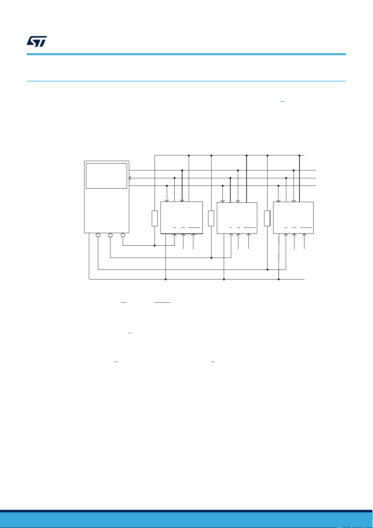
Figure 5. Bus master and memory devices on the SPI bus
M95M04-DR
Connecting to the SPI bus
V
CC
SPI interface with
(CPOL, CPHA) =
(0, 0) or 1, 1)
SPI bus master
CS3 CS2 CS1
SDO
SDI
SCK
V
CC
SPI memory
R R R
device
S
W
HOLD
(1) (1) (1) (1) (1) (1)
SPI memory
device
S
W
V
CC
HOLD
C Q DC Q DC Q D
SPI memory
device
S
W
V
CC
HOLD
V
MS19755V3
SS
1. The write protect (W) and hold (HOLD) signals should be driven, high or low as appropriate.
Figure 5 shows an example of three memory devices connected to an SPI bus master. Only one memory device
is selected at a given time, so only one memory device drives the serial data output (Q) line at that time. The
other memory devices are in high impedance state. The pull-up resistor R ensures that a device is not selected if
the bus master leaves the
S line in the high impedance state.
In applications where the bus master may leave all SPI bus lines in high impedance at the same time (for
example, if the Bus master is reset during the transmission of an instruction), it is recommended to connect the
clock line (C) to an external pull-down resistor so that, if all inputs/outputs become high impedance, the C line is
pulled low (while the
so, that the t
SHCH
S line is pulled high): this ensures that S and C do not become high at the same time, and
requirement is met. The typical value of R is 100 kΩ.
DS12179 - Rev 2
page 6/44
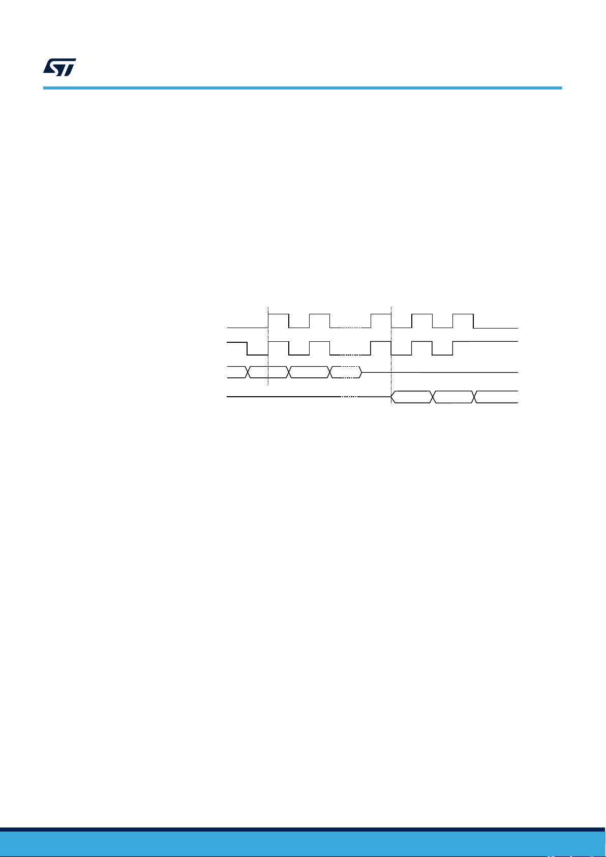
4.1 SPI modes
These devices can be driven by a microcontroller with its SPI peripheral running in either of the following two
modes:
• CPOL = 0, CPHA = 0
• CPOL = 1, CPHA = 1
For these two modes, input data is latched in on the rising edge of serial clock (C), and output data is available
from the falling edge of serial clock (C).
The difference between the two modes, as shown in Figure 6, is the clock polarity when the bus master is in
stand-by mode and not transferring data:
• C remains at 0 for (CPOL = 0, CPHA = 0)
• C remains at 1 for (CPOL = 1, CPHA = 1)
M95M04-DR
SPI modes
Figure 6. SPI modes supported
CPOL
0
1
CPHA
0
1
C
C
D
Q
MSB
MSB
MS42674V2
DS12179 - Rev 2
page 7/44

5 Operating features
5.1 Supply voltage (VCC)
5.1.1 Operating supply voltage (VCC)
Prior to selecting the memory and issuing instructions to it, a valid and stable VCC voltage within the specified
[VCC(min), VCC(max)] range must be applied (see operating conditions in Section 9 DC and AC parameters).
This voltage must remain stable and valid until the end of the transmission of the instruction and, for a Write
instruction, until the completion of the internal write cycle (tW). In order to secure a stable DC supply voltage, it is
recommended to decouple the VCC line with a suitable capacitor (usually in the range between 10 and 100 nF)
close to the VCC / VSS device pins.
5.1.2 Device reset
In order to prevent erroneous instruction decoding and inadvertent write operations during power-up, a power-onreset (POR) circuit is included. At power-up, the device does not respond to any instruction until VCC reaches the
POR threshold voltage. This threshold is lower than the minimum VCC operating voltage (see operating conditions
in Section 9 DC and AC parameters).
At power-up, when VCC passes over the POR threshold, the device is reset and is in the following state:
• in Standby power mode,
• deselected,
• Status register values:
– the write enable latch (WEL) bit is reset to 0
– the write in progress (WIP) bit is reset to 0
– the SRWD, BP1 and BP0 bits remain unchanged (non-volatile bits).
It is important to note that the device must not be accessed until VCC reaches a valid and stable level within
the specified [VCC(min), VCC(max)] range, as defined under Operating conditions in Section 9 DC and AC
parameters.
M95M04-DR
Operating features
5.1.3 Power-up conditions
When the power supply is turned on, VCC rises continuously from VSS to VCC. During this time, the chip select (S)
line is not allowed to float but should follow the VCC voltage. It is therefore recommended to connect the
VCC via a suitable pull-up resistor (see Figure 5).
In addition, the chip select (S) input offers a built-in safety feature, as the S input is edge-sensitive as well as
level-sensitive: after power-up, the device does not become selected until a falling edge has first been detected
on chip select (
operation.
The VCC voltage has to rise continuously from 0 V up to the minimum VCC operating voltage defined in
Section 9 DC and AC parameters.
S). This ensures that chip select (S) must have been high, prior to going low to start the first
S line to
DS12179 - Rev 2
page 8/44
M95M04-DR
Active power and standby power modes
5.1.4 Power-down
During power-down (continuous decrease of the VCC supply voltage below the minimum VCC operating voltage
defined in Section 9 DC and AC parameters), the device must be:
• deselected (chip select
• in standby power mode (there must not be any internal write cycle in progress).
S must be allowed to follow the voltage applied on VCC)
5.2 Active power and standby power modes
When chip select (S) is low, the device is selected, and in the active power mode. The device consumes ICC.
When chip select (S) is high, the device is deselected. If a write cycle is not currently in progress, the device then
goes into the standby power mode, and the device consumption drops to I
(see Section 9 DC and AC parameters).
, as specified in DC characteristics
CC1
5.3 Hold condition
The hold (HOLD) signal is used to pause any serial communications with the device without resetting the clocking
sequence.
To enter the hold condition, the device must be selected, with chip select (S) low.
During the hold condition, the serial data output (Q) is high impedance, and the serial data input (D) and the serial
clock (C) are "Don’t care".
Normally, the device is kept selected for the whole duration of the Hold condition. Deselecting the device while it is
in the hold condition has the effect of resetting the state of the device: this mechanism can be used, if required, to
reset the ongoing processes.
Note: This resets the internal logic, except the WEL and WIP bits of the status register.
Note: In the specific case where the device has moved in a write command (Inst + Address + data bytes, each data
byte being exactly 8 bits), deselecting the device also triggers the write cycle of this decoded command.
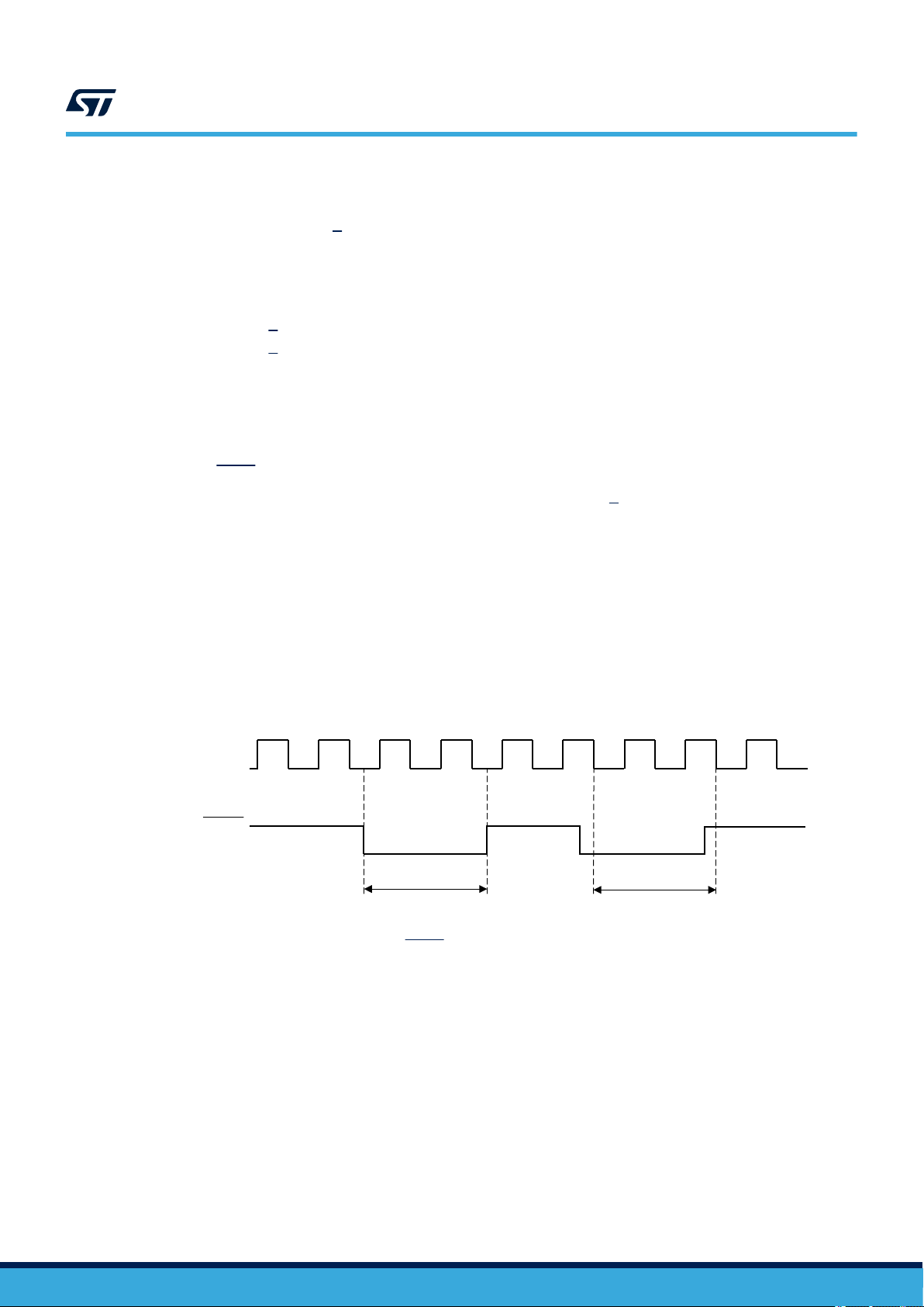
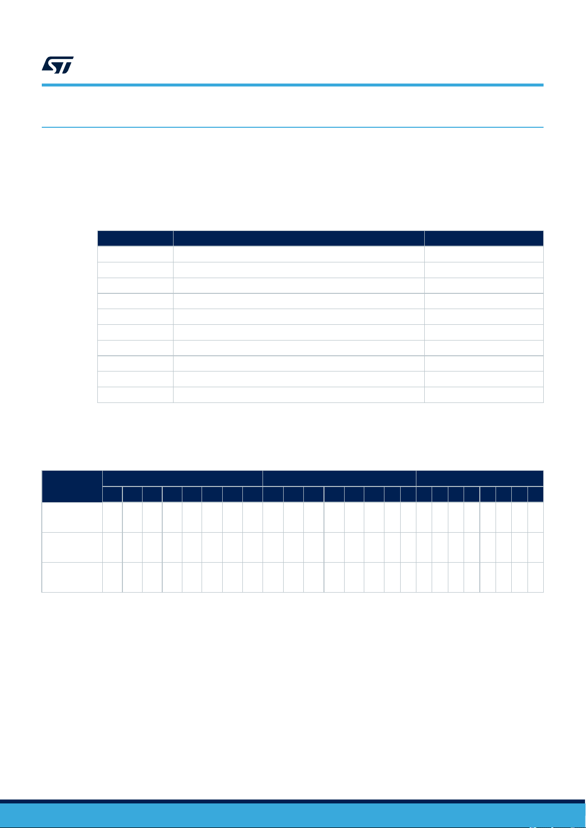
Figure 7. Hold condition activation
C
HOLD
Hold
condition
The hold condition starts when the hold (HOLD) signal is driven low when serial clock (C) is already low (as
shown in Figure 7).
Figure 7 also shows what happens if the rising and falling edges are not timed to coincide with serial clock (C)
being low.
Hold
condition
MS47281V1
DS12179 - Rev 2
page 9/44
5.4 Status register
The status register contains a number of status and control bits that can be read or set (as appropriate) by
specific instructions. See Section 6.3 Read status register (RDSR) for a detailed description of the status register
bits.
5.5 Data protection and protocol control
The device features the following data protection mechanisms:
• Before accepting the execution of the write and write status register instructions, the device checks whether
the number of clock pulses comprised in the instructions is a multiple of eight.
• All instructions that modify data must be preceded by a write enable (WREN) instruction to set the write
enable latch (WEL) bit.
• The block protect (BP1, BP0) bits in the status register are used to configure part of the memory as
read-only.
• The write protect (
For any instruction to be accepted, and executed, chip select (
serial clock (C) for the last bit of the instruction, and before the next rising edge of serial clock (C).
Two points to note in the previous sentence:
• The “last bit of the instruction” can be the eighth bit of the instruction code, or the eighth bit of a data byte,
depending on the instruction (except for read status register (RDSR) and read (READ) instructions).
• The “next rising edge of serial clock (C)” might (or might not) be the next bus transaction for some other
device on the SPI bus.
W) signal is used to protect the block protect (BP1, BP0) bits in the status register.
M95M04-DR
Status register
S) must be driven high after the rising edge of
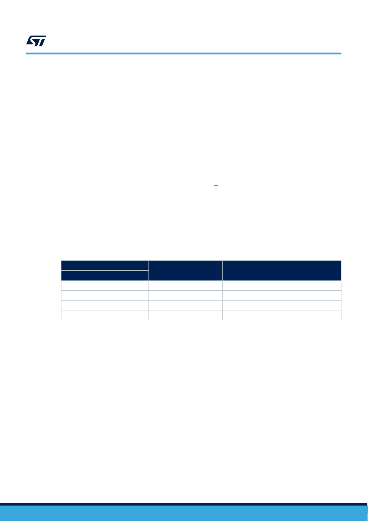
Table 3. Write-protected block size
Status register bits
BP1 BP0
0 0
0 1 Upper quarter 60000h - 7FFFFh
1 0 Upper half 40000h - 7FFFFh
1 1 Whole memory 00000h - 7FFFFh
Protected block Protected array addresses
None None
DS12179 - Rev 2
page 10/44
6 Instructions
Each command is composed of bytes (MSB bit transmitted first), initiated with the instruction byte, as summarized
in Table 4.
If an invalid instruction is sent (one not contained in Table 4), the device automatically enters in a wait state until
deselected.
Instruction Description Instruction format
WREN Write enable 0000 0110
WRDI Write disable 0000 0100
RDSR Read status register 0000 0101
WRSR Write status register 0000 0001
READ Read from memory array 0000 0011
WRITE Write to memory array 0000 0010
RDID Read identification page 1000 0011
WRID Write identification page 1000 0010
RDLS Read identification page lock status 1000 0011
LID Lock identification page in react-only mode 1000 0010
M95M04-DR
Instructions
Table 4. Instruction set
For read and write commands to memory array and identification page the address is defined by three bytes as
explained in Table 5.
Instruction
READ
or WRITE
RDID
or WRID
RDLS
or LID
1. A: Significant address bit
2. X: Don't Care bit
(1)(2)
b23 b22 b21 b20 b19 b18 b17 b16 b15 b14 b13 b12 b11 b10 b9 b8 b7 b6 b5 b4 b3 b2 b1 b0
X X X X X A18 A17 A16 A15 A14 A13 A12 A11 A10 A9 A8 A7 A6 A5 A4 A3 A2 A1 A0
X X X X X X X X X X X X X 0 X A8 A7 A6 A5 A4 A3 A2 A1 A0
X X X X X X X X X X X X X 1 X X X X X X X X X X
Table 5. Significant bits within the address bytes
Upper address byte Middle address byte Lower address byte
DS12179 - Rev 2
page 11/44
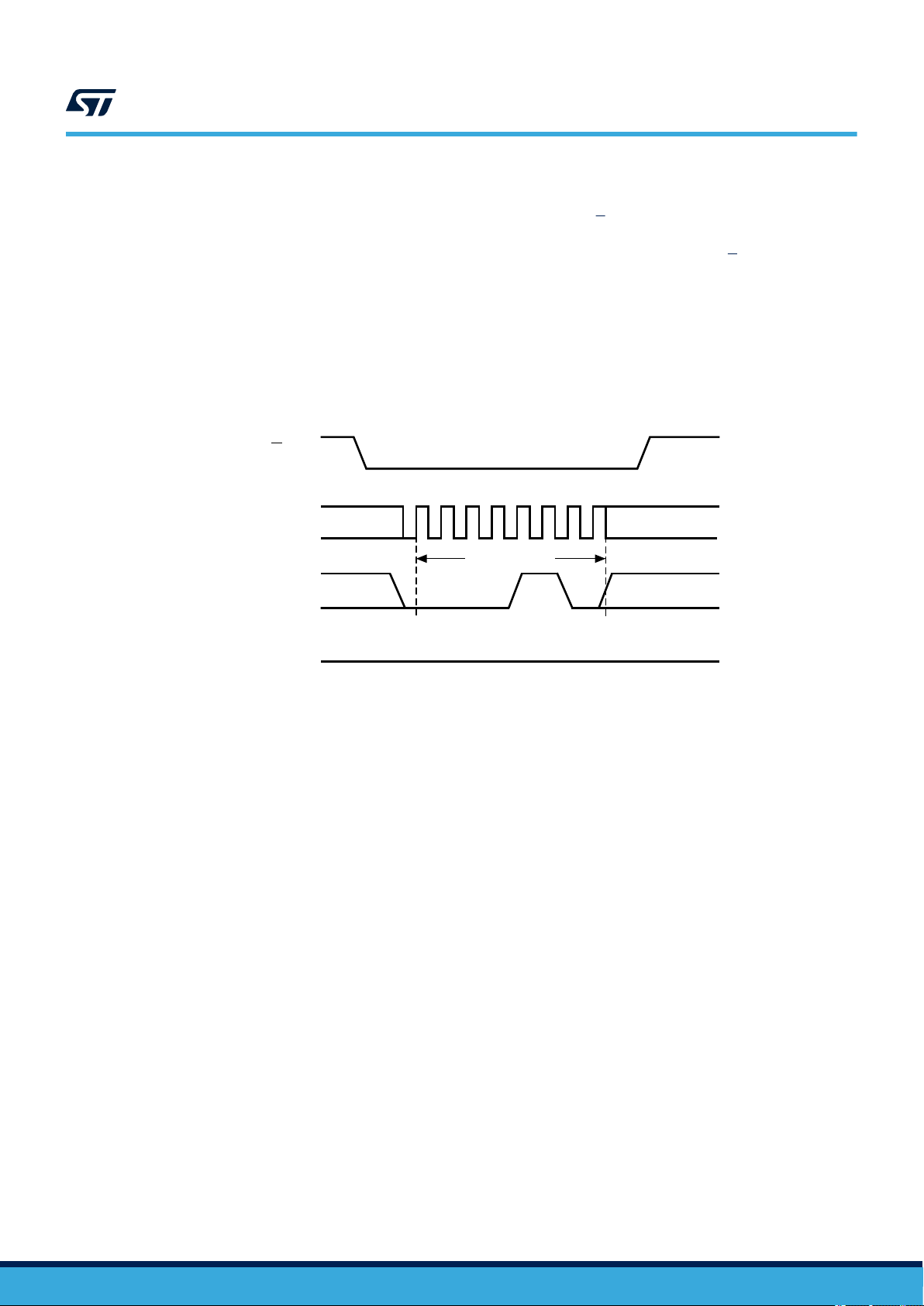
6.1 Write enable (WREN)
The write enable latch (WEL) bit must be set prior to each WRITE and WRSR instruction. The only way to do this
is to send a write enable instruction to the device.
As shown in Figure 8, to send this instruction to the device, chip select (S) is driven low, and the bits of the
instruction byte are shifted in, on serial data input (D). The device then enters a wait state. It waits for the device
to be deselected by chip select (S) being driven high.
S
M95M04-DR
Write enable (WREN)
Figure 8. Write enable (WREN) sequence
C
D
Q
0
21 3 4 5 6 7
Instruction
High impedance
MS41478V1
DS12179 - Rev 2
page 12/44
6.2 Write disable (WRDI)
One way of resetting the write enable latch (WEL) bit is to send a write disable instruction to the device.
As shown in Figure 9, to send this instruction to the device, chip select (S) is driven low, and the bits of the
instruction byte are shifted in, on serial data input (D).
The device then enters a wait state. It waits for a the device to be deselected, by chip select (S) being driven high.
The write enable latch (WEL) bit, in fact, becomes reset by any of the following events:
• Power-up
• WRDI instruction execution
• WRSR instruction completion
• WRITE instruction completion.
S
M95M04-DR
Write disable (WRDI)
Figure 9. Write disable (WRDI) sequence
C
D
Q
0
21 3 4 5 6 7
Instruction
High impedance
MS41478V1
DS12179 - Rev 2
page 13/44
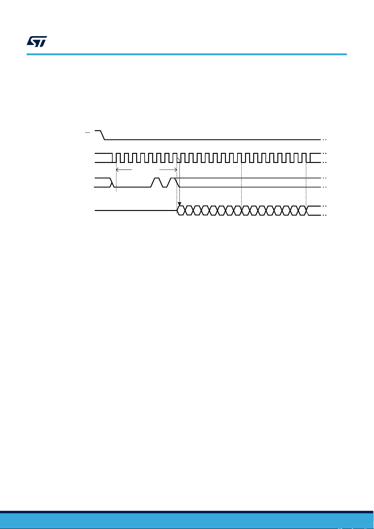
6.3 Read status register (RDSR)
The read status register (RDSR) instruction is used to read the status register. The status register may be read at
any time, even while a write or write status register cycle is in progress. When one of these cycles is in progress,
it is recommended to check the write in progress (WIP) bit before sending a new instruction to the device. It is
also possible to read the Status register continuously, as shown in Figure 10.
Figure 10. Read Status register (RDSR) sequence
S
21 3 4 5 6 7 8 9 10 11 12 13 14 15
0
C
Instruction
D
M95M04-DR
Read status register (RDSR)
The status and control bits of the status register are detailed in the following subsections.
6.3.1 WIP bit
The WIP bit (write in progress) is a read-only flag that indicates the ready/busy state of the device. When a write
command (WRITE, WRSR, WRID, LID) has been decoded and a write cycle (tW) is in progress, the device is
busy and the WIP bit is set to 1. When WIP = 0 the device is ready to decode a new command.
During a write cycle, reading continuously the WIP bit allows to detect when the device becomes ready (WIP = 0)
to decode a new command.
6.3.2 WEL bit
The WEL bit (write enable latch) bit is a flag that indicates the status of the internal write enable latch. When WEL
is set to 1, the write instructions (WRITE, WRSR, WRID, LID) are executed; when WEL is set to 0, any decoded
write instruction is not executed.
The WEL bit is set to 1 with the WREN instruction. The WEL bit is reset to 0 after the following events:
• Write disable (WRDI) instruction completion
• Write instructions (WRITE, WRSR, WRID, LID) completion including the write cycle time t
• Power-up
High impedance
Status Register Out
Q
MSB MSB
Status Register Out
77 6 5 4 3 2 1 0 7 6 5 4 3 2 1 0
MS47548V1
W
6.3.3 BP1, BP0 bits
The block protect (BP1, BP0) bits are non volatile. They define the size of the area to be software-protected
against Write instructions. These bits are written with the write status register (WRSR) instruction. When one or
both of the block protect (BP1, BP0) bits is set to 1, the relevant memory area (as defined in Table 3) becomes
protected against write (WRITE) instructions. The block protect (BP1, BP0) bits can be written provided that the
hardware protected mode has not been set.
DS12179 - Rev 2
page 14/44
 Loading...