

Page 1
5.0V, 16 Kbit (2Kb x 8) TIMEKEEPER®SRAM
FEATURES SUMMARY
■ INTEGRATED, ULTRA LOW POWER SRAM,
REAL TIME CLOCK,and POWER-FAIL
CONTROL CIRCUIT
■ BYTEWIDE™ RAM-LIKE CLOCK ACCESS
■ BCD CODED YEAR, MONTH, DAY, DATE,
HOURS, MINUTES, and SE CONDS
■ TYPICAL CLOCK ACCURACY OF ±1 MINUTE
A MONTH, A T 25°C
■ SOFTWARE CONTROLLED CLOCK
CALIBRATION FOR HIGH ACCURACY
APPLICATIONS
■ AUTOMATIC POWER-FAIL CHIP DESELECT
and WRITE PROTECTION
■ WRITE PROTECT VOLTAGES
= Power-fail Deselect V oltage):
(V
PFD
– M48T02: V
4.5V ≤ V
– M48T12: V
4.2V ≤ V
■ SELF-CONTAINED BATTERYandCRYSTAL
IN T HE CAPHAT™ DIP PACKAGE
■ PIN and FUNCTION COMPATIBLE WITH
JEDEC STANDARD 2K x 8 SRAMs
= 4.75 to 5.5V
CC
≤ 4.75V
PFD
= 4.5 to 5.5V
CC
≤ 4.5V
PFD
M48T02
M48T12
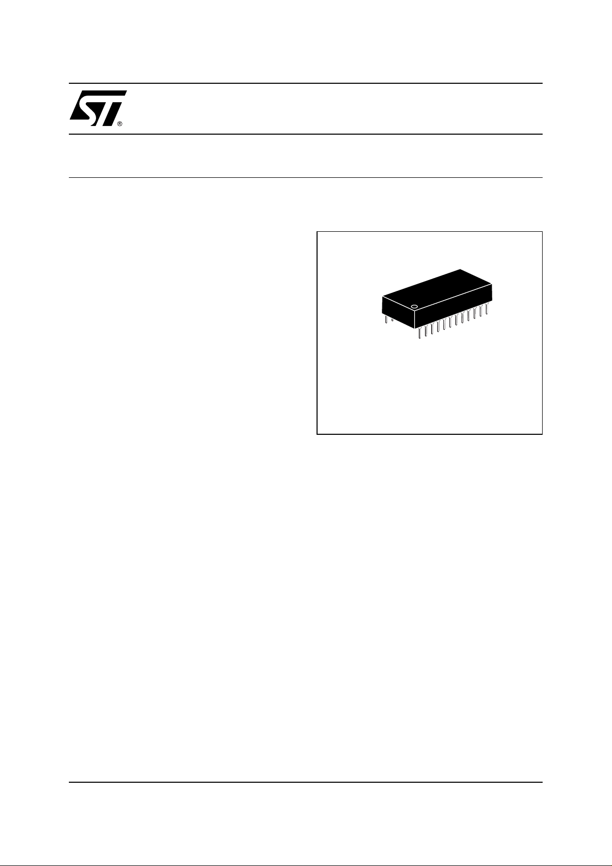
Figure 1. 24-pin P CDI P, CAPHAT™ Package
24
1
PCDIP24 (PC)
Battery/Crystal
CAPHAT
1/19May 2002
Page 2

M48T02, M48T12
TABLE OF CONTENTS
SUMMARYDESCRIPTION...........................................................3
LogicDiagram(Figure2.).........................................................3
SignalNames(Table1.)..........................................................3
DIP Connect ions (Figure 3.) .......................................................3
BlockDiagram(Figure4.).........................................................4
MAXIMUMRATING.................................................................4
AbsoluteMaximumRatings(Table2.) ...............................................4
DC AND AC PARAMETERS. . ........................................................5
Operating and AC Measurement Conditions (Table 3.) ..................................5
AC Testing Load Circuit (Figure 5.)..................................................5
Capacitance (Table 4. ) . . . ........................................................5
DCCharacteristics(Table5.) ......................................................6
OPERATIONMODES...............................................................6
Operating Modes (Table 6.)........................................................6
READMode....................................................................7
READModeACWaveforms(Figure6.)..............................................7
READModeACCharacteristics(Table7.)............................................7
WRITEMode...................................................................8
WRITE Enable Controlled, WRITE AC Waveform (Figure 7.)..............................8
ChipEnableControlled,WRITEACWaveforms(Figure8.)...............................8
WRITEModeACCharacteristics(Table8.)...........................................9
DataRetentionMode............................................................10
CheckingtheBOKFlagStatus(Figure9.) ...........................................10
PowerDown/UpModeACWaveforms(Figure10.)....................................11
PowerDown/UpACCharacteristics(Table9.)........................................11
PowerDown/UpTripPointsDCCharacteristics(Table10.)..............................11
CLOCKOPERATIONS.............................................................12
Reading the Clock . .............................................................12
SettingtheClock...............................................................12
RegisterMap(Table11.).........................................................12
Stopping and S tarting the Oscillator ................................................13
CalibratingtheClock............................................................13
CrystalAccuracyAcrossTemperature(Figure11.) ....................................14
ClockCalibration(Figure12.).....................................................14
V
Noise And Negative Going Transients. ..........................................15
CC
SupplyVoltageProtection(Figure13.)..............................................15
PARTNUMBERING ...............................................................16
PACKAGE MECHANICAL INFORMATION . . . ..........................................17
REVISIONHISTORY...............................................................18
2/19
Page 3
M48T02, M48T12
SUMMARY DESCRIPTION
®
TheM48T02/12TIMEKEEPER
RAM is a 2Kb x 8
non-volatile sta tic RAM and real time clock which
is pin and f unctional compatible with the DS1642.
A special 24-pin, 600mil DIP CAP HAT™ package
houses the M48T02/12 silicon with a quartz cryst al
and a long life lithium button cell to form a highly
integrated battery back ed-up m emory an d real
time clock solution.
The M48T02/12 button cell has sufficient capacity
and storage life to maintain data and clock func-
tionality for an accum ulat ed time period of at least
10 years in the absence of power over the operating temperature range.
The M48T02/12 is a non-volatile pin and function
equivalent to any JEDEC standard 2Kb x 8 SRAM.
It also easily fits into many ROM, EPROM, and
EEPROM sockets, providing the non-volatility of
PROMs without any requirement for special
WRITE timing or limitations on the number of
WRITEs that can be performed.
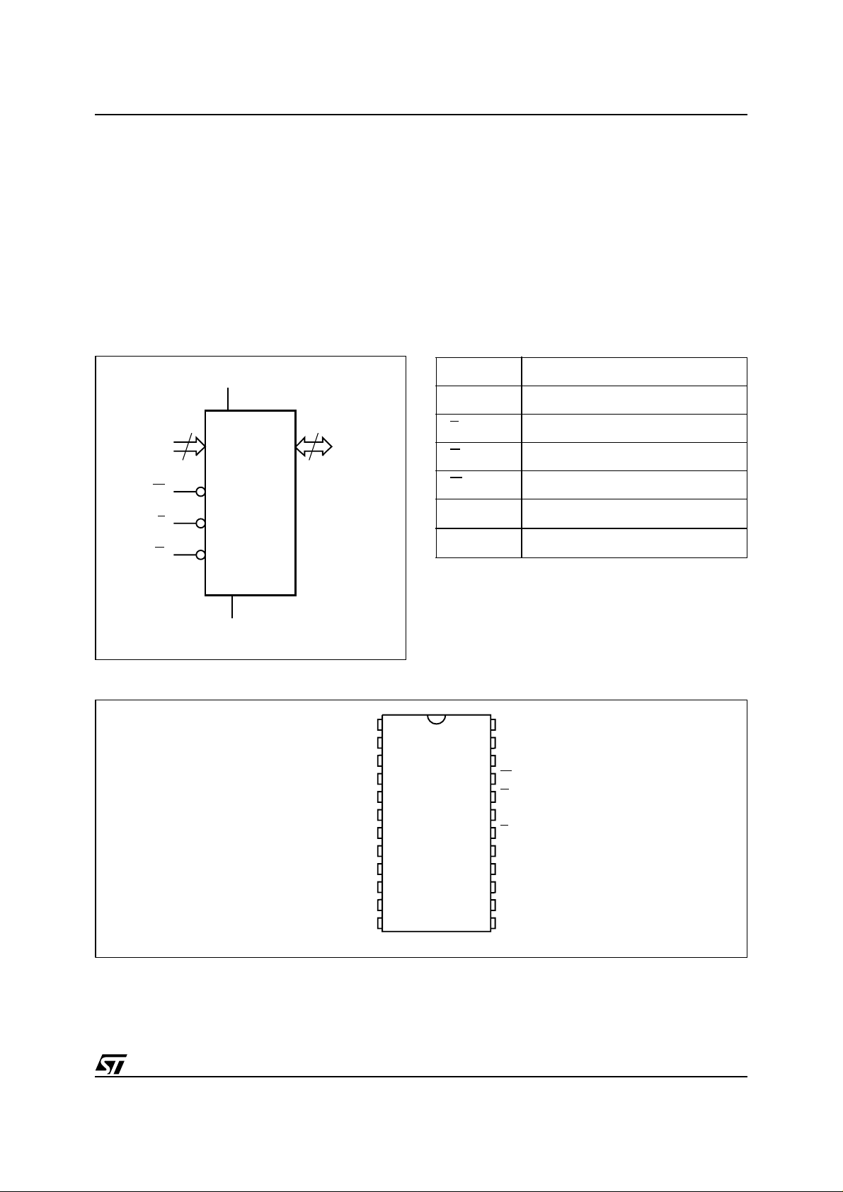
Figure 2. Logic Diagram Table 1. Signal Names
A0-A10 Address Inputs
DQ0-DQ7 Data Inputs / Outputs
E
G
W
V
V
CC
SS
Chip Enable
Output Enable
WRITE Enable
Supply Voltage
Ground
A0-A10
W
V
CC
11
M48T02
M48T12
E
G
8
DQ0-DQ7
V
SS
Figure 3. DIP Connections
AI01027
A7
A6
A5
A4
A3
A2
A1
A0
DQ0
DQ2
SS
1
2
3
4
5
6
7
8
9
10
11
12
M48T02
M48T12
24
23
22
21
20
19
18
17
16
15
14
13
AI01028
V
CC
A8
A9
W
G
A10
E
DQ7
DQ6
DQ5DQ1
DQ4
DQ3V
3/19
Page 4
M48T02, M48T12
Figure 4. Block Diagram
OSCILLATOR AND
CLOCK CHAIN
32,768 Hz
CRYSTAL
POWER
LITHIUM
CELL
VOLTAGE SENSE
AND
SWITCHING
CIRCUITRY
V
CC
MAXIMUM RATING
Stressingthedeviceabovetheratinglistedinthe
“Absolute Maximum Ratings” table may c ause
permanent damage to the dev ice. These are
stress ratings only and operation of the device at
these or any other conditions a bove those indicated in the Ope ratin g sections of this specification is
8 x 8 BiPORT
SRAM ARRAY
A0-A10
DQ0-DQ7
E
W
G
AI01329
V
PFD
BOK
2040 x 8
SRAM ARRAY
V
SS
not implied. Expos ure to Absolute Max imum Rating c ondit ions for extended periods may affect device reliability. Refer also to the
STMicroelectronics SURE Program and other relevant quality documents.
Table 2. Absolute Maximum Ratings
Symbol Parameter Value Unit
T
A
T
STG
(2)
T
SLD
V
IO
V
CC
I
O
P
D
Note: 1. Soldering temperature not to exceed 260°C for 10 seconds (total thermal budget not to exceed 150°C for longer than 30 seconds).
CAUTION: Negative undershoots below –0.3V are not allowed on any pin while in the Battery Back-up mode.
4/19
Ambient Operating Temperature 0 to 70 °C
Storage Temperature (VCCOff, Oscillator Off)
–40 to 85 °C
Lead Solder Temperature for 10 seconds 260 °C
Input or Output Voltages –0.3 to 7 V
Supply Voltage –0.3 to 7 V
Output Current 20 mA
Power Dissipation 1 W
Page 5
DC AND AC PARAMETERS
This s ec t ion summarizes the operating and measurement conditions, as well as the DC and AC
characteristics of the device. The parameters in
the following DC and AC Charact eristic tables are
derived from tests performed under the Measure-
Table 3. Operating and AC Measu rement Conditions
Parameter M48T02 M48T12 Unit
M48T02, M48T12
ment Conditions listed in the relevant tables. Designers should check that the operating conditions
in their projects match the measure ment conditions when using t he quoted parameters.
Supply Voltage (V
Ambient Operating Temperature (T
Load Capacitance (C
CC
)
)
A
)
L
4.75 to 5.5 4.5 to 5.5 V
0 to 70 0 to 70 °C
100 100 pF
Input Rise and Fall Times ≤ 5 ≤ 5ns
Input Pulse Voltages 0 to 3 0 to 3 V
Input and Output Timing Ref. Voltages 1.5 1.5 V
Note: Output Hi-Z is defined as the point where data is no longer driven.
Figure 5. AC Testing Load Circuit
5V
1.8kΩ
DEVICE
UNDER
TEST
1kΩ
OUT
CL = 100pF
CL includes JIG capacitance
AI01019
Table 4. Capacitance
Symbol
C
IN
C
IO
Note: 1. Effective capacitance measured with power supply at 5V. Sampled only, not 100% tested.
2. At 25°C, f = 1MHz.
3. Outputs deselected.
Input Capacitance 10 pF
(3)
Input / Output Capacitance 10 pF
Parameter
(1,2)
Min Max Unit
5/19
Page 6
M48T02, M48T12
Table 5. DC C haracteristics
Symbol Parameter
Test Condition
(1)
Min Max Unit
I
LI
I
LO
I
CC
I
CC1
I
CC2
V
IL
V
V
OL
V
OH
Note: 1. Valid forAmbientOperating Temperature:TA=0to70°C;VCC= 4.75 to 5.5V or 4.5 to 5.5V (except where noted).
2. Outputs deselected.
3. Measured with Control Bits set as follows: R = '1'; W, ST, FT = '0.'
4. Negativespikes of–1V allowed forup to 10ns onceper Cycle.
Input Leakage Current
(2)
Output Leakage Current
Supply Current Outputs open 80 mA
(3)
Supply Current (Standby) TTL
(3)
Supply Current (Standby) CMOS
(4)
Input Low Voltage –0.3 0.8 V
Input High Voltage 2.2
IH
Output Low Voltage
Output High Voltage
0V ≤ V
0V ≤ V
E
≤ V
IN
≤ V
OUT
E
=V
IH
=VCC– 0.2V
I
= 2.1mA
OL
I
= –1mA
OH
CC
CC
±1 µA
±1 µA
3mA
3mA
V
+ 0.3
CC
0.4 V
2.4 V
OPERATION MODES
As Figure 4, page 4 shows, the static memory array and the quartz controlled clock oscillator of the
M48T02/12 are integrated on one silicon chip. The
two circuits are interconnected at the upper eight
memory locations to p rovide user accessible
BYTEWIDE™ clock information in the bytes with
addresses 7F8h-7FFh. The clock locations contain the year, month, date, day, hour, mi nute, and
second in 24 hour BCD format. Corrections f or 28,
29 (leap year - valid until 2100), 30, and 31 day
months are mad e automatically.
Byte 7F8h is the clock control register. This byte
controls user access to the clock information and
also stores the clock calibration setting.
The eight clock bytes are not the actual clock
counters themselves; they are m emory locat ions
consisting of BiPORT™ READ/WRITE memory
cells. The M48T02/12 includes a clock control circuit which updates t he clock bytes w ith c urrent information once per second. The information can
be accessed by the user in the same manner as
any other location in the static memory array .
The M48T02 /12 also has its o wn Power-fail Det ect
circuit. The control circuitry constantly monitors
the single 5V s upply for an out of tolerance condition. When V
is out of tolerance, the circuit write
CC
protects the SRAM, providing a high degree of
data security in the midst of unpredictable system
operation brought on by low V
.AsVCCfalls be-
CC
low approx im at ely 3V, the control circuitry connects the battery which maintains data and clock
operation until valid power returns.
V
Table 6. Operating Modes
Mode
Deselect
WRITE
READ
READ
Deselect
V
Deselect
Note: X = VIHor VIL;VSO= Battery Back-up Switchover Voltage.
1. See Table 10, page 11 for details.
6/19
V
CC
4.75 to 5.5V
or
4.5 to 5.5V
to V
SO
PFD
≤ V
SO
(min)
(1)
(1)
E G W DQ0-DQ7 Power
V
IH
V
IL
V
IL
V
IL
V
X X X High Z CMOS Standby
X X X High Z Battery Back-up Mode
X X High Z Standby
X
V
IL
IH
V
IL
V
IH
V
IH
D
IN
D
OUT
Active
Active
High Z Active
Page 7

READ Mode
The M48T02/12 is in the READ Mode when ev er W
(WRITE Enable) is high and E (Chip Enable) is
low. The device architecture allows ripple-through
access of data from eight of 16,384 locations in the
static storage array. Thus, the unique address
specified by the 11 Address Inputs defines which
one of the 2,048 byt es of data is to be accessed.
Valid data will be available at the Data I/O pins
within Address Ac cess time (t
) after the last
AVQV
address input signal is stable, providing that the E
and G access times are also satisfied. If the E and
G
access times a re not met, valid data will be
Figure 6. READ Mod e AC Waveforms
M48T02, M48T12
available after the latter of the Chip Enable Access
time (t
(t
GLQV
The state of the eight three-state Data I/O signals
is controlled by E
ed before t
indeterminate state until t
puts are changed while E
output data will remain valid for O utp ut Data Hold
time (t
Address Access.
tAVAV
) or Output Enable Access time
ELQV
).
and G. If theoutputs are activat-
, the data lines will be driven to an
AVQV
. If the Address In-
AVQV
and G remain active,
) but will go indeterminate until the next
AXQX
A0-A10
tAVQV tAXQX
tELQV
E
tELQX
tGLQV
G
tGLQX
DQ0-DQ7
Note: WRITE Enable (W)=High.
VALID
tEHQZ
tGHQZ
VALID
AI01330
Table 7. READ Mode AC Characteristics
M48T02/M48T12
Symbol
t
AVAV
t
AVQV
t
ELQV
t
GLQV
t
ELQX
t
GLQX
t
EHQZ
t
GHQZ
t
AXQX
Note: 1. Valid forAmbientOperating Temperature:TA=0to70°C;VCC= 4.75 to 5.5V or 4.5 to 5.5V (except where noted).
READ Cycle Time 70 150 200 ns
Address Valid to Output Valid 70 150 200 ns
Chip Enable Low to Output Valid 70 150 200 ns
Output Enable Low to Output Valid 35 75 80 ns
Chip Enable Low to Output Transition 5 10 10 ns
Output Enable Low to Output Transition 5 5 5 ns
Chip Enable High to Output Hi-Z 25 35 40 ns
Output Enable High to Output Hi-Z 25 35 40 ns
Address Transition to Output Transition 10 5 5 ns
Parameter
(1)
Min Max Min Max Min Max
Unit–70 –150 –200
7/19
Page 8

M48T02, M48T12
WRITE Mode
The M48T02/12 is in the WRITE Mode whenever
and E are active. The start of a WRITE is refer-
W
enced from the latter occurring falling edge of W
E
. A WRITE is terminated by the earlier rising
edge of W
throughout the cycle. E
aminimumoft
or E. The addres s es must be held valid
or W must return high for
from Chip Enable or t
EHAX
or
WHAX
from WRITE Enable prior to the initiation of anoth-
Figure 7. WRITE Enable Controlled, WRITE AC Wavefo rm
er READ or WRITE cy cle. Data-in must be valid t
prior to the end of WRITE and remain valid for
VWH
t
WHDX
WRITE cycles to avoid bus contention; although, if
the output bus has been activated by a low on E
and G,alowonWwill disable the out puts t
after W falls.
tAVAV
D-
afterward. G should be kept high du ring
WLQZ
A0-A10
tAVEL
E
tAVWL
W
tWLQZ
DQ0-DQ7
VALID
tAVWH
tWLWH
Figure 8. Chip Enable Controlled, WRITE AC Waveforms
tAVAV
A0-A10
tAVEL
VALID
tAVEH
tELEH
tDVWH
tWHAX
tWHQX
tWHDX
DATA INPUT
AI01331
tEHAX
8/19
E
W
DQ0-DQ7
tAVWL
DATA INPUT
tDVEH
tEHDX
AI01332B
Page 9

M48T02, M48T12
Table 8. WRITE Mod e AC Characteristics
M48T02/M48T12
Symbol
t
AVAV
t
AVWL
t
AVEL
t
WLWH
t
ELEH
t
WHAX
t
EHAX
t
DVWH
t
DVEH
t
WHDX
t
EHDX
t
WLQZ
t
AVWH
t
AVEH
t
WHQX
Note: 1. Valid forAmbientOperating Temperature:TA=0to70°C;VCC= 4.75 to 5.5V or 4.5 to 5.5V (except where noted).
WRITE Cycle Time 70 150 200 ns
Address Valid to WRITE Enable Low 0 0 0 ns
Address Valid to Chip Enable Low 0 0 0 ns
WRITE Enable Pulse Width 50 90 120 ns
Chip Enable Low to Chip Enable High 55 90 120 ns
WRITE Enable High to Address Transition 0 10 10 ns
Chip Enable High to Address Transition 0 10 10 ns
Input Valid to WRITE Enable High 30 40 60 ns
Input Valid to Chip Enable High 30 40 60 ns
WRITE Enable High to Input Transition 5 5 5 ns
Chip Enable High to Input Transition 5 5 5 ns
WRITE Enable Low to Output Hi-Z 25 50 60 ns
Address Valid to WRITE Enable High 60 120 140 ns
Address Valid to Chip Enable High 60 120 140 ns
WRITE Enable High to Output Transition 5 10 10 ns
Parameter
(1)
Min Max Min Max Min Max
Unit–70 –150 –200
9/19
Page 10

M48T02, M48T12
Data Retention Mode
With valid V
applied, the M48T02/12 operates
CC
as a c onv entional BYTEWIDE™ static RAM.
Should the supply voltage decay, the RAM will automatically power-fail deselect, write protecting itself when V
falls within the V
CC
PFD
(max), V
PFD
(min) window. All outputs become high impedance, and all inputs are treated as “don't care.”
Note: A power failure during a WRITE cycle may
corrupt data at the currently addressed location,
but does not jeopardize the rest of the RAM's content. At voltages below V
(min),the user can be
PFD
assured the memory will be in a write protected
state, provided the V
fall time is not less than tF.
CC
The M48T02/12 may r es pond t o t r ans ient noise
spikes on V
during the time the device is sampling V
that reach into the deselect window
CC
CC
. Therefore, decoupling of t he power supply lines is recommended.
The pow er switching circuit connects external V
to the RAM and disconnects the battery when V
CC
CC
rises above VSO.AsVCCrises, the battery voltage
is checked. If the voltage is too low, an intern al
Battery Not OK (BOK
) flag will be set. The BOK
flag can be checked after powerup. If t he BOK flag
is set, the first WRITE attem pt ed wil l be blocked.
The flag is automatically cleared after the f irst
WRITE, and normal RAM operation resum es . Figure 9 il lust rates how a BOK
check ro utine could be
structured.
For more information on a Battery S t orage Life re-
fer to the Applicat ion Note AN1012.
Figure 9. Checking the BOK
POWER-UP
READ DATA
AT ANY ADDRESS
WRITE DATA
COMPLEMENT BACK
TO SAME ADDRESS
READ DATA
AT SAME
ADDRESS AGAIN
COMPLEMENT
OF FIRST
(BATTERY OK)
WRITE ORIGINAL
DATA BACK TO
SAME ADDRESS
CONTINUE
IS DATA
READ?
YES
NO
Flag Status
(BATTERY LOW)
NOTIFY SYSTEM
OF LOW BATTERY
(DATA MAY BE
CORRUPTED)
10/19
AI00607
Page 11

Figure 10. Power Down/Up Mo de AC Waveforms
V
CC
V
(max)
PFD
V
(min)
PFD
VSO
M48T02, M48T12
tF
tFB
INPUTS
OUTPUTS
Note: Inputs may or may not be recognized at this time. Caution should be taken to keep E high as VCCrises past V
may perform inadvertent WRITE cycles after V
power on reset is being applied to the processor, a reset condition may not occur until after the system clock is running.
VALID VALID
(PER CONTROL INPUT)
rises aboveV
CC
tDR
DON'T CARE
HIGH-Z
(min) but before normal system operations begin. Even though a
PFD
tR
NOTE
(PER CONTROL INPUT)
PFD
tRECtPD tRB
RECOGNIZEDRECOGNIZED
(min). Some systems
Table 9. Power Down/Up AC Characteristics
Symbol
t
PD
(2)
t
F
(3)
t
FB
t
R
t
RB
t
REC
Note: 1. Valid forAmbientOperating Temperature:TA=0to70°C;VCC= 4.75 to 5.5V or 4.5 to 5.5V (except where noted).
2. V
es V
3. V
E or W at VIHbefore Power Down
V
(max) to V
PFD
V
(min) to VSSVCCFall Time
PFD
V
(min) to V
PFD
VSSto V
PFD
E or W at VIHbefore Power Up
(max)to V
PFD
(min).
PFD
(min)toVSSfall time of less than tFBmay cause corruption of RAM data.
PFD
(min) fall time of less than tF may result in deselection/write protection not occurring until 200µs after VCCpass-
PFD
Parameter
(min) VCCFall Time
PFD
(max) VCCRise Time
PFD
(min) VCCRise Time
(1)
Min Max Unit
0µs
300 µs
10 µs
0µs
1µs
2ms
AI00606
Table 10. Power Down/Up Trip Points DC Characteris tics
Symbol
V
PFD
V
SO
t
DR
Note: 1. All voltages referenced to VSS.
2. Valid for Ambient Operating Temperature: T
Power-fail Deselect Voltage
Battery Back-up Switchover Voltage 3.0 V
Expected Data Retention Time 10 YEARS
Parameter
(1,2)
M48T02 4.5 4.6 4.75 V
M48T12 4.2 4.3 4.5 V
=0to70°C;VCC= 4.75 to 5.5V or 4.5 to 5.5V (except where noted).
A
Min Typ Max Unit
11/19
Page 12

M48T02, M48T12
CLOCK OPERATIONS
Reading the Clock
®
Updates to the TIMEKEEPER
registers should
be halted before clock data is read to prevent
reading data in transition. The BiPORT™ TIMEKEEPER cells in the RAM array are only data registers and not the actual clock c ounters, so
updating the registers can be halted without disturbing the clock itself.
Updating is halted when a '1' is written t o the
READ Bit, the seventh bit in the control register.
As long as a '1' remains in that position, updating
is halted. After a halt is issued, the registers reflect
the count; that is, the day, date, and the time that
were current at the moment the h alt command was
issued.
All of the TIMEKEEPER registers are updated simultaneously. A halt will not interrupt an update in
progress. Updating is within a seco nd after the bit
is reset to a '0.'
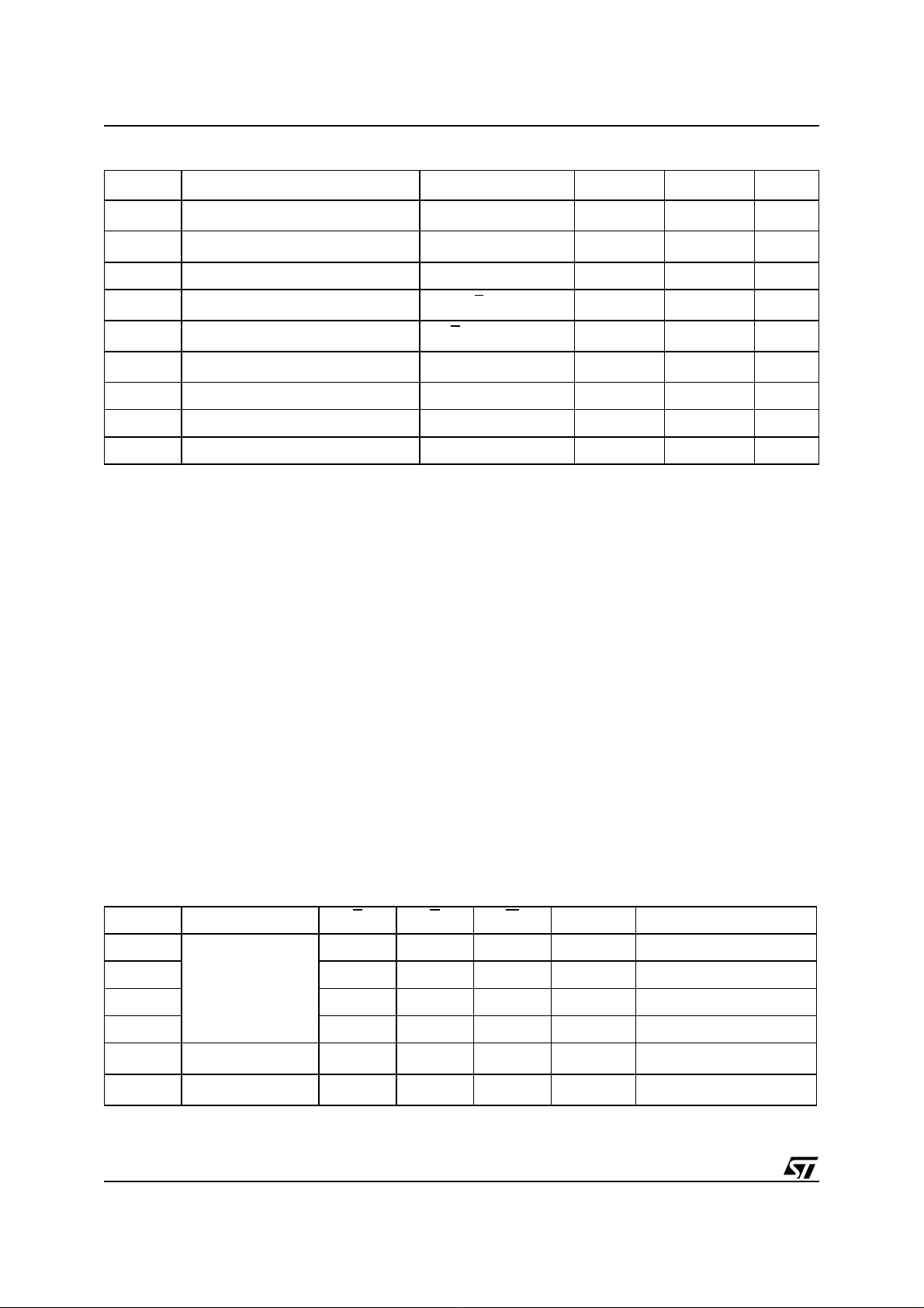
Table 11. Register Map
Address
D7 D6 D5 D4 D3 D2 D1 D0
7FF 10 Years Year Year 00-99
Data
Setting the Clock
The eighth bit of the cont rol register is t he WRITE
Bit. Setting the WRITE Bit to a '1,' like the READ
Bit, halts updates to the TI MEKEEPER registers.
The user can then load them wit h the correct day,
date, and time data in 24 hour BCD format (on Table11). Resetting the WRITE Bit to a '0' then transfers the values of all time registers (7F9-7FF) to
theactualTIMEKEEPER countersandallowsnormal operation to resume. The F T B it and the bits
marked as '0' in Table 11 must be written to '0' to
allow for normal TIMEKEEPER and RAM operation.
See the Application Note AN923, “TIMEKEEPER
Rolling Into the 21stCentury” for information on
Century Rollover.
Function/Range
BCD Format
®
7FE 0 0 0 10 M Month Month 01-12
7FD 0 0 10 Date Date Date 01-31
7FC 0 FT 0 0 0 Day Day 01-07
7FB 0 0 10 Hours Hours Hours 00-23
7FA 0 10 Minutes Minutes Minutes 00-59
7F9 ST 10 Seconds Seconds Seconds 00-59
7F8 W R S Calibration Control
Keys: S = SIGN Bit
FT = FREQUENCY TEST Bit (Set to '0' for normal clock operation)
R = READ Bit
W=WRITEBit
ST = STOP Bit
0=Mustbesetto'0'
12/19
Page 13

Stopping and Starting the Oscillator
The oscillator may be stopped at any time. If the
device is going to spend a significant amount of
time on the shelf, the oscillator can be turned off t o
minimize current drain on t he battery. The STOP
Bit is the MSB of the seconds register. Setting it to
a '1' stops the oscillator. The M48T02/12 is
shipped from STMicroelectronics with the STOP
Bit set to a '1.' When reset to a '0,' the M48T02/12
oscillator starts within one second.
Calibrating the Clock
The M48T02/12 is driven by a quartz-controlled
oscillator with a nomi nal f requency of 32,768 Hz.
A typica l M48T02/12 is accu rate within 1 minute
per month at 25°C without calibration. The devices
are tested not to exce ed ± 35 PPM (parts per million) oscillator frequency error at 25°C, which
equates to about ±1.53 minutes per month.
The oscillation rate of any crystal changes with
temperature. Figure 11, page 14 shows the frequency error that can be expected at vario us temperatures. Most clock chips compensate for
crystal frequency and temperature shift error with
cumbersome “trim” capacitors. The M48T02/12
design, howe ve r, employs periodic counter correction. The calibration circuit ad ds or subtracts
counts from the oscillator divider circuit at the divide by 256 stage, as shown in Figure 12, page 14.
The number of times pulses are blanke d (subtracted, negative c alibration) or split (added, positive
calibration) depends upon the value loaded into
the five-bit Calibration Byte found in the Control
Register. Addi ng counts speeds the clock up, subtracting counts slows the clock down.
The Calibration Byte occupies the five lower order
bits in the Control r egister. This byte can be set to
represent any value between 0 and 31 in binary
form. The sixth bit is the Sign Bit; '1' indicates positive calibration, '0' indicates negative calibration.
Calibration occurs within a 64 minute cycle. The
first 62 minutes in the cycle may, once per minute,
have one second either shortened by 128 or
lengthened by 256 oscillator cycles. If a binary '1'
is loaded into the register, only the first 2 minut es
in the 64 minute cycle will be modified; if a binary
6 is loaded, the first 12 will be affected, and so on.
Therefore, each calibration step has the effect of
adding 512 or subtracting 256 oscillator cycles for
every 125, 829,120 actual osc ill ator cycles; that is
+4.068 or –2.034 PPM of adjustment per calibra-
M48T02, M48T12
tion step in the c alibration register. Assuming that
theoscillator is in fact running at ex ac tly 32,768Hz,
each of the 31 increments in the Calibration Byte
would represent +10.7 or –5.35 seconds per
month which corresponds to a total ra nge of +5.5
or –2.75 minutes per month.
Two methods are available for ascertaining how
much calibration a given M48T02/12 may require.
The first involves simply setting the clock, letting it
run for a month and comparing it to a known accurate referenc e (like WWV broadc as t s ). While that
may s eem crude, it allows the designer to give the
end u se r the ability to calibrate his clock as his environment may require, even after the final product
is p ackaged in a non-user serviceable enclosure.
All the designer has to do is prov ide a simple utility
that accesses the Calibration Byte.
The second approach is better suited to a manufacturing environment, and in vo lves the use of
some test equipment. When the Frequency Test
(FT) Bit, the seventh-most significant bit in the Day
Register, is set to a '1,' and the oscillator is runn ing
at 32,768 Hz , the LSB (DQ0) of the Seconds Register will toggle at 512 Hz. Any deviation from 512
Hz indic ates the degree and direction of oscillator
frequency shift a t the test temperat ure. For example, a reading of 512.01024 Hz would indicate a
+20 PPM oscillator frequency error, requiring a –
10 (WR001010) to be loaded into the Calibration
Byte for correction.
Note: Setting or changing the C alibration Byte
does not affect the Frequenc y Test output frequency. The device must be selected and addresses mu st be stable at Address 7F9 when
reading the 512 Hz on DQ0.
The FT Bit must be set using the same method
used to set the clock: using the WRITE Bit. The
LSB of the Seconds Register is monitored by holding the M48T02/12 in an extended READ of the
Seconds Register, but without having the READ
Bit set . The FT Bit MUST be reset to '0' for normal
clock operations to res ume.
Note: It is not neces s ary to s et the WRI TE Bit
when setti ng or res etting the Frequency Test Bit
(FT) or the Stop Bit (ST).
For more inform ation on calibration, see the Application Note AN924, “TIMEKEEPER
®
Calibration.”
13/19
Page 14

M48T02, M48T12
Figure 11. Crystal Accuracy Across Temperature
ppm
20
0
-20
-40
-60
-80
-100
0 5 10 15 20 25 30 35 40 45 50 55 60 65 70
Figure 12. Clock Calibration
NORMAL
POSITIVE
CALIBRATION
NEGATIVE
CALIBRATION
∆F
= -0.038 (T - T
F
ppm
T0 = 25 °C
)2 ± 10%
0
2
C
°C
AI02124
AI00594B
14/19
Page 15

M48T02, M48T12
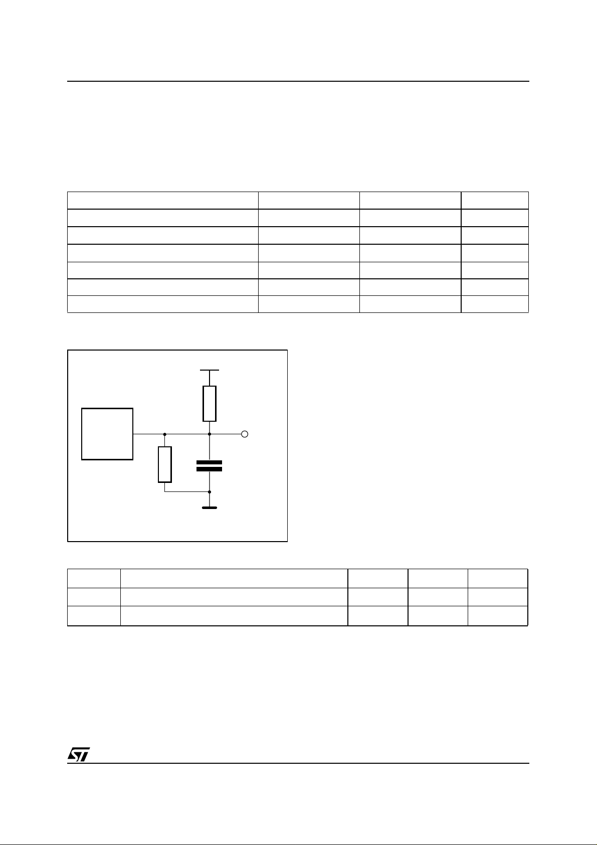
VCCNoise And Negative Going Transients
transients, including those produced by output
I
CC
switching, can produce voltage fluctuations, resultinginspikesontheV
bus. These transients
CC
can be reduced if capac itors are used to store energy wh ich stabilizes the V
bus. The energy
CC
stored in the bypass capacitors will be released as
low going spikes are generat ed or energy will be
absorbed when overshoots o ccur. A ceramic bypass capacitor value of 0.1µF (as shown in Figure
13) is recommended in order t o provide the needed filtering.
In addi tion to transients that are caused by normal
SRAM operation, power cycling can generate negative voltage spikes on V
below V
by as much as one volt. These negative
SS
that drive it to values
CC
spikes can cause data corruption in the SRAM
while in battery backup mode. To protect from
these voltage spikes, it is recommended to connect a schottky diode from V
connected to V
, anode to VSS). Schottky diode
CC
to VSS(cathode
CC
1N5817 is recommended for through ho le and
MBRS120T3 is recommended for surface mount.
Figure 13. Supply Voltage Protection
V
CC
V
CC
0.1µF DEVICE
V
SS
AI02169
15/19
Page 16

M48T02, M48T12
PART NUMBERING
Table 12. Ordering Information Scheme
Example: M48T 02 –70 PC 1 TR
Device Type
M48T
Supply Voltage and Write Protect Voltage
02 = V
12 = V
Speed
–70 = 100ns (M48T02/12)
–150 = 150ns (M48T02/12)
–200 = 200ns (M48T02/12)
= 4.75 to 5.5V; V
CC
= 4.5 to 5.5V; V
CC
= 4.5 to 4.75V
PFD
= 4.2 to 4.5V
PFD
Package
PC = PCDIP24
Temperature Range
1 = 0 to 70°C
Shipping Method for SOIC
blank = Tubes
TR = Tape & Reel
For a list of available options (e.g., Speed, Package) or for further information on any aspect of this device,
please contact the ST Sales Office nearest you.
16/19
Page 17

PACKAGE MECHANICAL INFORMATION
Figure 14. PCDIP24 – 24-pin Plastic DIP, battery CAPHAT, Package Outline
A2
M48T02, M48T12
A1AL
C
B1 B e1
eA
e3
D
N
E
1
Note: Drawing is not to scale.
PCDIP
Table 13. PCDIP24 – 24-pin Plastic DIP, battery C APHAT, Package Mechanica l Data
Symb
Typ Min Max Typ Min Max
A 8.89 9.65 0.350 0.380
A1 0.38 0.76 0.015 0.030
A2 8.38 8.89 0.330 0.350
B 0.38 0.53 0.015 0.021
mm inches
B1 1.14 1.78 0.045 0.070
C 0.20 0.31 0.008 0.012
D 34.29 34.80 1.350 1.370
E 17.83 18.34 0.702 0.722
e1 2.29 2.79 0.090 0.110
e3 25.15 30.73 0.990 1.210
eA 15.24 16.00 0.600 0.630
L 3.05 3.81 0.120 0.150
N24 24
17/19
Page 18

M48T02, M48T12
REVISION HISTORY
Table 14. Docum ent Revision History
Date Revision Details
July 2000 First issue
t
07/13/00
05/07/01 Reformatted; temp. / voltage info. added to tables (Tables 4, 5, 7, 8, 9, 10)
05/14/01 Note added to Clock Calibration section; table footnote correction (Table 6)
07/16/01 Basic formatting / content changes (Figure 1, Tables 4, 5, 10)
05/20/02 Add countries to disclaimer
change (Table 9)
REC
18/19
Page 19

M48T02, M48T12
Information furnished is believed to be accurate and reliable. However, STMicroelectronics assumes no responsibility for the consequences
of use ofsuch information nor forany infringement of patents or other rights of third parties which may result from its use. No license is granted
by implication or otherwise under any patent or patent rights of STMicroelectronics. Specifications mentioned in this publication are subject
to change without notice. This publication supersedes and replaces all information previously supplied. STMicroelectronics products are not
authorized for use as critical components in life support devices or systems without express written approval of STMicroelectronics.
The ST logo is registered trademark of STMicroelectronics
All other names are the property of their respective owners.
© 2002 STMicroelectronics - All Rights Reserved
Australia - Brazil - Canada - China - Finland - France - Germany - Hong Kong - India - Israel - Italy - Japan - Malaysia -
Malta - Morocco - Singapore - Spain - Sweden - Switzerland - United Kingdom - U.S.A.
STMicroelectronics GROUP OF COMPANIES
www.st.com
19/19
 Loading...