

STMicroelectronics LM148, LM248, LM348 User Manual
LM148
LM248
LM348
FOUR UA741
QUAD BIPOLAR OPERATIONAL AMPLIFIERS
■ LOW SUPPLY CURRENT: 0.53mA/AMPLI-
FIER
■ CLASS AB OUTPUT STAGE: NO CROSS
OVER DIST ORTION
■ PIN COMPATIBLE WITH LM124
■ LOW INPUT OFFSET VOLTAGE: 1mV
■ LOW INPUT OFFSET CURRENT: 2nA
■ LOW INPUT BIAS CURRENT : 30nA
■ GAIN BANDWIDTH PRODUCT: 1.3MHz
■ HIGH DEGREE OF IS OLATION BETWEEN
AMPLIFIERS: 120dB
■ OVERLOAD PROT ECTION FOR INPUTS
AND OUTPUTS
DESCRIPTION
The LM148 consists of four independent, high
gain internally compensated, low power operational amplifiers which have been designed to provide functional characteristics identical to those of
the familiar UA741 operat ional amplifier. In addition the total supply current for all four amplifiers is
compatible to the supply current of a single UA741
type op amp. Other features inclu de inpu t of fset
current and input bias current which are much less
than those of a standard UA741. Also, excellent
isolation between amplifiers has been achieved by
independently biasing each amplifier and using
layout techniques qhich minimize thermal coupling.
The LM148 can be used anywhere multiple
UA741 type amplifiers are being used and in applications where amplifier matching or high packaing
density is required.
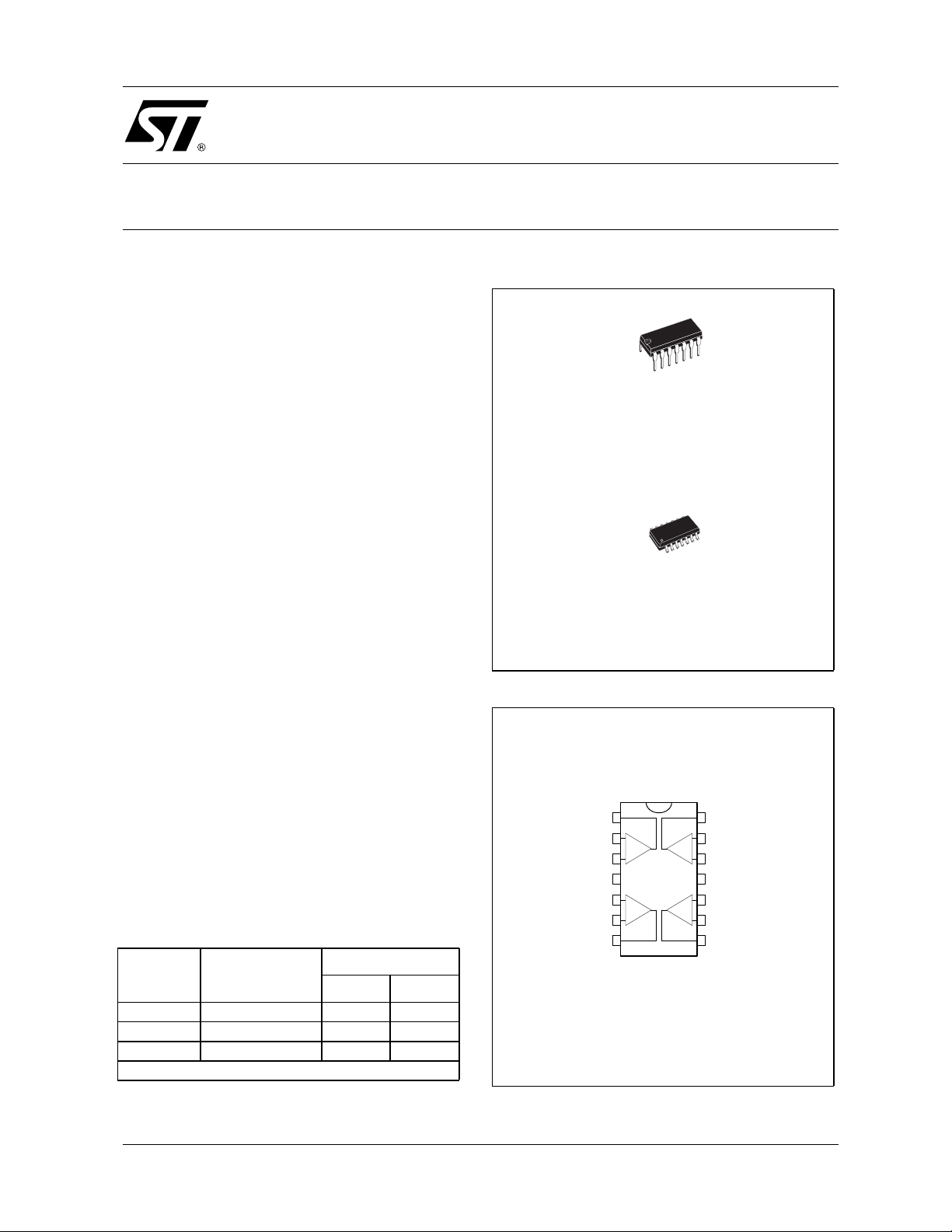
ORDER CODE
Part
Number
Temperature
Range
LM148 -55°C, +125°C
LM248 -40°C, +105°C
LM348 0°C, +70°C
Example : LM348D
Package
ND
••
••
••
N
DIP14
(Plastic Package)
D
(Plastic Micropackage)
PIN CONNECTIONS (top view)
1
Output 1
V
CC
Output 2
2
3
+
4
5
6
7
Inverting Input 1
Non-inverting Input 1
Non-inverting Input 2
Inverting Input 2
SO14
14
13
-
+
+
-
-
+
12
11
10
+
9
8
Output 4
Inverting Input 4
Non-inverting Input 4
-
V
CC
Non-inverting Input 3
Inverting Input 3
Output 3
N = Dual in Line Package (DIP)
D = Small Outline Package (SO) - also available i n Tape & Reel (DT)
March 2002
1/5
LM148-LM248-LM348
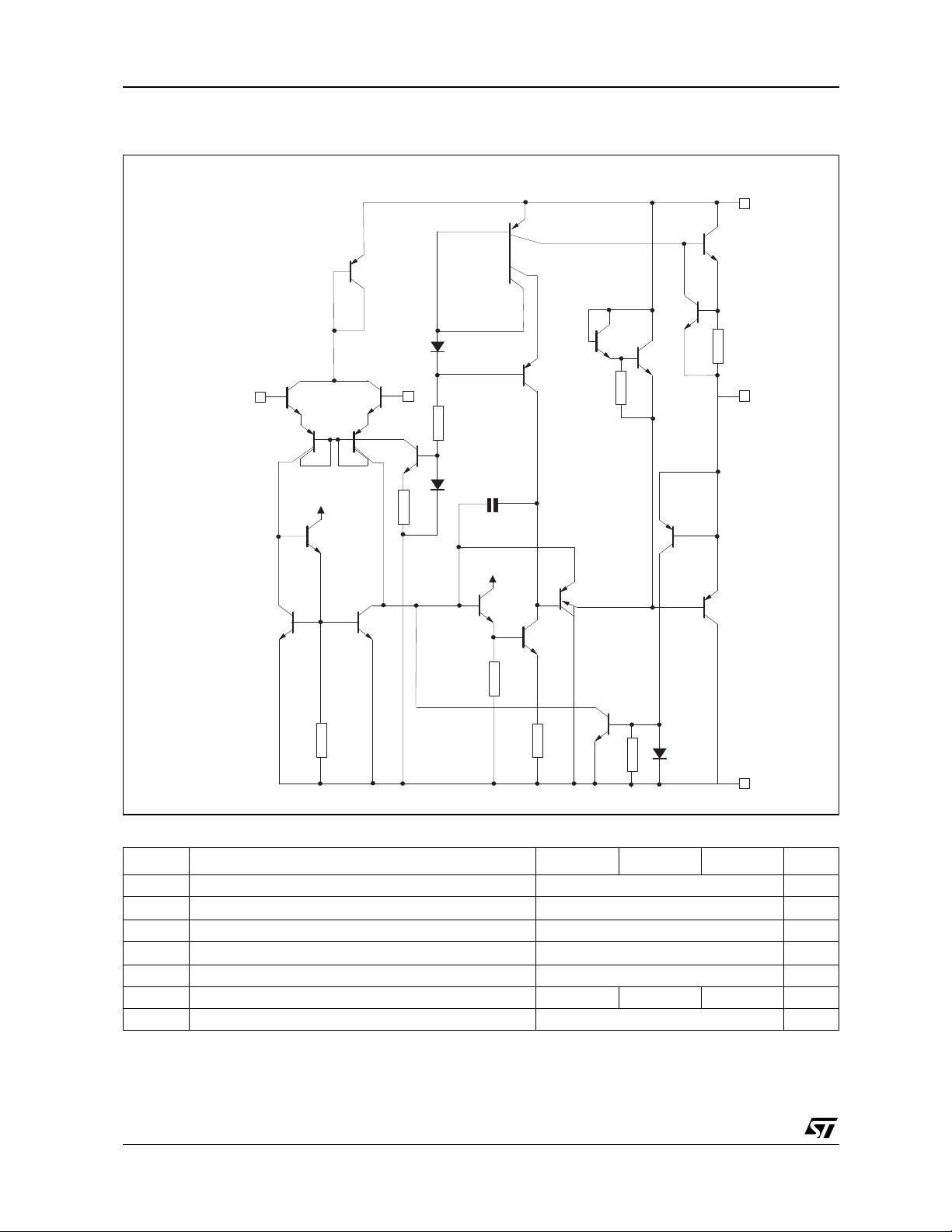
SCHEMATIC DIAGRAM
Non-inverting input
Inverting
input
Vcc+
25W
Output
350kW
Vcc+
2.5kW
60kW
7.4pF
Vcc+
60W
340W
36kW
Vcc-
ABSOLUTE MAXIMUM RATINGS
Symbol Parameter LM148 LM248 LM348 Unit
V
P
T
T
1. For supply voltage less than maximum value, the absolute maximum input voltage is equal to the supply voltage.
2. Any of the amplifier outputs can be shorted to ground indefinitly; however more than one should not be simultaneously shorted as the maximum
Supply voltage ±22 V
CC
V
Input Voltage
i
V
Differential Input Voltage ±44 V
id
Output Short-circuit Duration
Power Dissipation 500 mW
tot
Operating Free-air Temperature Range -55 to +125 -40 to +105 0 to +70 °C
oper
Storage Temperature Range -65 to +150 °C
stg
junction will be exceeded.
1)
2)
±22 V
Infinite
2/5
 Loading...