

STMicroelectronics LIS2L06AL Service Manual
www.DataSheet4U.com
LIS2L06AL
MEMS INERTIAL SENSOR:
2-axis - +/- 2g/6g ULTRACOMPACT LINEAR ACCELEROMETER
Features
■ 2.4V TO 5.25V SINGLE SUPPLY
OPERATION
■ LOW POWER CONSUMPTION
■ ±2g/±6g USER SELECTABLE FULL-SCALE
■ 0.3mg RESOLUTION OVER 100Hz
BANDWIDTH
■ EMBEDDED SELF TEST
■ OUTPUT VOLTAGE, OFFSET AND
SENSITIVITY RATIOMETRIC TO THE
SUPPLY VOLTAGE
■ HIGH SHOCK SURVIVABILITY
■ ECO-PACK COMPLIANT
Description
The LIS2L06AL is a low-power 2-axis linear
capacitive accelerometer that includes a sensing
element and an IC interface able to take the
information from the sensing element and to
provide an analog signal to the external world.
The sensing element, capable of detecting the
acceleration, is manufactured using a dedicated
process developed by ST to produce inertial
sensors and actuators in silicon.
The IC interface is manufactured using a standard
CMOS process that allows high level of integration
to design a dedicated circuit which is trimmed to
better match the sensing element characteristics.
The LIS2L06AL has a dynamically selectable full
scale of
±2g/±6g and it is capable of measuring
accelerations over a bandwidth of 2.0 kHz for all
axes. The device bandwidth may be reduced by
using external capacitances. A self-test capability
allows to check the mechanical and electrical
signal path of the sensor.
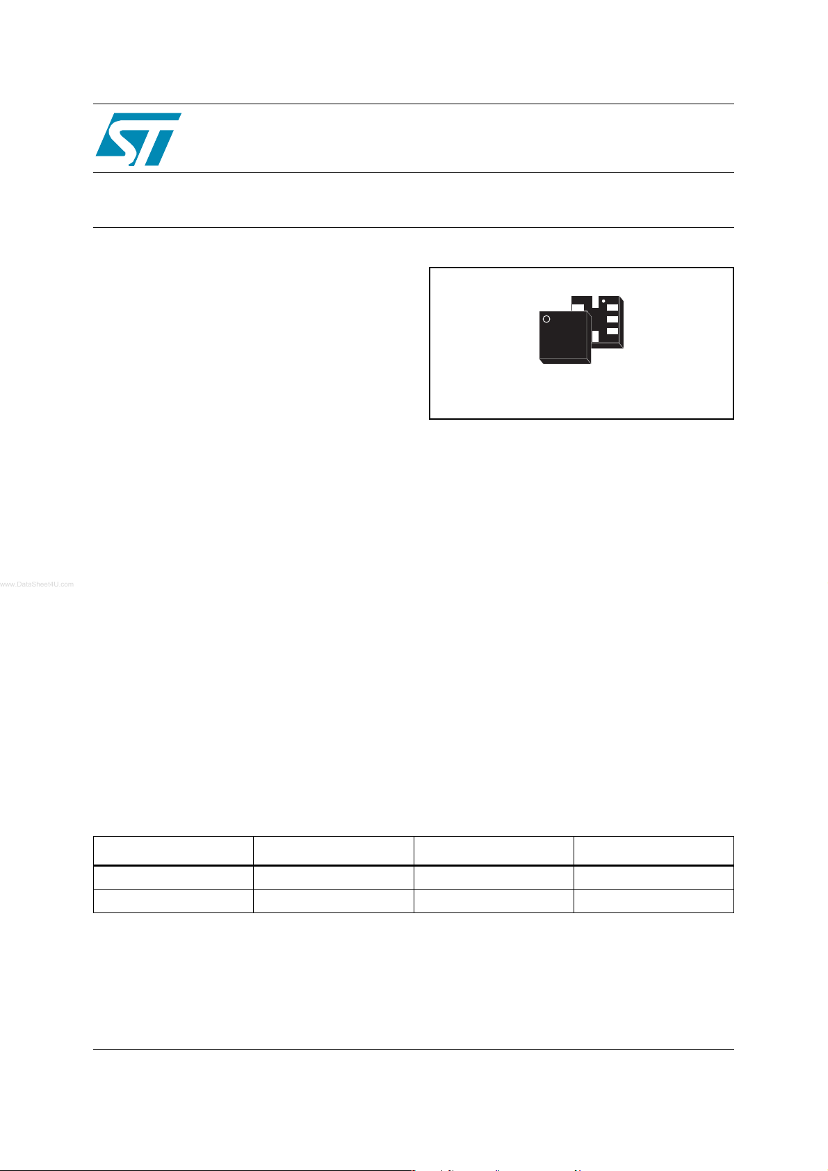
The LIS2L06AL is available in plastic SMD
package and it is guaranteed to operate over an
extended temperature range of -40°C to +85°C.
The LIS2L06AL belongs to a family of products
suitable for a variety of applications:
– Mobile terminals
– Gaming and Virtual Reality input devices
– Free-fall detection for data protection
– Antitheft systems and Inertial Navigation
– Appliance and Robotics.
LGA-8
Order codes
Part number Temp range, °C Package Packing
LIS2L06AL -40°C to +85°C LGA-8 Tray
LIS2L06ALTR -40°C to +85°C LGA-8 Tape & Reel
Rev 1
September 2005 CD00068417 1/17
www.st.com
17

LIS2L06AL
Contents
1 Block Diagram & Pins Description . . . . . . . . . . . . . . . . . . . . . . . . . . . . . . . 3
1.1 Block diagram . . . . . . . . . . . . . . . . . . . . . . . . . . . . . . . . . . . . . . . . . . . . . . . . . 3
1.2 Pin Description . . . . . . . . . . . . . . . . . . . . . . . . . . . . . . . . . . . . . . . . . . . . . . . . 3
2 Mechanical and Electrical Specifications . . . . . . . . . . . . . . . . . . . . . . . . . . 5
2.1 Mechanical Characteristics . . . . . . . . . . . . . . . . . . . . . . . . . . . . . . . . . . . . . . . 5
2.2 Electrical Characteristics . . . . . . . . . . . . . . . . . . . . . . . . . . . . . . . . . . . . . . . . 6
2.3 Absolute maximum ratings . . . . . . . . . . . . . . . . . . . . . . . . . . . . . . . . . . . . . . . 7
2.4 Terminology . . . . . . . . . . . . . . . . . . . . . . . . . . . . . . . . . . . . . . . . . . . . . . . . . . . 7
3 Functionality . . . . . . . . . . . . . . . . . . . . . . . . . . . . . . . . . . . . . . . . . . . . . . . . . 9
3.1 Sensing element . . . . . . . . . . . . . . . . . . . . . . . . . . . . . . . . . . . . . . . . . . . . . . . 9
3.2 IC Interface . . . . . . . . . . . . . . . . . . . . . . . . . . . . . . . . . . . . . . . . . . . . . . . . . . . 9
3.3 Factory calibration . . . . . . . . . . . . . . . . . . . . . . . . . . . . . . . . . . . . . . . . . . . . . . 9
4 Application hints . . . . . . . . . . . . . . . . . . . . . . . . . . . . . . . . . . . . . . . . . . . . . 10
4.1 Soldering information . . . . . . . . . . . . . . . . . . . . . . . . . . . . . . . . . . . . . . . . . . 11
4.2 Output Response vs Orientation . . . . . . . . . . . . . . . . . . . . . . . . . . . . . . . . . . 11
5 Typical performance characteristics . . . . . . . . . . . . . . . . . . . . . . . . . . . . . 12
5.1 Mechanical Characteristics at 25°C . . . . . . . . . . . . . . . . . . . . . . . . . . . . . . . 12
5.2 Mechanical Characteristics derived from measurement in the
-40°C to +85°C temperature range . . . . . . . . . . . . . . . . . . . . . . . . . . . . . . . . 13
5.3 Electrical characteristics at 25°C . . . . . . . . . . . . . . . . . . . . . . . . . . . . . . . . . 14
6 Package Information . . . . . . . . . . . . . . . . . . . . . . . . . . . . . . . . . . . . . . . . . . 15
7 Revision history . . . . . . . . . . . . . . . . . . . . . . . . . . . . . . . . . . . . . . . . . . . . . . 16
2/17 CD00068417
LIS2L06AL 1 Block Diagram & Pins Description
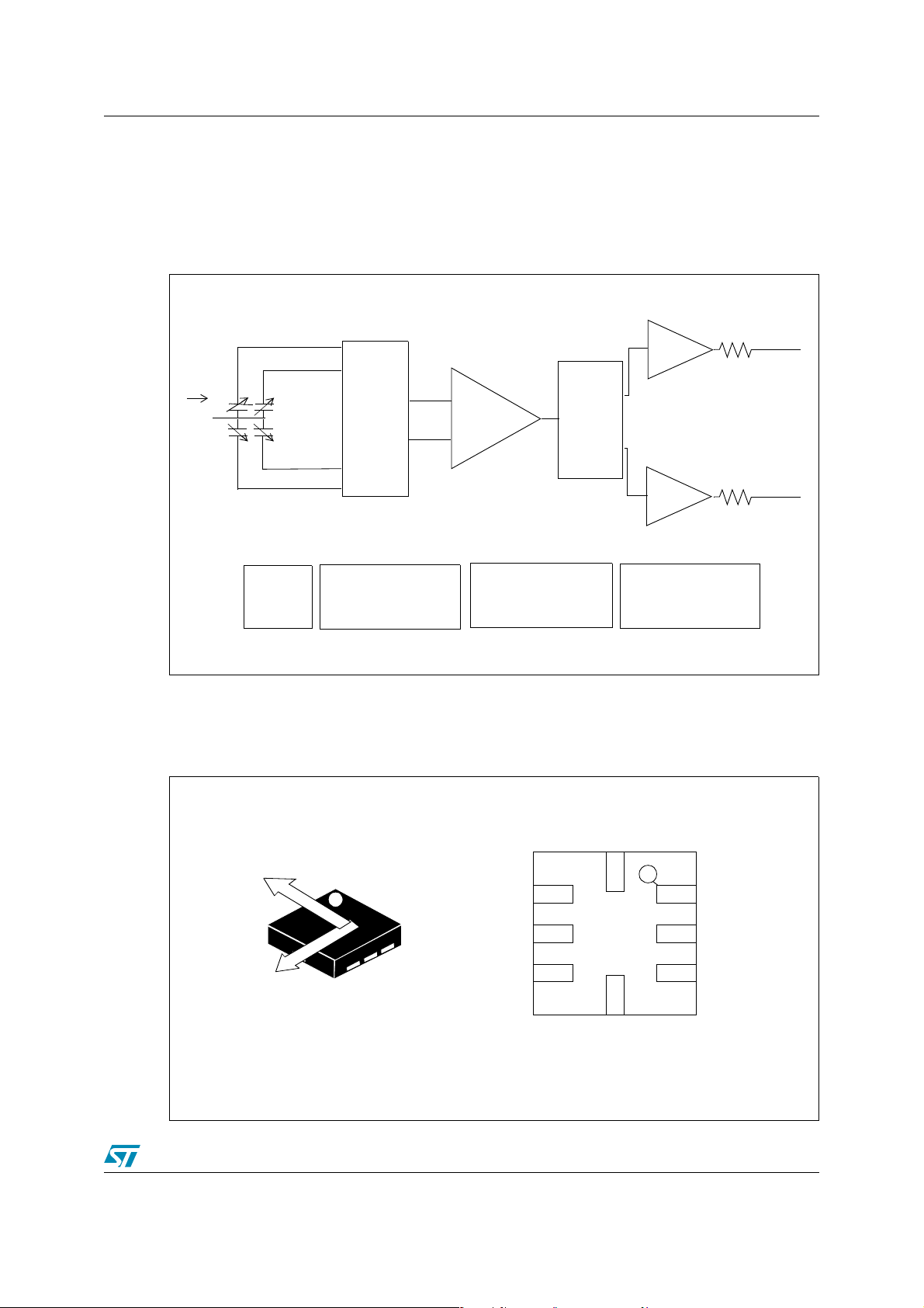
1 Block Diagram & Pins Description
1.1 Block diagram
Figure 1. Block Diagram
X+
Y+
a
Y-
X-
SELF TEST
1.2 Pin Description
Figure 2. Pin Connection
MUX
REFERENCE
CHARGE
AMPLIFIER
TRIMMING CIRCUIT
DEMUX
S/H
S/H
CLOCK
Routx
Routy
Voutx
Vouty
X
1
Y
DIRECTION OF THE
DETECTABLE
ACCELERATIONS
LIS2L06AL
Vdd
Voutx
Vouty
Reserved
Reserved
BOTTOM VIEW
CD00068417 3/17
ST
FS
GND
1 Block Diagram & Pins Description LIS2L06AL
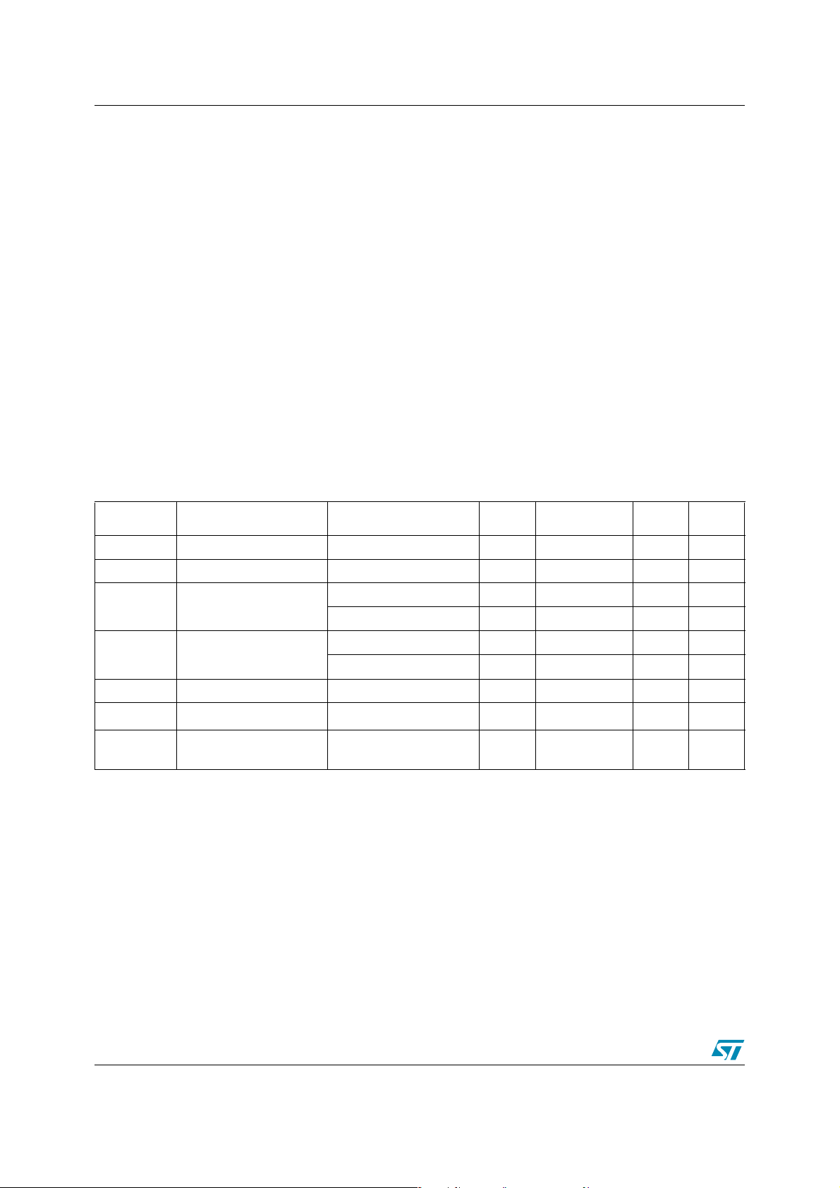
Table 1. Pin description
Pin # Pin Name Function
1 ST Self Test (Logic 0: normal mode; Logic 1: Self-test)
2FS
3 GND 0V supply
4 Reserved Leave unconnected
5 Reserved Leave unconnected
6 Vouty Output Voltage Y channel
7 Voutx Output Voltage X channel
8 Vdd Power supply
Full Scale(Logic 0:
2g Full scale; Logic 1: 6g Full Scale)
4/17 CD00068417
LIS2L06AL 2 Mechanical and Electrical Specifications
2 Mechanical and Electrical Specifications
2.1 Mechanical Characteristics
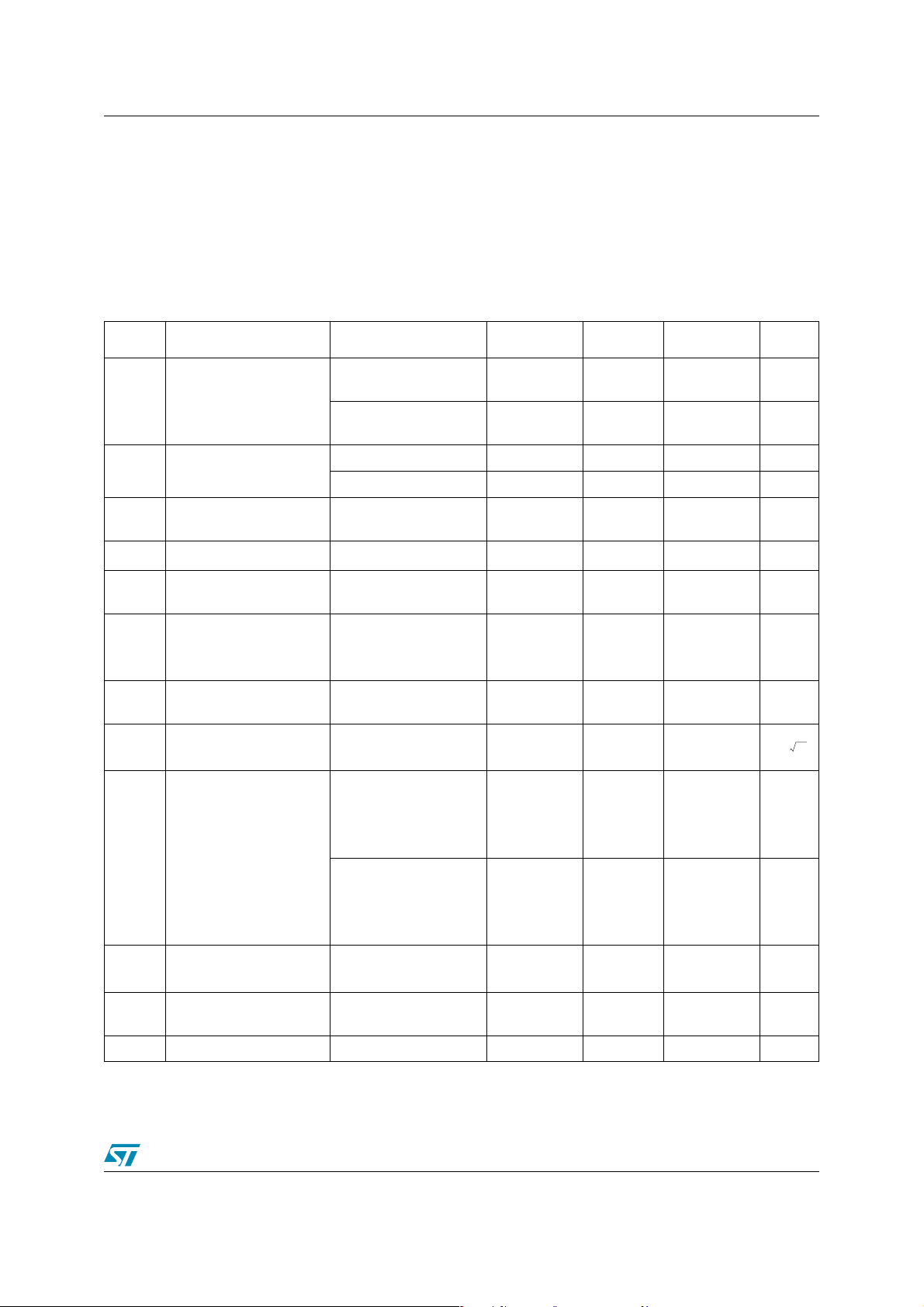
Table 2. Mechanical Characteristics1
(Temperature range -40°C to +85°C) All the parameters are specified @ Vdd =3.3V,
T = 25°C unless otherwise noted.
Symbol Parameter Test Condition Min.
Typ.
2
Max. Unit
Ar
So
SoDr
Voff
OffDr
NL
CrossA
x
An
Vt
Acceleration Range
Sensitivity
Sensitivity Change Vs
Temperature
Zero-g Level
Zero-g level Change Vs
Temperature
Non Linearity
Cross-Axis
Acceleration Noise
Density
Self test Output Voltage
Change
3
4
4
5
6
7,8,9
FS pin connected to
GND
FS pin connected to
Vdd
Full-scale = 2g Vdd/5–10% Vdd/5 Vdd/5+10% V/g
Full-scale = 6g Vdd/15–10% Vdd/15 Vdd/15+10% V/g
Delta from +25°C ±0.01 %/°C
T = 25°C Vdd/2-6% Vdd/2 Vdd/2+6% V
Delta from +25°C ±0.2 mg/°C
Best fit straight line
Full-scale = 2g
X, Y axis
Vdd=3.3V;
Full-scale = 2g
T = 25°C
Vdd=3.3V
Full-scale = 2g
X axis
T = 25°C
Vdd=3.3V
Full-scale = 2g
Y axis
±1.8 ±2.0 g
±5.4 ±6.0 g
±0.3 ±1.5 %FS
±2 ±4%FS
30
-20 -50 -100 mV
20 50 100 mV
µg/
Hz
Fres
To p
Wh Product Weight 0.08 gram
Sensing Element
Resonance Frequency
Operating Temperature
Range
10
all axes 2.0 kHz
-40 +85 °C
Note: 1 The product is factory calibrated at 3.3V. The device can be powered from 2.4V to 5.25V. Voff,
So and Vt parameters will vary with supply voltage.
CD00068417 5/17
2 Mechanical and Electrical Specifications LIS2L06AL
2 Typical specifications are not guaranteed.
3 Guaranteed by wafer level test and measurement of initial offset and sensitivity.
4 Zero-g level and sensitivity are essentially ratiometric to supply voltage.
5 Guaranteed by design.
6 Contribution to the measuring output of the inclination/acceleration along any perpendicular
axis.
7 Self test “output voltage change” is defined as Vout
(Vst=Logic1)
-Vout
(Vst=Logic0)
8 Self test “output voltage change” varies cubically with supply voltage.
9 When Full Scale is set to
±
2g range.
10 Minimum resonance frequency Fres=2.0kHz. Sensor bandwidth=1/(2*
±
6g, “self test output voltage change” is one third of the corresponding
π
*110kΩ*Cload) with
Cload>723pF.
2.2 Electrical Characteristics
Table 3. Electrical Characteristics
1
(Temperature range -40°C to +85°C) All the parameters are specified @ Vdd =3.3V, T=25°C
unless otherwise noted
Symbol Parameter Test Condition Min.
Vdd Supply Voltage 2.4 3.3 5.25 V
Idd Supply Current mean value 0.85 1.5 mA
Vst Self Test Input
Vfs Full Scale Input
Rout Output Impedance 80 110 140 kΩ
Cload
To p
Capacitive Load Drive
Operating Temperature
Range
Logic 0 level 0 0.3*Vdd V
Logic 1 level 0.7*Vdd Vdd V
Logic 0 level 0 0.3*Vdd V
Logic 1 level 0.7*Vdd Vdd V
3
723 pF
-40 +85 °C
Typ.
2
Max. Unit
Note: 1 The product is factory calibrated at 3.3V
2 Typical specifications are not guaranteed
3 Minimum resonance frequency Fres=2.0kHz. Sensor bandwidth=1/(2*
π
*110kΩ*Cload) with
Cload>723pF
6/17 CD00068417
 Loading...