

STMicroelectronics LF00 User Guide
VOLTAGE REGULATORS WITH INHIBIT
■ VERY LOW DROPOUT VOLTAGE (0.45V)
■ VERY LOW QUIESCENT CURRENT (TYP.
50 µA IN OFFMODE,500 µA IN ON MODE)
■ OUTPUT CURRENT UP TO 500 mA
■ LOGIC-CONTROLLED ELECTRONIC
SHUTDOWN
■ OUTPUT VOLTAGES OF 1.25; 1.5; 1.8; 2.5;
2.7; 3; 3.3; 3.5; 4; 4.5; 4.7; 5; 5.2; 5.5; 6; 8;
8.5; 9; 12V
■ INTERNAL CURRENT AND THERMAL LIMIT
■ ONLY 2 .2 µF FOR STABILITY
■ AVAILABLE IN ± 1% (AB) OR ± 2% (C)
SELECTION AT 25 °C
■ SUPPLY VOLTAGE REJECTION: 80db (TYP. )
■ TEMPERATURE RANGE: -40 TO 12 5 °C
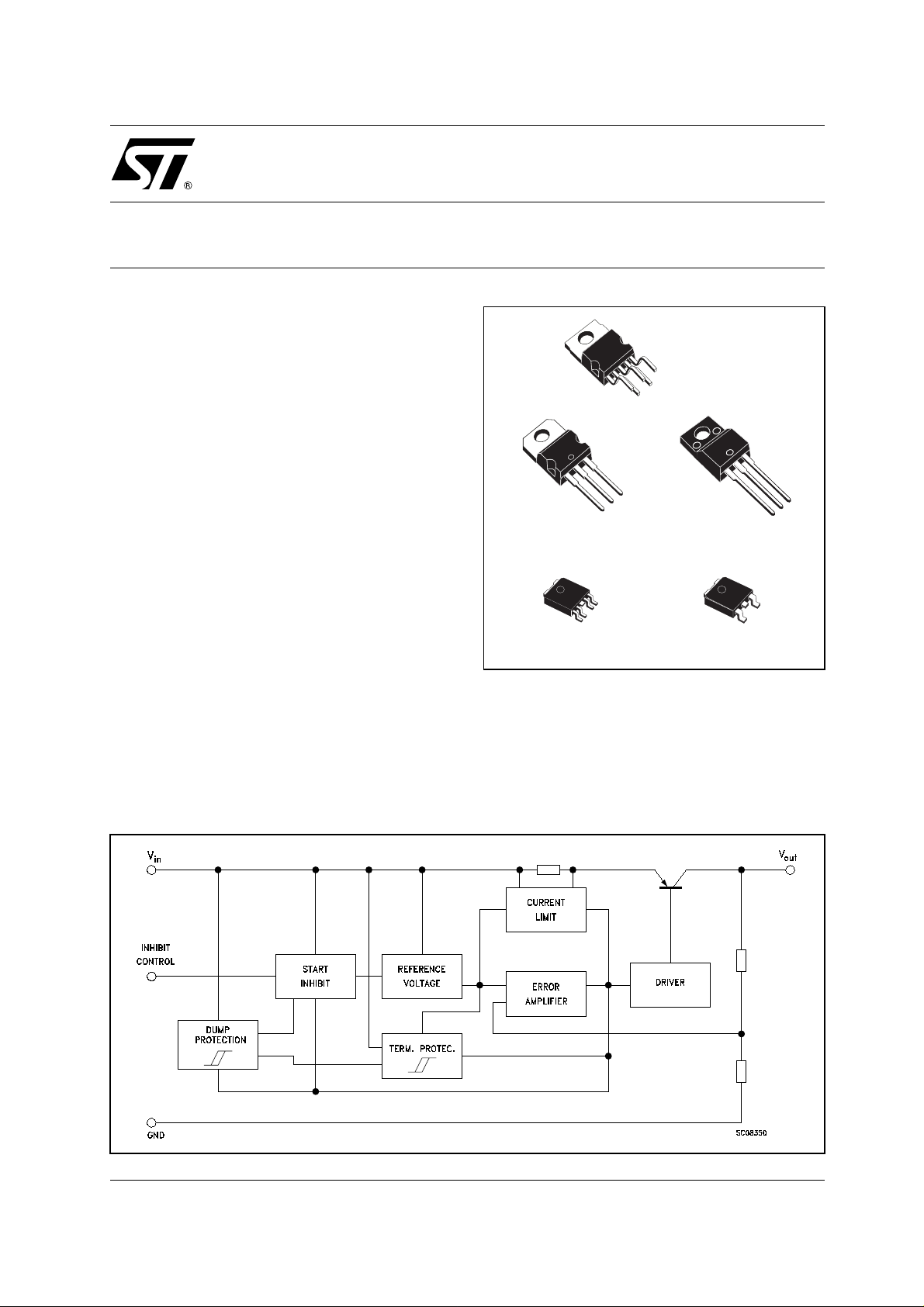
DESCRIPTION
The LF00 series are very Low Drop regulators
available in PENTAWA TT, TO-220, TO-220FP ,
DPAK and PPAK package and in a wide range of
output voltages.
The very Low Drop voltage (0.45V) and the very
low quiescent current make them particularly
suitable for Low Noise, Lo w Power applications
and specially in battery powered systems.
In the 5 pins configuration (PENTAW AT T and
PPAK) a Shutdown Logic Control function is
available (pin 2, TTL compatible). This means that
SCHEMATIC DIAGRAM
LF00
SERIES
VERY LOW DROP
PENTAWATT
TO-220
when the device is used as a local regulator, it is
possible to put a part of the board in standby,
decreasing the tot al power consumption. In t he
three terminal configuration the device has the
same electricalperformance, but is fixed in the ON
state. It requires only a 2.2 µF capacitor for
stability allowing space and cost saving.
TO-220FP
DPAKPPAK
1/34August 2003
LF00 SERIES
ABSOLUTE MAXIMUM RATINGS
Symbol Parameter Value Unit
V
I
P
T
T
(*) For 18 < VIN< 40 the regulator is in shut-down
THERMAL DATA
Symbol Parameter PENTAWATT TO-220 TO-220FP DPAK/PPAK Unit
R
thj-case
R
thj-amb
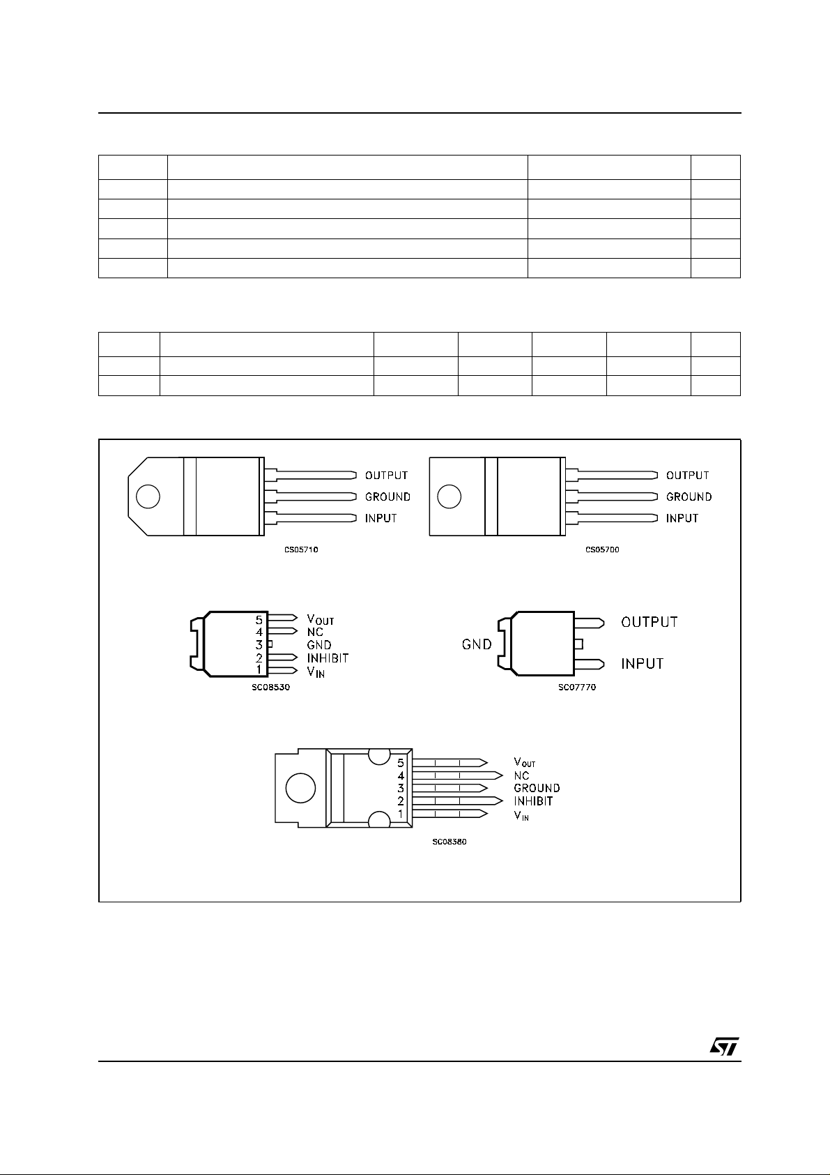
CONNECTION DIAGRAM (t op v iew)
DC Input Voltage
I
Output Current
O
Power Dissipation
tot
Storage Temperature Range
stg
Operating Junction Temperature Range
op
Thermal Resistance Junction-case
Thermal Resistance Junction-ambient
-0.5 to 40 (*) V
Internally Limited
Internally Limited
-40 to 150 °C
-40 to 125 °C
3358°C/W
50 50 60 100 °C/W
TO-220 TO-220FP
PPAK
DPAK
PENTAWATT
2/34
ORDERING CODES
LF00 SERIES
TYPE PENTAWATT TO-220 TO-220FP DPAK (#) PPAK (#)
LF12C (*) LF12CV5V LF12CV LF12CP LF12CDT LF12CPT 1.25 V
LF12AB (*) LF12ABV5V LF12ABV LF12ABP LF12ABDT LF12ABPT 1.25 V
LF15C LF15CV5V (*) LF15CV (*) LF15CP (*) LF15CDT LF15CPT (*) 1.5 V
LF15AB LF15ABV5V (*) LF15ABV (*) LF15ABP (*) LF15ABDT LF15ABPT (*) 1.5 V
LF18C LF18CV5V LF18CV LF18CP LF18CDT LF18CPT 1.8 V
LF18AB LF18ABV5V LF18ABV LF18ABP LF18ABDT LF18ABPT 1.8 V
LF25C LF25CV5V LF25CV LF25CP LF25CDT LF25CPT 2.5 V
LF25AB LF25ABV5V LF25ABV LF25ABP LF25ABDT LF25ABPT 2.5 V
LF27C LF27CV5V LF27CV LF27CP LF27CDT LF27CPT 2.7 V
LF27AB LF27ABV5V LF27ABV LF27ABP LF27ABDT LF27ABPT 2.7 V
LF30C LF30CV5V LF30CV LF30CP LF30CDT LF30CPT 3 V
LF30AB LF30ABV5V LF30ABV LF30ABP LF30ABDT LF30ABPT 3 V
LF33C LF33CV5V LF33CV LF33CP LF33CDT LF33CPT 3.3 V
LF33AB LF33ABV5V LF33ABV LF33ABP LF33ABDT LF33ABPT 3.3 V
LF35C LF35CV5V LF35CV LF35CP LF35CDT LF35CPT 3.5 V
LF35AB LF35ABV5V LF35ABV LF35ABP LF35ABDT LF35ABPT 3.5 V
LF40C LF40CV5V LF40CV LF40CP LF40CDT LF40CPT 4 V
LF40AB LF40ABV5V LF40ABV LF40ABP LF40ABDT LF40ABPT 4 V
LF45C (*) LF45CV5V LF45CV LF45CP LF45CDT LF45CPT 4.5 V
LF45AB (*) LF45ABV5V LF45ABV LF45ABP LF45ABDT LF45ABPT 4.5 V
LF47C LF47CV5V LF47CV LF47CP LF47CDT LF47CPT 4.75 V
LF47AB LF47ABV5V LF47ABV LF47ABP LF47ABDT LF47ABPT 4.75 V
LF50C LF50CV5V LF50CV LF50CP LF50CDT LF50CPT 5 V
LF50AB LF50ABV5V LF50ABV LF50ABP LF50ABDT LF50ABPT 5 V
LF52C LF52CV5V LF52CV LF52CP LF52CDT LF52CPT 5.2 V
LF52AB LF52ABV5V LF52ABV LF52ABP LF52ABDT LF52ABPT 5.2 V
LF55C LF55CV5V LF55CV LF55CP LF55CDT LF55CPT 5.5 V
LF55AB LF55ABV5V LF55ABV LF55ABP LF55ABDT LF55ABPT 5.5 V
LF60C LF60CV5V LF60CV LF60CP LF60CDT LF60CPT 6 V
LF60AB LF60ABV5V LF60ABV LF60ABP LF60ABDT LF60ABPT 6 V
LF80C LF80CV5V LF80CV LF80CP LF80CDT LF80CPT 8 V
LF80AB LF80ABV5V LF80ABV LF80ABP LF80ABDT LF80ABPT 8 V
LF85C LF85CV5V LF85CV LF85CP LF85CDT LF85CPT 8.5 V
LF85AB LF85ABV5V LF85ABV LF85ABP LF85ABDT LF85ABPT 8.5 V
LF90C LF90CV5V LF90CV LF90CP LF90CDT LF90CPT 9 V
LF90AB LF90ABV5V LF90ABV LF90ABP LF90ABDT LF90ABPT 9 V
LF120C LF120CV5V LF120CV LF120CP LF120CDT LF120CPT 12 V
LF120AB LF120ABV5V LF120ABV LF120ABP LF120ABDT LF120ABPT 12 V
(*) Available on request.
(#) Available in Tape & Reel with the suffix "-TR".
VOLTAGE
OUTPUT
3/34
LF00 SERIES
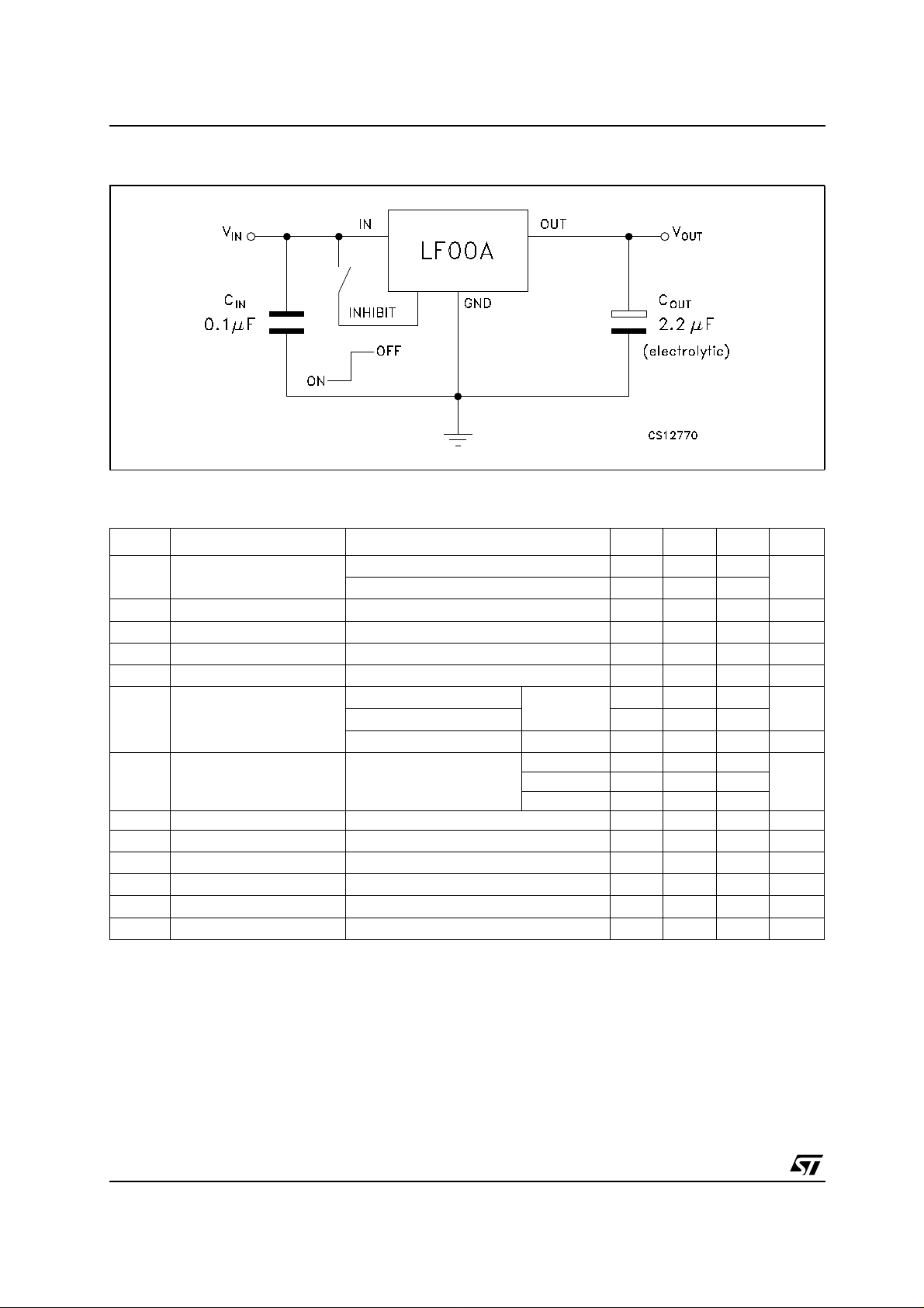
TEST CIRCUITS
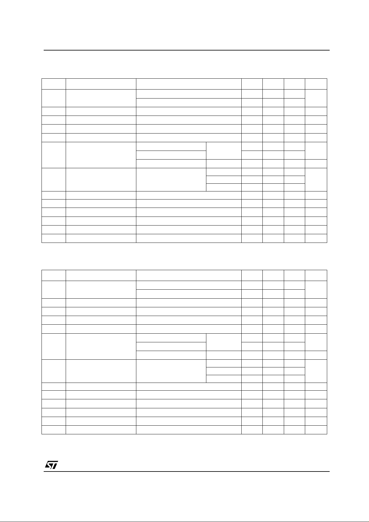
ELECTRICAL CHARACTERISTICS FOR LF12AB (refer to the test circuits, T
C
=2.2µF unless otherwise specified.)
O
=25°C,CI=0.1µF,
j
Symbol Parameter Test Conditions Min. Typ. Max. Unit
V
Output Voltage IO= 50 mA, VI= 3.3 V 1.238 1.25 1.263 V
O
= 50 mA, VI =3.3V,Ta= -25 to 85°C 1.225 1.275
I
O
V
Operating Input Voltage IO= 500 mA 2.5 16 V
I
Output Current Limit 1 A
I
O
∆V
∆V
SVR Supply Voltage Rejection I
Line Regulation VI = 2.5 to 16 V, IO= 5 mA 2 10 mV
O
Load Regulation VI = 2.8 V IO= 5 to 500 mA 2 10 mV
O
Quiescent Current VI = 2.5 to 16V, IO= 0mA ON MODE 0.5 1 mA
I
d
V
= 2.6 to 16V, IO= 500mA 12
I
= 6 V OFF MODE 50 100 µA
V
I
=5mA
O
V
= 3.5 ± 1 V
I
f = 120 Hz 82 dB
f=1KHz 77
f = 10 KHz 65
eN Output Noise Voltage B = 10 Hz to 100 KHz 50 µV
V
Dropout Voltage IO= 200 mA 1.25 V
d
Control Input Logic Low Ta= -40 to 125°C 0.8 V
V
IL
Control Input Logic High Ta= -40 to 125°C 2 V
V
IH
Control Input Current VI =6V, VC =6V 10 µA
I
I
Output Bypass Capacitance ESR = 0.1 to 10 Ω IO=0to500mA 2 10 µF
C
O
4/34
LF00 SERIES
ELECTRICAL CHARACTERISTICS FOR LF12C (refer to the test circuits, Tj=25°C,CI=0.1µF,
C
=2.2µF unless otherwise specified.)
O
Symbol Parameter Test Conditions Min. Typ. Max. Unit
V
Output Voltage IO= 50 mA, VI= 3.3 V 1.225 1.25 1.275 V
O
= 50 mA, VI = 3.3 V, Ta= -25 to 85°C 1.2 1.3
I
O
Operating Input Voltage IO= 500 mA 2.5 16 V
V
I
Output Current Limit 1 A
I
O
∆V
∆V
SVR Supply Voltage Rejection I
Line Regulation VI = 2.5 to 16 V, IO= 5 mA 2 10 mV
O
Load Regulation VI = 2.8 V IO= 5 to 500 mA 2 10 mV
O
Quiescent Current VI = 2.5 to 16V, IO= 0mA ON MODE 0.5 1 mA
I
d
= 2.6 to 16V, IO= 500mA 12
V
I
= 6 V OFF MODE 50 100 µA
V
I
=5mA
O
V
=3.5±1V
I
f = 120 Hz 82 dB
f = 1 KHz 77
f = 10 KHz 65
eN Output Noise Voltage B = 10 Hz to 100 KHz 50 µV
V
Dropout Voltage IO= 200 mA 1.25 V
d
Control Input Logic Low Ta= -40 to 125°C 0.8 V
V
IL
Control Input Logic High Ta= -40 to 125°C 2 V
V
IH
Control Input Current VI =6V, VC =6V 10 µA
I
I
Output Bypass Capacitance ESR = 0.1 to 10 Ω IO= 0 to 500 mA 2 10 µF
C
O
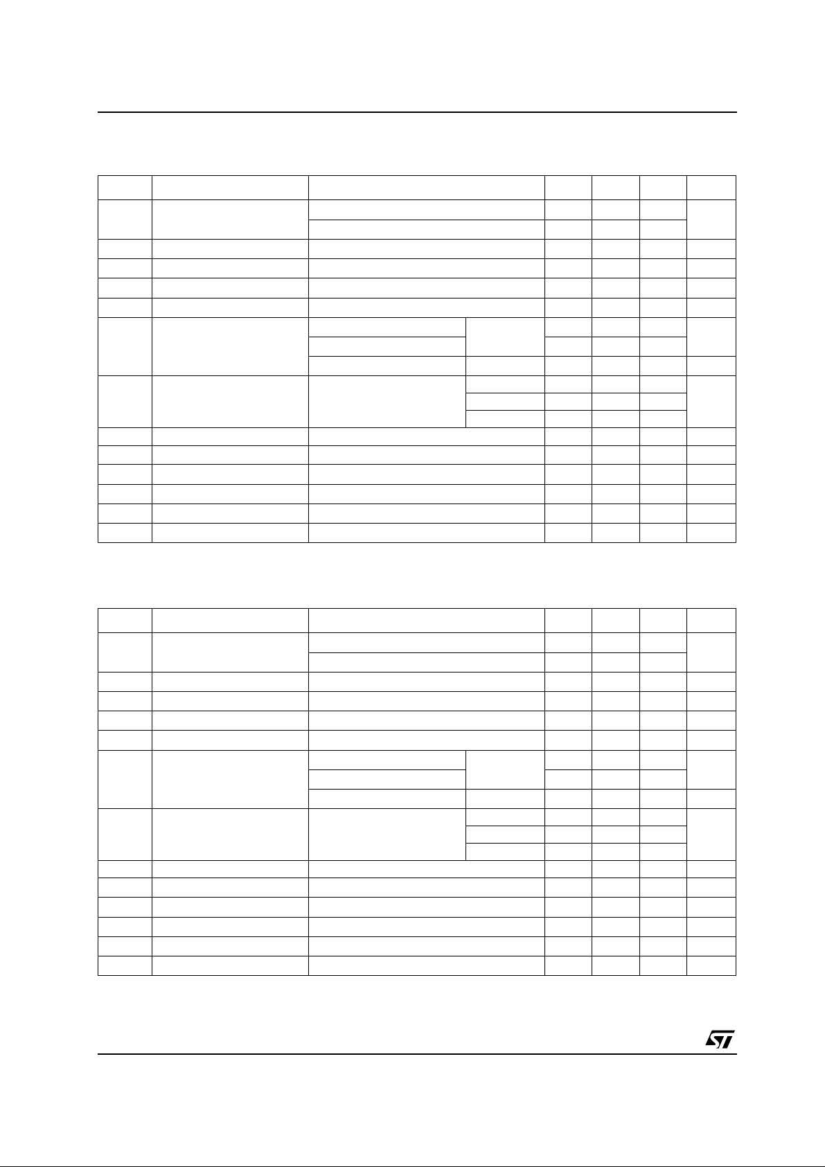
ELECTRICAL CHARACTERISTICS FOR LF15AB (refer to the test circuits, T
C
=2.2µF unless otherwise specified.)
O
=25°C,CI=0.1µF,
j
Symbol Parameter Test Conditions Min. Typ. Max. Unit
Output Voltage IO= 50 mA, VI= 3.5 V 1.485 1.5 1.515 V
V
O
= 50 mA, VI = 3.5 V, Ta= -25 to 85°C 1.470 1.530
I
O
Operating Input Voltage IO= 500 mA 2.5 16 V
V
I
Output Current Limit 1 A
I
O
∆V
∆V
SVR Supply Voltage Rejection I
Line Regulation VI = 2.5 to 16 V, IO= 5 mA 2 10 mV
O
Load Regulation VI = 2.8 V, IO= 5 to 500 mA 2 10 mV
O
Quiescent Current VI = 2.5 to 16V, IO= 0mA ON MODE 0.5 1 mA
I
d
= 2.8 to 16V, IO= 500mA 12
V
I
= 6 V OFF MODE 50 100 µA
V
I
=5mA
O
V
=3.5±1V
I
f = 120 Hz 82 dB
f = 1 KHz 77
f = 10 KHz 65
eN Output Noise Voltage B = 10 Hz to 100 KHz 50 µV
V
Dropout Voltage IO=200mA 1 V
d
Control Input Logic Low Ta= -40 to 125°C 0.8 V
V
IL
Control Input Logic High Ta= -40 to 125°C 2 V
V
IH
Control Input Current VI =6V, VC =6V 10 µA
I
I
Output Bypass Capacitance ESR = 0.1 to 10 Ω IO= 0 to 500 mA 2 10 µF
C
O
5/34
LF00 SERIES
ELECTRICAL CHARACTERISTICS FOR LF15C (refer to the test circuits, Tj= 25°C, CI=0.1µF,
C
=2.2µF unless otherwise specified.)
O
Symbol Parameter Test Conditions Min. Typ. Max. Unit
V
Output Voltage IO= 50 mA, VI= 3.5 V 1.47 1.5 1.53 V
O
= 50 mA, VI =3.5V,Ta= -25 to 85°C 1.44 1.56
I
O
Operating Input Voltage IO= 500 mA 2.5 16 V
V
I
Output Current Limit 1 A
I
O
∆V
∆V
SVR Supply Voltage Rejection I
Line Regulation VI = 2.5 to 16 V, IO= 5 mA 2 10 mV
O
Load Regulation VI = 2.8 V, IO= 5 to 500 mA 2 10 mV
O
Quiescent Current VI = 2.5 to 16V, IO= 0mA ON MODE 0.5 1 mA
I
d
= 2.8 to 16V, IO= 500mA 12
V
I
= 6 V OFF MODE 50 100 µA
V
I
=5mA
O
V
= 3.5 ± 1 V
I
f = 120 Hz 82 dB
f=1KHz 77
f = 10 KHz 65
eN Output Noise Voltage B = 10 Hz to 100 KHz 50 µV
V
Dropout Voltage IO= 200 mA 1 V
d
Control Input Logic Low Ta= -40 to 125°C 0.8 V
V
IL
Control Input Logic High Ta= -40 to 125°C 2 V
V
IH
Control Input Current VI =6V, VC =6V 10 µA
I
I
Output Bypass Capacitance ESR = 0.1 to 10 Ω IO=0to500mA 2 10 µF
C
O
ELECTRICAL CHARACTERISTICS FOR LF18AB (refer to the test circuits, T
C
=2.2µF unless otherwise specified.)
O
=25°C,CI=0.1µF,
j
Symbol Parameter Test Conditions Min. Typ. Max. Unit
Output Voltage IO= 50 mA, VI= 3.3 V 1.782 1.8 1.818 V
V
O
= 50 mA, VI =3.3V,Ta= -25 to 85°C 1.764 1.836
I
O
Operating Input Voltage IO= 500 mA 3 16 V
V
I
Output Current Limit 1 A
I
O
∆V
∆V
SVR Supply Voltage Rejection I
Line Regulation VI = 2.8 to 16 V, IO= 5 mA 2 12 mV
O
Load Regulation VI = 3.3 V, IO= 5 to 500 mA 2 10 mV
O
Quiescent Current VI = 2.5 to 16V, IO= 0mA ON MODE 0.5 1 mA
I
d
= 3.1 to 16V, IO= 500mA 12
V
I
= 6 V OFF MODE 50 100 µA
V
I
=5mA
O
V
= 3.5 ± 1 V
I
f = 120 Hz 82 dB
f=1KHz 77
f = 10 KHz 60
eN Output Noise Voltage B = 10 Hz to 100 KHz 50 µV
V
Dropout Voltage IO= 200 mA 0.7 V
d
V
Control Input Logic Low Ta= -40 to 125°C 0.8 V
IL
Control Input Logic High Ta= -40 to 125°C 2 V
V
IH
Control Input Current VI =6V, VC =6V 10 µA
I
I
Output Bypass Capacitance ESR = 0.1 to 10 Ω IO=0to500mA 2 10 µF
C
O
6/34
LF00 SERIES
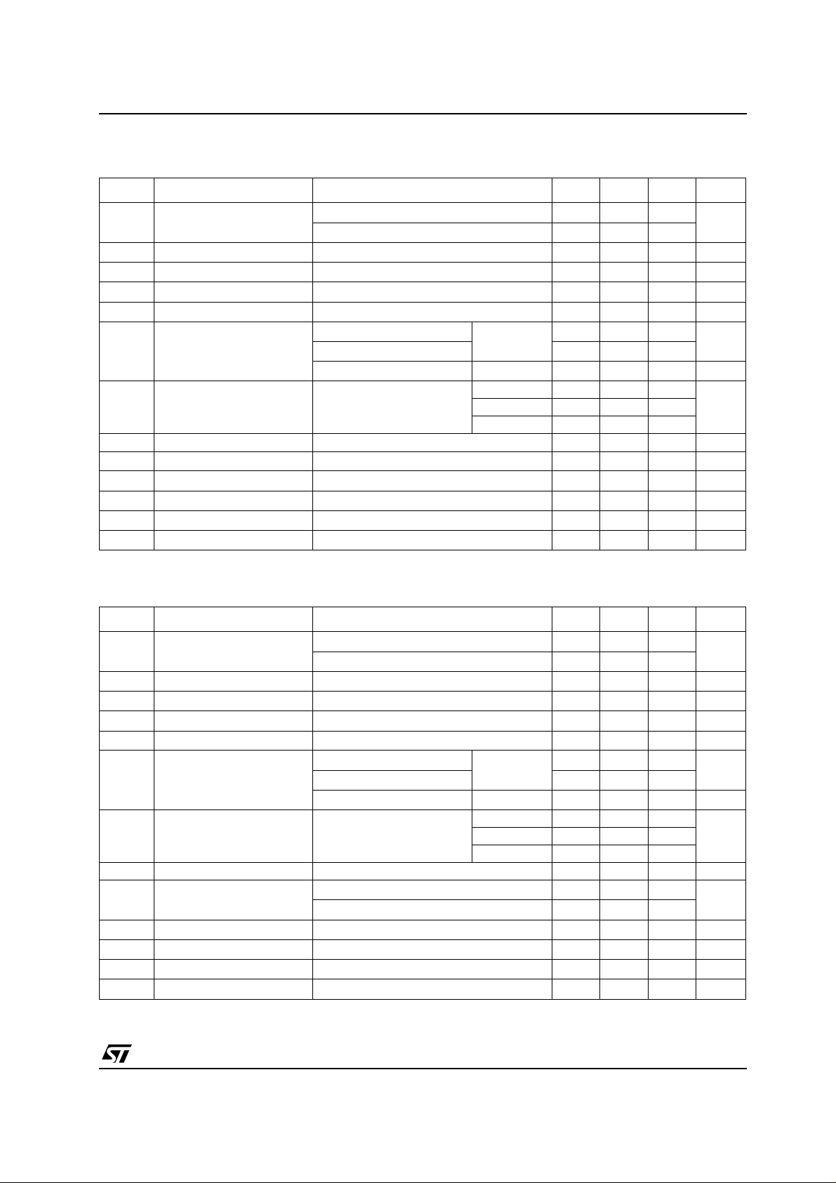
ELECTRICAL CHARACTERISTICS FOR LF18C (refer to the test circuits, Tj= 25°C, CI=0.1µF,
C
=2.2µF unless otherwise specified.)
O
Symbol Parameter Test Conditions Min. Typ. Max. Unit
V
Output Voltage IO= 50 mA, VI= 3.5 V 1.764 1.8 1.836 V
O
= 50 mA, VI =3.5V,Ta= -25 to 85°C 1.728 1.872
I
O
Operating Input Voltage IO= 500 mA 3 16 V
V
I
Output Current Limit 1 A
I
O
∆V
∆V
SVR Supply Voltage Rejection I
Line Regulation VI = 2.8 to 16 V, IO= 5 mA 2 12 mV
O
Load Regulation VI = 3.3 V, IO= 5 to 500 mA 2 10 mV
O
Quiescent Current VI = 2.5 to 16V, IO= 0mA ON MODE 0.5 1 mA
I
d
= 3.1 to 16V, IO= 500mA 12
V
I
= 6 V OFF MODE 50 100 µA
V
I
=5mA
O
V
= 3.5 ± 1 V
I
f = 120 Hz 82 dB
f=1KHz 77
f = 10 KHz 60
eN Output Noise Voltage B = 10 Hz to 100 KHz 50 µV
V
Dropout Voltage IO= 200 mA 0.7 V
d
Control Input Logic Low Ta= -40 to 125°C 0.8 V
V
IL
Control Input Logic High Ta= -40 to 125°C 2 V
V
IH
Control Input Current VI =6V, VC =6V 10 µA
I
I
Output Bypass Capacitance ESR = 0.1 to 10 Ω IO=0to500mA 2 10 µF
C
O
ELECTRICAL CHARACTERISTICS FOR LF25AB (refer to the test circuits, T
=2.2µF unless otherwise specified.)
C
O
=25°C,CI=0.1µF,
j
Symbol Parameter Test Conditions Min. Typ. Max. Unit
Output Voltage IO= 50 mA, VI= 4.5 V 2.475 2.5 2.525 V
V
O
= 50 mA, VI =4.5V,Ta= -25 to 85°C 2.450 2.550
I
O
Operating Input Voltage IO= 500 mA 16 V
V
I
Output Current Limit 1 A
I
O
∆V
∆V
SVR Supply Voltage Rejection I
Line Regulation VI = 3.5 to 16 V, IO= 5 mA 2 12 mV
O
Load Regulation VI = 3.8 V, IO= 5 to 500 mA 2 12 mV
O
Quiescent Current VI = 3.5 to 16V, IO= 0mA ON MODE 0.5 1 mA
I
d
= 3.8 to 16V, IO= 500mA 12
V
I
= 6 V OFF MODE 50 100 µA
V
I
=5mA
O
V
= 4.5 ± 1 V
I
f = 120 Hz 82 dB
f=1KHz 77
f = 10 KHz 65
eN Output Noise Voltage B = 10 Hz to 100 KHz 50 µV
V
Dropout Voltage IO= 200 mA 0.2 0.35 V
d
= 500 mA 0.4 0.7
I
O
Control Input Logic Low Ta= -40 to 125°C 0.8 V
V
IL
Control Input Logic High Ta= -40 to 125°C 2 V
V
IH
Control Input Current VI =6V, VC =6V 10 µA
I
I
Output Bypass Capacitance ESR = 0.1 to 10 Ω IO=0to500mA 2 10 µF
C
O
7/34

LF00 SERIES
ELECTRICAL CHARACTERISTICS FOR LF25C (refer to the test circuits, Tj= 25°C, CI=0.1µF,
C
=2.2µF unless otherwise specified.)
O
Symbol Parameter Test Conditions Min. Typ. Max. Unit
V
Output Voltage IO= 50 mA, VI= 4.5 V 2.45 2.5 2.55 V
O
= 50 mA, VI =4.5V,Ta= -25 to 85°C 2.4 2.6
I
O
Operating Input Voltage IO= 500 mA 16 V
V
I
Output Current Limit 1 A
I
O
∆V
∆V
SVR Supply Voltage Rejection I
Line Regulation VI = 3.5 to 16 V, IO= 5 mA 2 12 mV
O
Load Regulation VI = 3.8 V, IO= 5 to 500 mA 2 12 mV
O
Quiescent Current VI = 3.5 to 16V, IO= 0mA ON MODE 0.5 1 mA
I
d
= 3.8 to 16V, IO= 500mA 12
V
I
= 6 V OFF MODE 50 100 µA
V
I
=5mA
O
V
= 4.5 ± 1 V
I
f = 120 Hz 82 dB
f=1KHz 77
f = 10 KHz 65
eN Output Noise Voltage B = 10 Hz to 100 KHz 50 µV
V
Dropout Voltage IO= 200 mA 0.2 0.35 V
d
= 500 mA 0.4 0.7
I
O
Control Input Logic Low Ta= -40 to 125°C 0.8 V
V
IL
Control Input Logic High Ta= -40 to 125°C 2 V
V
IH
Control Input Current VI =6V, VC =6V 10 µA
I
I
Output Bypass Capacitance ESR = 0.1 to 10 Ω IO=0to500mA 2 10 µF
C
O
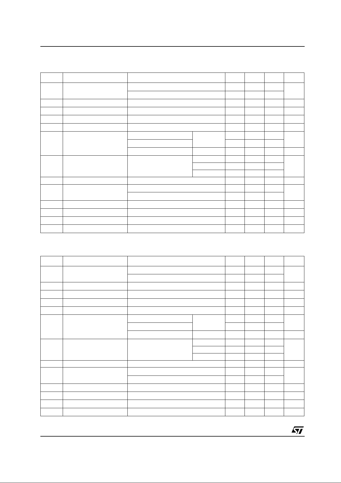
ELECTRICAL CHARACTERISTICS FOR LF27AB (refer to the test circuits, T
C
=2.2µF unless otherwise specified.)
O
=25°C,CI=0.1µF,
j
Symbol Parameter Test Conditions Min. Typ. Max. Unit
Output Voltage IO= 50 mA, VI= 4.7 V 2.673 2.7 2.727 V
V
O
= 50 mA, VI =4.7V,Ta= -25 to 85°C 2.646 2.754
I
O
Operating Input Voltage IO= 500 mA 16 V
V
I
Output Current Limit 1 A
I
O
∆V
∆V
SVR Supply Voltage Rejection I
Line Regulation VI = 3.7 to 16 V, IO= 5 mA 2 13 mV
O
Load Regulation VI =4V, IO= 5 to 500 mA 2 13 mV
O
Quiescent Current VI = 3.7 to 16V IO= 0mA ON MODE 0.5 1 mA
I
d
=4to16V IO= 500mA 12
V
I
= 6 V OFF MODE 50 100 µA
V
I
=5mA
O
V
= 4.7 ± 1 V
I
f = 120 Hz 82 dB
f=1KHz 77
f = 10 KHz 65
eN Output Noise Voltage B = 10 Hz to 100 KHz 50 µV
V
Dropout Voltage IO= 200 mA 0.2 0.35 V
d
= 500 mA 0.4 0.7
I
O
Control Input Logic Low Ta= -40 to 125°C 0.8 V
V
IL
V
Control Input Logic High Ta= -40 to 125°C 2 V
IH
Control Input Current VI =6V, VC =6V 10 µA
I
I
Output Bypass Capacitance ESR = 0.1 to 10 Ω IO=0to500mA 2 10 µF
C
O
8/34

LF00 SERIES
ELECTRICAL CHARACTERISTICS FOR LF27C (refer to the test circuits, Tj= 25°C, CI=0.1µF,
C
=2.2µF unless otherwise specified.)
O
Symbol Parameter Test Conditions Min. Typ. Max. Unit
V
Output Voltage IO= 50 mA, VI= 4.7 V 2.646 2.7 2.754 V
O
= 50 mA, VI =4.7V,Ta= -25 to 85°C 2.592 2.808
I
O
Operating Input Voltage IO= 500 mA 16 V
V
I
Output Current Limit 1 A
I
O
∆V
∆V
SVR Supply Voltage Rejection I
Line Regulation VI = 3.7 to 16 V IO= 5 mA 2 13 mV
O
Load Regulation VI =4V, IO= 5 to 500 mA 2 13 mV
O
Quiescent Current VI = 3.7 to 16V IO= 0mA ON MODE 0.5 1 mA
I
d
=4to16V IO= 500mA 12
V
I
= 6 V OFF MODE 50 100 µA
V
I
=5mA
O
V
= 4.7 ± 1 V
I
f = 120 Hz 82 dB
f=1KHz 77
f = 10 KHz 65
eN Output Noise Voltage B = 10 Hz to 100 KHz 50 µV
V
Dropout Voltage IO= 200 mA 0.2 0.35 V
d
= 500 mA 0.4 0.7
I
O
Control Input Logic Low Ta= -40 to 125°C 0.8 V
V
IL
Control Input Logic High Ta= -40 to 125°C 2 V
V
IH
Control Input Current VI =6V, VC =6V 10 µA
I
I
Output Bypass Capacitance ESR = 0.1 to 10 Ω IO=0to500mA 2 10 µF
C
O
ELECTRICAL CHARACTERISTICS FOR LF30AB (refer to the test circuits, T
C
=2.2µF unless otherwise specified.)
O
=25°C,CI=0.1µF,
j
Symbol Parameter Test Conditions Min. Typ. Max. Unit
Output Voltage IO= 50 mA, VI= 5 V 2.970 3 3.03 V
V
O
= 50 mA, VI =5V,Ta= -25 to 85°C 2.94 3.06
I
O
Operating Input Voltage IO= 500 mA 16 V
V
I
Output Current Limit 1 A
I
O
∆V
∆V
SVR Supply Voltage Rejection I
Line Regulation VI = 4 to 16 V, IO= 5 mA 3 15 mV
O
Load Regulation VI = 4.3 V, IO= 5 to 500 mA 3 15 mV
O
Quiescent Current VI = 4 to 16V, IO= 0mA ON MODE 0.5 1 mA
I
d
= 4.3 to 16V IO= 500mA 12
V
I
= 6 V OFF MODE 50 100 µA
V
I
=5mA
O
V
=5±1V
I
f = 120 Hz 81 dB
f=1KHz 76
f = 10 KHz 65
eN Output Noise Voltage B = 10 Hz to 100 KHz 50 µV
V
Dropout Voltage IO= 200 mA 0.2 0.35 V
d
= 500 mA 0.4 0.7
I
O
Control Input Logic Low Ta= -40 to 125°C 0.8 V
V
IL
V
Control Input Logic High Ta= -40 to 125°C 2 V
IH
Control Input Current VI =6V, VC =6V 10 µA
I
I
Output Bypass Capacitance ESR = 0.1 to 10 Ω IO=0to500mA 2 10 µF
C
O
9/34
LF00 SERIES
ELECTRICAL CHARACTERISTICS FOR LF30C (refer to the test circuits, Tj= 25°C, CI=0.1µF,
C
=2.2µF unless otherwise specified.)
O
Symbol Parameter Test Conditions Min. Typ. Max. Unit
V
Output Voltage IO= 50 mA, VI= 5 V 2.94 3 3.06 V
O
= 50 mA, VI =5V,Ta= -25 to 85°C 2.88 3.12
I
O
Operating Input Voltage IO= 500 mA 16 V
V
I
Output Current Limit 1 A
I
O
∆V
∆V
SVR Supply Voltage Rejection I
Line Regulation VI = 4 to 16 V, IO= 5 mA 3 15 mV
O
Load Regulation VI = 4.3 V, IO= 5 to 500 mA 3 15 mV
O
Quiescent Current VI = 4 to 16V, IO= 0mA ON MODE 0.5 1 mA
I
d
= 4.3 to 16V IO= 500mA 12
V
I
= 6 V OFF MODE 50 100 µA
V
I
=5mA
O
V
=5±1V
I
f = 120 Hz 81 dB
f=1KHz 76
f = 10 KHz 65
eN Output Noise Voltage B = 10 Hz to 100 KHz 50 µV
V
Dropout Voltage IO= 200 mA 0.2 0.35 V
d
= 500 mA 0.4 0.7
I
O
Control Input Logic Low Ta= -40 to 125°C 0.8 V
V
IL
Control Input Logic High Ta= -40 to 125°C 2 V
V
IH
Control Input Current VI =6V, VC =6V 10 µA
I
I
Output Bypass Capacitance ESR = 0.1 to 10 Ω IO=0to500mA 2 10 µF
C
O
ELECTRICAL CHARACTERISTICS FOR LF33AB (refer to the test circuits, T
C
=2.2µF unless otherwise specified.)
O
=25°C,CI=0.1µF,
j
Symbol Parameter Test Conditions Min. Typ. Max. Unit
Output Voltage IO= 50 mA, VI= 5.3 V 3.267 3.3 3.333 V
V
O
= 50 mA, VI =5.3V,Ta= -25 to 85°C 3.234 3.366
I
O
Operating Input Voltage IO= 500 mA 16 V
V
I
Output Current Limit 1 A
I
O
∆V
∆V
SVR Supply Voltage Rejection I
Line Regulation VI = 4.3 to 16 V, IO= 5 mA 3 16 mV
O
Load Regulation VI = 4.6 V, IO= 5 to 500 mA 3 16 mV
O
Quiescent Current VI = 4.3 to 16V, IO= 0mA ON MODE 0.5 1 mA
I
d
= 4.6 to 16V, IO= 500mA 12
V
I
V
= 6 V OFF MODE 50 100 µA
I
=5mA
O
V
= 5.3 ± 1 V
I
f = 120 Hz 80 dB
f=1KHz 75
f = 10 KHz 65
eN Output Noise Voltage B = 10 Hz to 100 KHz 50 µV
V
Dropout Voltage IO= 200 mA 0.2 0.35 V
d
= 500 mA 0.4 0.7
I
O
Control Input Logic Low Ta= -40 to 125°C 0.8 V
V
IL
Control Input Logic High Ta= -40 to 125°C 2 V
V
IH
Control Input Current VI =6V, VC =6V 10 µA
I
I
Output Bypass Capacitance ESR = 0.1 to 10 Ω IO=0to500mA 2 10 µF
C
O
10/34
LF00 SERIES
ELECTRICAL CHARACTERISTICS FOR LF33C (refer to the test circuits, Tj= 25°C, CI=0.1µF,
C
=2.2µF unless otherwise specified.)
O
Symbol Parameter Test Conditions Min. Typ. Max. Unit
V
Output Voltage IO= 50 mA, VI= 5.3 V 3.234 3.3 3.366 V
O
= 50 mA, VI =5.3V,Ta= -25 to 85°C 3.168 3.432
I
O
Operating Input Voltage IO= 500 mA 16 V
V
I
Output Current Limit 1 A
I
O
∆V
∆V
SVR Supply Voltage Rejection I
Line Regulation VI = 4.3 to 16 V, IO= 5 mA 3 16 mV
O
Load Regulation VI = 4.6 V, IO= 5 to 500 mA 3 16 mV
O
Quiescent Current VI = 4.3 to 16V, IO= 0mA ON MODE 0.5 1 mA
I
d
= 4.6 to 16V, IO= 500mA 12
V
I
= 6 V OFF MODE 50 100 µA
V
I
=5mA
O
V
= 5.3 ± 1 V
I
f = 120 Hz 80 dB
f=1KHz 75
f = 10 KHz 65
eN Output Noise Voltage B = 10 Hz to 100 KHz 50 µV
V
Dropout Voltage IO= 200 mA 0.2 0.35 V
d
= 500 mA 0.4 0.7
I
O
Control Input Logic Low Ta= -40 to 125°C 0.8 V
V
IL
Control Input Logic High Ta= -40 to 125°C 2 V
V
IH
Control Input Current VI =6V, VC =6V 10 µA
I
I
Output Bypass Capacitance ESR = 0.1 to 10 Ω IO=0to500mA 2 10 µF
C
O
ELECTRICAL CHARACTERISTICS FOR LF35AB (refer to the test circuits, T
C
=2.2µF unless otherwise specified.)
O
=25°C,CI=0.1µF,
j
Symbol Parameter Test Conditions Min. Typ. Max. Unit
Output Voltage IO= 50 mA, VI= 5.5 V 3.465 3.5 3.535 V
V
O
= 50 mA, VI =5.5V,Ta= -25 to 85°C 3.430 3.570
I
O
Operating Input Voltage IO= 500 mA 16 V
V
I
Output Current Limit 1 A
I
O
∆V
∆V
SVR Supply Voltage Rejection I
Line Regulation VI = 4.5 to 16 V, IO= 5 mA 3 17 mV
O
Load Regulation VI = 4.8 V, IO= 5 to 500 mA 3 17 mV
O
Quiescent Current VI = 4.5 to 16V, IO= 0mA ON MODE 0.5 1 mA
I
d
= 4.8 to 16V, IO= 500mA 12
V
I
= 6 V OFF MODE 50 100 µA
V
I
=5mA
O
V
= 5.5 ± 1 V
I
f = 120 Hz 79 dB
f=1KHz 74
f = 10 KHz 60
eN Output Noise Voltage B = 10 Hz to 100 KHz 50 µV
V
Dropout Voltage IO= 200 mA 0.2 0.35 V
d
= 500 mA 0.4 0.7
I
O
Control Input Logic Low Ta= -40 to 125°C 0.8 V
V
IL
V
Control Input Logic High Ta= -40 to 125°C 2 V
IH
Control Input Current VI =6V, VC =6V 10 µA
I
I
Output Bypass Capacitance ESR = 0.1 to 10 Ω IO=0to500mA 2 10 µF
C
O
11/34
 Loading...