STMicroelectronics L98SI User Manual

®
OCTAL SERIAL SOLENOID DRIVER
.
EIGHT LOW R
(0.5Ω AT I
.
8 BIT SERIAL INPUT DATA (SPI)
.
8 BIT SERIAL DIAGNOSTIC OUTPUT FOR
OVERLOAD AND OPEN CIRCUIT CONDITIONS
.
OUTPUT SHORT CIRCUIT PROTECTION
.
CHIP ENABLE SELECT FUNCTION (active low)
.
INTERNAL 36V CLAMPING FOR EACH OUTPUT
.
CASCADABLE WITH ANOTHER OCTAL
DRIVER
.
LOW QUIESCENT CURRENT (10mA MAX.)
.
PACKAGE PowerSO20
DESCRIPTION
The L98SI is an octal low s ide solen oid driver r ea
lized in Multipower-BCD technology particularly
suited for driving lamps, relays and solenoids in in-
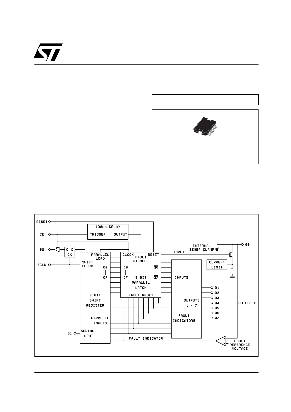
BLOCK DI A G RA M
= 1A @ 25°C VCC = 5V± 5%)
O
DMOS OUTPUTS
DSon
L98SI
MULTIPOWER BCD TECHNOLOGY
PowerSO2 0
ORDERING NUMBER:
dustrial environment. The L98SI DMOS outputs
have very low power co ns um ption.
Data is transmitted serially to the device using the
Serial Peripheral Interface (SPI) protocol.
The L98SI features the outputs status monitoring
function.
L98SI
Septembe r 20 03
1/9

L98SI
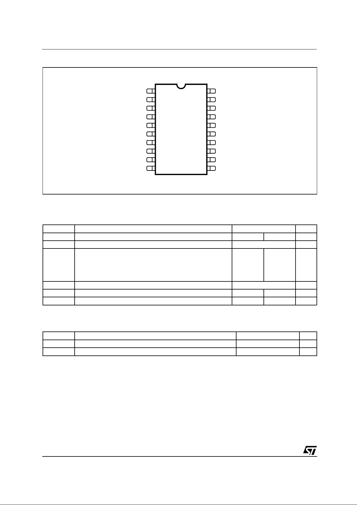
PIN CONNE CTION
(top view)
GND
SO
V
DD
RESET
OUT7
OUT6
OUT5
OUT4
N.C. N.C.
GND GND
2
3
4
5
6
7
8
9
10
D94AT119
20
19
18
17
16
15
14
13
12
11
GND1
SI
SCLK
CE
OUT0
OUT1
OUT2
OUT3
ABSOLUTE MAXIMUM RATINGS
Symbol Parameter Value Unit
V
DD
V
O
I
I
I
Odc
, T
T
j
E
X
DC Logic Supply – 0.7 7 V
Output Voltage internally clamped V
Input Transient Current
(CE, SI, SCLK, RESET, SO) :
Duration Time t = 1s,
V
V
< 0
I
> V
I
CC
– 25
Continuous Output Current (for each output) Int. Limited A
Junction and Storage Temperature Range – 40 150
stg
Max Clamping Energy (for each output) 200 mJ
+ 25
mA
mA
°
C
THERMAL DATA
Symbol Parameter Value Unit
Thermal Resistance Junction-Case Max. 1.5
Thermal Resistance Junction-Ambient Max. 60
2/9
R
th j- ca se
R
th j-amb
C/W
°
C/W
°

PIN DESCRIPTION
L98SI
V
CC
Logic supp ly vo lt age - no mi nally 5V
GROUND
Device Gr ound. This g round applies f or the logic circuits as we ll as t he po wer output stag es .
RESET
Asynchronou s reset for the ou t put stages, the par-
allel latc h and the shift register inside the L98SI. This
pin is active low and it must not be left floating. A
power on clear function may be implemented connecting this pin to V
with an external res istor and
CC
to ground w ith an ex t er na l ca pac it or .
CE
Chip Enable. Data is tran sfer r ed from the sh if t registers to t he output s on the r ising e dge of thi s signal.
The falling edge of this signal s et s the s hif t re gis t er
with the output voltage sense bits coming from the
output stages . The output driver for the SO pin is enabled whe n this pin is low.
SO
Serial Output. This pin is the serial output from the
shift register and it is tri-stated when CE is high. A
high for a da ta bit on this pin indicates th at th e pa r-
ticular out put is high. A low on this pin f o r a dat a bit
indicates th at th e output is low.
Comparing the serial output bits with the previous
serial input bits the external microcontroller implements the diag nos tic dat a s up plied by the L98S I .
SI
Serial Input . Th is pin i s the s er ial data inp ut. A hig h
on this pin will program a particular output to be OFF,
while a low wi ll tur n it ON.
SCLK
Serial Cl ock. This pin cl ocks the shift register. Ne w
SO data wil l appear on ev er y r is in g edge of th is pin
and new SI data will be latched on every SC LK’s falling edge into the s hif t re gis t er .
OUTPUTS 00- 07
Power output pins. The input and output bits corres-
ponding to 07 are sent and re ceived firs t via the SP I
bus and 00 is the las t. The outputs are provided w ith
current limi ting and voltage sense func tions for fa ult
indication and pr otec t io n. The nominal loa d c ur r ent
for these outputs is 500mA, but the current limiting
is set to a minimum o f 1.05A. T he outputs also h ave
on board clamps set at about 36V for recirculation
of inductive load current.
(V
ELECT RICAL CHARA CTE RISTICS
Symbol Parameter Test Conditions Min. Typ. Max. Unit
Output Clamping Volt. IO = 0.5A, Output Programmed OFF 30 40 V
Out. Leakage Current VO = 24V, Output Progr. OFF 1 mA
On Resistance Output Progr. ON
Out. Self Limiting
Current
Turn-on Delay IO = 500mA
Turn-off Delay IO = 500mA
Fault Refer. Voltage Output Progr. OFF
Fault Reset Delay
(after CE L to H
transition)
Out p u t O F F Vol t a g e Out put Pin Flo atin g.c Out put Pro gr. OFF , 1.0 V
I
R
V
V
V
OC
Oleak
DSon
I
OL
t
PHL
t
P
OREF
t
UD
OFF
= 5V ± 5%. Tj = – 40 to 125°C ; unless otherw is e s pec ii fed)
CC
I
= 0.5A
O
I
= 0.8A
O
I
= 1A
O
With Fault Reset Disabled
Output Progr. ON 1.05 A
No Reactive Load
No Reactive Load
1.6 2 V
Fault detected if V
See fig. 3 75 250
O
> V
OREF
0.55
0.55
0.55
1
1
1
10
10
Ω
Ω
Ω
s
µ
s
µ
s
µ
3/9
 Loading...