

STMicroelectronics L7800AB, L7800AC User Manual

■ OUTPUT CURRENT IN EXCESS OF 1A
■ OUTPUT VOLTAGES OF 5; 6; 8; 9; 12; 15;
18; 20; 24V
■ THERMAL OVERLOAD PROTECTION
■ OUTPUT TRANSITION SOA PROTECTION
■ 2% OUTPUT VOLTAGE TOLERANCE
■ GUARANTEED INEXTENDED
TEMPERATURE RANGE
DESCRIPTION
The L7800A series of three terminal positive
regulators is ava ilable in TO-220, TO-220FP,
TO-220FM and D
2
PAK packages and several
fixed output voltages, makin g it useful in a wide
range of applications. These regulators can
provide local on-card regu lation, eliminating the
distribution problem associated with si ngle point
regulation. Each type employs internal current
limiting, thermal shut-down and safe area
protection, making it ess enti ally i ndes tructible. If
adequate heat sinking is provided, they can
deliver over 1A output current, Although design ed
primarily as fixed voltage regulators, these
L7800AB/AC
SERIES
PRECISION 1A REGULATORS
TO-220
D2PAK
devices can be us ed with external components to
obtain adjustable voltage and currents.
TO-220FP
TO-220FM
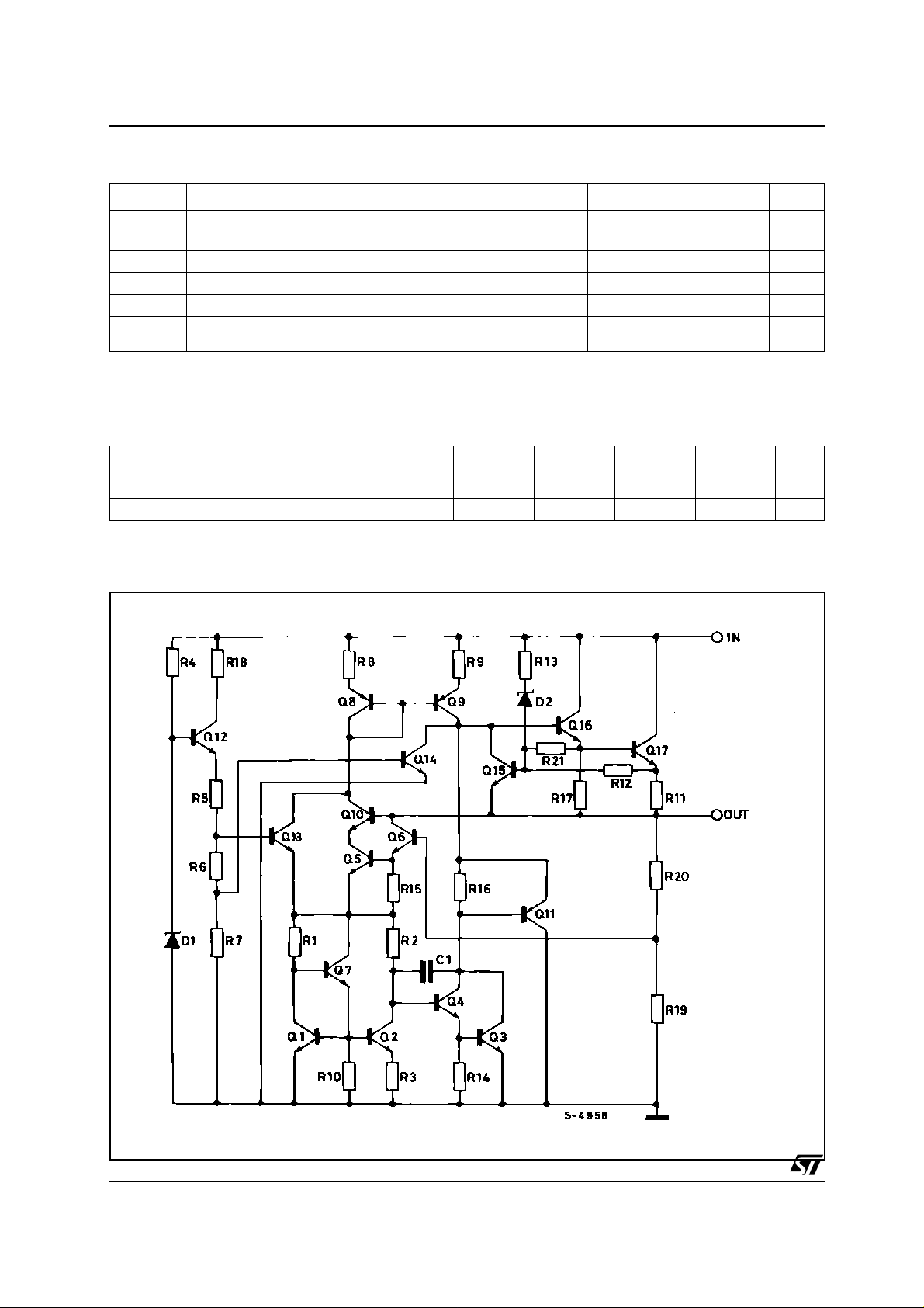
SCHEMATIC DIAGRAM
1/21March 2004
L7800AB/AC S ER IES
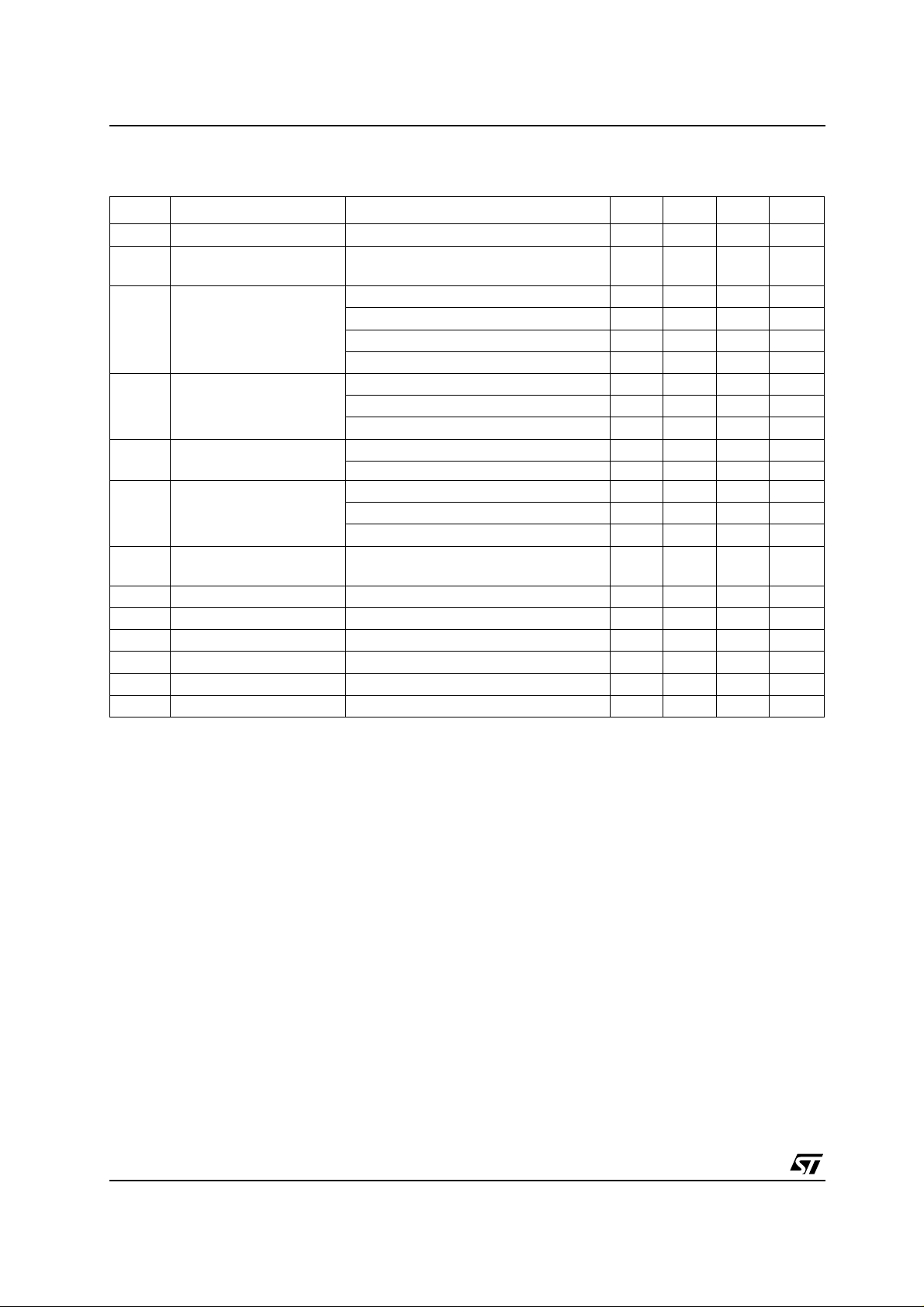
ABSOLUTE MAXIMUM RATINGS
Symbol Parameter Value Unit
V
I
P
T
T
Absolute Maximum Ratings are those values beyond which damage to the device may occur. Functional operation under these condition is
not implied.
DC Input Voltage (for VO=5to18V)
I
Output Current
O
Power Dissipation
D
Storage Temperature Range
stg
Operating Junction Temperature Range (for L7800AC)
op
(for V
= 20, 24V)
O
(for L7800AB)
THERMAL DATA
35
40
V
V
Internally Limited mA
Internally Limited mW
-65 to +150 °C
0to+150
-40 to +125
°C
°C
Symbol Parameter TO-220 TO-220FP TO-220FM
R
thj-case
R
thj-amb
Thermal Resistance Junction-case
Thermal Resistance Junction-ambient
3553°C/W
50 60 60 62.5 °C/W
SHEMATIC DIAGRAM
2
D
PAK
Unit
2/21
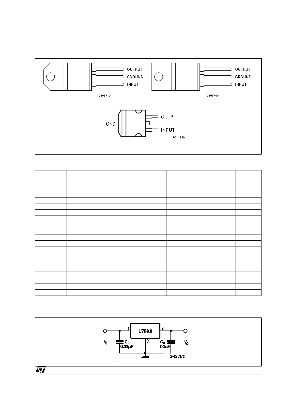
CONNECTION DIAGRAM (t op view)
L7800AB/AC SE RIES
TO-220 (Any Type)
TO-220FP/TO-220FM
D2PAK
ORDERING CODES
2
PAK
TYPE TO-220 TO-220FP TO-220FM
L7805AB L7805ABV L7805ABP L7805ABF L7805ABD2T 5 V
L7805AC L7805ACV L7805ACP L7805ACF L7805ACD2T L7805AC-D2TR 5 V
L7806AB L7806ABV L7806ABP L7806ABF L7806ABD2T 6 V
L7806AC L7806ACV L7806ACP L7806ACF L7806ACD2T 6 V
L7808AB L7808ABV L7808ABP L7808ABF L7808ABD2T 8 V
L7808AC L7808ACV L7808ACP L7808ACF L7808ACD2T 8 V
L7809AB L7809ABV L7809ABP L7809ABF L7809ABD2T 9 V
L7809AC L7809ACV L7809ACP L7809ACF L7809ACD2T 9 V
L7812AB L7812ABV L7812ABP L7812ABF L7812ABD2T 12 V
L7812AC L7812ACV L7812ACP L7812ACF L7812ACD2T 12 V
L7815AB L7815ABV L7815ABP L7815ABF L7815ABD2T 15 V
L7815AC L7815ACV L7815ACP L7815ACF L7815ACD2T 15 V
L7818AB L7818ABV L7818ABP L7818ABF L7818ABD2T 18 V
L7818AC L7818ACV L7818ACP L7818ACF L7818ACD2T 18 V
L7820AB L7820ABV L7820ABP L7820ABF L7820ABD2T 20 V
L7820AC L7820ACV L7820ACP L7820ACF L7820ACD2T 20 V
L7824AB L7824ABV L7824ABP L7824ABF L7824ABD2T 24 V
L7824AC L7824ACV L7824ACP L7824ACF L7824ACD2T 24 V
(*) Available in Tape & Reel with the suffix "-TR".
D
(A Type) (*)
D2PAK
(C Type) (T & R)
OUTPUT
VOLTAGE
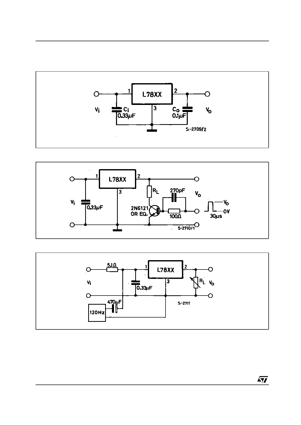
APPLICATION CIRCUITS
3/21
L7800AB/AC S ER IES
TEST CIRCUITS
Figure1 : DC Parameter
Figure2 : Load Regulation
Figure3 : Ripple Rejection
4/21
L7800AB/AC SE RIES
ELECTRICAL CHARACTERISTICS OF L7805A (VI=10V, IO=1A, TJ= 0 to 150°C (L7805AC),
= -40 to 125°C (L7805AB), unless otherwise specified.)
T
J
Symbol Parameter Test Conditions Min. Typ. Max. Unit
V
Output Voltage TJ= 25°C 4.9 5 5.1 V
O
V
Output Voltage IO=5mAto1A PO≤ 15W
O
(*) Line Regulation VI= 7.5 to 25V IO= 500 mA 7 50 mV
∆V
O
(*) Load Regulation IO= 5mA to 1A 25 100 mV
∆V
O
Quiescent Current TJ= 25°C 4.3 6 mA
I
q
∆I
Quiescent Current Change VI=8to25V IO= 500 mA 0.8 mA
q
SVR Supply Voltage Rejection V
V
Dropout Voltage IO=1A TJ= 25°C 2 V
d
eN Output Noise Voltage T
R
Output Resistance f =1KHz 17 mΩ
O
Short Circuit Current VI= 35V TA=25°C 0.2 A
I
sc
I
Short Circuit Peak Current TJ= 25°C 2.2 A
scp
/∆T Output Voltage Drift -1.1 mv/°C
∆V
O
V
= 7.5 to 20V
I
V
=8to12V 10 50 mV
I
=8to12V TJ= 25°C 2 25 mV
V
I
= 7.3 to 20V TJ= 25°C 7 50 mV
V
I
I
=5mAto1.5A TJ= 25°C 30 100 V
O
= 250 to 750mA 8 50 V
I
O
= 7.5 to 20V TJ= 25°C 0.8 mA
V
I
I
=5mAto1A 0.5 mA
O
= 8 to 18V f = 120Hz
I
I
= 500mA
O
= 25°C B =10Hz to 100KHz 10 µV/V
A
4.8 5 5.2 V
6mA
68 dB
O
(*) Load and Line Regulation are specified atconstant junction temperature. Changes in VOdue to heating effects must be taken into account
separately. Pulse testing with low dutycycle is used.
5/21
L7800AB/AC S ER IES
ELECTRICAL CHARACTERISTICS OF L7806A (VI=11V, IO=1A, TJ= 0 to 150°C (L7806AC),
= -40 to 125°C (L7806AB), unless otherwise specified.)
T
J
Symbol Parameter Test Conditions Min. Typ. Max. Unit
V
Output Voltage TJ= 25°C 5.88 6 6.12 V
O
V
Output Voltage IO=5mAto1A PO≤ 15W
O
(*) Line Regulation VI= 8.6 to 25V IO= 500 mA 9 60 mV
∆V
O
(*) Load Regulation IO= 5mA to 1A 25 100 mV
∆V
O
Quiescent Current TJ= 25°C 4.3 6 mA
I
q
∆I
Quiescent Current Change VI=9to25V IO= 500 mA 0.8 mA
q
SVR Supply Voltage Rejection V
Dropout Voltage IO=1A TJ= 25°C 2 V
V
d
eN Output Noise Voltage T
R
Output Resistance f =1KHz 17 mΩ
O
I
Short Circuit Current VI= 35V TA=25°C 0.2 A
sc
Short Circuit Peak Current TJ= 25°C 2.2 A
I
scp
/∆T Output Voltage Drift -0.8 mV/°C
∆V
O
(*) Load and Line Regulation are specified atconstant junction temperature. Changes in VOdue to heating effects must be taken into account
separately. Pulse testing with low dutycycle is used.
V
= 8.6 to 21V
I
V
=9to13V 11 60 mV
I
=9to13V TJ= 25°C 3 30 mV
V
I
= 8.3 to 21V TJ= 25°C 9 60 mV
V
I
I
=5mAto1.5A TJ= 25°C 30 100 V
O
= 250 to 750mA 10 50 V
I
O
= 8.6 to 21V TJ= 25°C 0.8 mA
V
I
I
=5mAto1A 0.5 mA
O
= 9 to 19V f = 120Hz
I
I
= 500mA
O
= 25°C B =10Hz to 100KHz 10 µV/V
A
5.76 6 6.24 V
6mA
65 dB
O
6/21

L7800AB/AC SE RIES
ELECTRICAL CHARACTERISTICS OF L7808A (VI=14V, IO=1A, TJ= 0 to 150°C (L7808AC),
= -40 to 125°C (L7808AB), unless otherwise specified.)
T
J
Symbol Parameter Test Conditions Min. Typ. Max. Unit
V
Output Voltage TJ= 25°C 7.84 8 8.16 V
O
V
Output Voltage IO=5mAto1A PO≤ 15W
O
(*) Line Regulation VI= 10.6 to 25V IO= 500 mA 12 80 mV
∆V
O
(*) Load Regulation IO= 5mA to 1A 25 100 mV
∆V
O
Quiescent Current TJ= 25°C 4.3 6 mA
I
q
∆I
Quiescent Current Change VI=11to25V IO= 500 mA 0.8 mA
q
SVR Supply Voltage Rejection V
Dropout Voltage IO=1A TJ= 25°C 2 V
V
d
eN Output Noise Voltage T
R
Output Resistance f =1KHz 18 mΩ
O
I
Short Circuit Current VI= 35V TA=25°C 0.2 A
sc
Short Circuit Peak Current TJ= 25°C 2.2 A
I
scp
/∆T Output Voltage Drift -0.8 mV/°C
∆V
O
(*) Load and Line Regulation are specified atconstant junction temperature. Changes in VOdue to heating effects must be taken into account
separately. Pulse testing with low dutycycle is used.
V
=10.6 to 23V
I
V
= 11 to 17V 15 80 mV
I
=11to17V TJ= 25°C 5 40 mV
V
I
= 10.4 to 23V TJ= 25°C 12 80 mV
V
I
I
=5mAto1.5A TJ= 25°C 30 100 V
O
= 250 to 750mA 10 50 V
I
O
= 10.6 to 23V TJ= 25°C 0.8 mA
V
I
I
=5mAto1A 0.5 mA
O
= 11.5 to 21.5V f = 120Hz
I
I
= 500mA
O
= 25°C B =10Hz to 100KHz 10 µV/V
A
7.7 8 8.3 V
6mA
62 dB
O
7/21
 Loading...