

Page 1
L6562
Fi
TRANSITION-MODE PFC CONTROLLER
1 FEATURES
■ REALISED IN BCD TECHNOLOGY
■ TRANSITION-MODE CONTROL OF PFC PRE-
REGULATORS
■ PROPRIETARY MULTIPLIER DESIGN F OR
MINIMUM THD OF AC INPUT CURRENT
■ VERY PRECISE ADJUSTABLE OUTPUT
OVERVOLTAGE PROTECTION
■ ULTRA-LOW (≤70µA) START-UP CURRENT
■ LOW (≤4 mA) QUIESCENT CURRENT
■ EXTENDED IC SUPPLY VOLTAGE RANGE
■ ON-CHIP FILTER ON CURRENT SENSE
■ DISABLE FUNCTION
■ 1% (@ Tj = 25 °C) INTERNAL REFERENCE
VOLTAGE
■
-600/+800mA TOTEM POLE GATE DRIVER WITH
UVLO PULL-DOWN AND VOLTAGE CLAMP
■ DIP-8/SO-8 PACKAGES
1.1 APPLICATIONS
■ PFC PRE-REGULATORS FOR:
– IEC61000-3-2 COMPLIANT SMPS (TV,
Figure 2. Block Diagram
1
INV
VOLTAGE
REGULATOR
-
+
2.5V
OVERVOLTAGE
DETECTION
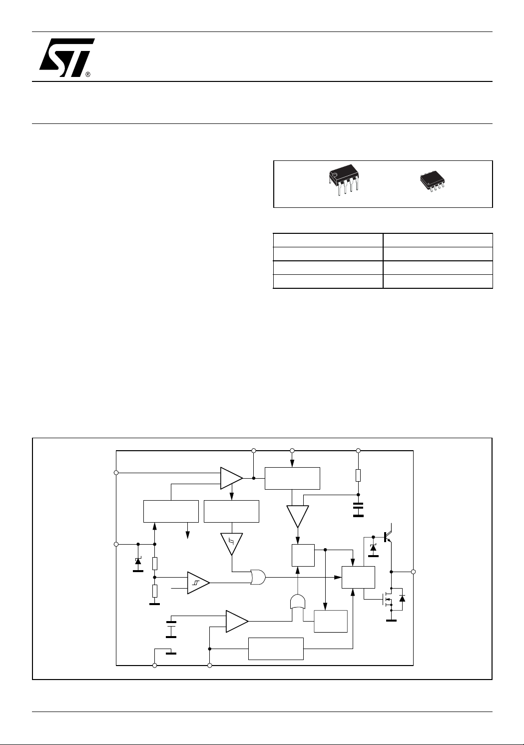
gure 1. Packages
DIP-8
SO-8
Table 1. Order Codes
Part Number Package
L6562N DIP-8
L6562D SO-8
L6562DTR Tape & Reel
DESKTOP PC, MONITOR) UP TO 300W
– HI-END AC-DC ADAPTER/CHARGER
– ENTRY LEVEL SERVER & WEB SERVER
2 DESCRIPTION
The L6562 is a current-mode PFC controller operating in Transition Mode (TM). Pin-to-pin compatible with the predecessor L6561, it offers improved
performance.
COMP MULT CS
23 4
MULTIPLIER AND
THD OPTIMIZER
+
-
5pF
40K
CC
V
June 2004
8
CC
V
25 V
R2
6
2.1 V
1.6 V
GND
R1
INTERNAL
SUPPLY 7V
REF2
V
DRIVER
15 V
7
GD
RSQ
+
UVLO
-
ZERO CURRENT
DETECTOR
+
-
5
ZCD
DISABLE
Starter
stop
STARTER
REV. 6
1/16
Page 2
L6562
2 DESCRIPTION (continued)
The highly linear multiplier includes a special circuit, able to reduce AC input current distortion, that allows
wide-range-mains operation with an extremely low THD, even over a large load range.
The output voltage is contr olled by means of a voltage-mode er ror amplifier and a precise (1% @Tj =
25°C) internal voltage reference.
The device features extremely low consumption (≤70 µA before start-up and <4 mA running) and includes
a disable function s uitable for IC remo te ON/OFF, which makes it easier t o comply with energ y saving
norms (Blue Angel, EnergyStar, Energy2000, etc.).
An effective two-step OVP enab les to sa fely han dle overvol tages either occ urring at start-up or re sulti ng
from load disconnection.
The totem-pole output stage, capable of 600 mA source and 800 mA sink current, is suitable for big MOSFET or IGBT drive which, combined with the other features, makes the device an excellent low-cost solution for EN61000-3-2 compliant SMPS's up to 300W.
Table 2. Absolute Maximum Ratings
Symbol Pin Parameter Value Unit
V
CC
IGD 7 Output Totem Pole Peak Current ±0.8 A
--- 1 to 4 Analog Inputs & Outputs -0.3 to 8 V
IZCD 5 Zero Current Detector Max. Curre nt -50 (source)
P
tot
T
j
T
stg
8 IC Supply voltage (Icc = 20 mA) self-limited V
10 (sink)
Power Dissipation @Tamb = 50°C (DIP-8)
(SO-8)
Junction Temperature Operating range -40 to 150 °C
Storage Temperature -55 to 150 °C
1
0.65
Figure 3. Pin Connection (Top view)
INV
COMP
MULT
CS
1
2
3
4
Vcc
8
7
GD
GND
6
ZCD
5
mA
W
Table 3. Thermal Data
Symbol Parameter SO8 Minidip Unit
2/16
R
th j-amb
Max. Thermal Resistance, Junction-to-ambient 150 100 °C/W
Page 3
Table 4. Pin Description
N° Pin Function
1 INV Inverting input of the error amplifier. The information on the output voltage of the PFC pre-
regulator is fed into the pin through a resistor divider.
2 COMP Output of the erro r amplifier. A compensation ne twork is placed be tween this pin and INV (pin
#1) to achieve stability of the voltage control loop and ensure high power factor and low THD.
3 MULT Main input to the multiplier. This pin is connected to the rect ified mains voltage via a resistor
divider and provides the sinusoidal reference to the current loop.
4 CS Inpu t to th e PW M co mparato r. The current fl owing in the M OSFE T is s ense d thro ugh a resis tor,
the resulting voltage is applied to this pin and compared with an internal sinusoidal-shaped
reference, generated by the multiplier, to determine MOSFET’s turn-off.
5 ZCD Boost inductor’s demagnetization sensing input for transition-mode operation. A negative-going
edge triggers MOSFET’s turn-on.
6 GND Ground. Current return for both the signal part of the IC and the gate driver.
7 GD G ate driver output. The to tem pole output stag e is able to drive power MOSFET’s and IGBT’s
with a peak current of 60 0 mA source and 800 mA sink. The high-level voltage of this pin is
clamped at abou t 12V to avoid excessive gate voltages in case the pin is supplied with a high
Vcc.
8 Vcc Supply Voltage of both the signal par t of the IC and the gate dr iver. The supply voltage upper
limit is extended to 22V min. to provide more he ad roo m for supply voltage cha ng es.
L6562
Table 5. Electrical Characteristics
(T
= -25 to 125°C, VCC = 12, CO = 1 nF; unless otherwise specified)
j
Symbol Parameter Test Condition Min. Typ. Max. Unit
SUPPLY VOLTAGE
V
V
CCon
V
CCOff
Hys Hysteresis 2.2 2.8 V
V
SUPPLY CURRENT
I
start-up
I
MULTIPLIER INPUT
I
MULT
V
MULT
VCS∆
---------------------
∆
V
MULT
ERROR AMPLIFIER
V
I
Operating range After turn-on 10.3 22 V
CC
Turn-on threshold
Turn-off threshold
Zener Voltage ICC = 20 mA 22 25 28 V
Z
(1)
(1)
11 12 13 V
8.7 9.5 10.3 V
Start-up Current Before turn-on, VCC =11V 40 70 µ A
I
Quiescent Current After turn-on 2.5 3.75 mA
q
Operating Supply Current @ 70 kHz 3.5 5 mA
CC
I
Quiescent Current During OVP (either static or
q
Input Bias Current V
dynamic) or V
= 0 to 4 V -1 µA
VFF
=150 mV
ZCD
Linear Operation Range 0 to 3 V
Output Max. Slope V
K
INV
(2)
Gain
Voltage Feedback Input
Threshold
MULT
V
COMP
V
MULT
= 0 to 0.5V
= 1 V, V
= Upper clamp
= 4 V 0.5 0.6 0.7 1/V
COMP
1.65 1.9 V/V
Tj = 25 °C 2.465 2.5 2.535 V
10.3 V < Vcc < 22 V
(1)
2.44 2.56
Line Regulation Vcc = 10.3 V to 22V 2 5 mV
Input Bias Current V
INV
= 0 to 3 V -1 µA
INV
2.2 mA
3/16
Page 4
L6562
Table 5. Electrical Characteristics (continu ed)
= -25 to 125°C, VCC = 12, CO = 1 nF; unless otherwise specified)
(T
j
Symbol Parameter Test Condition Min. Typ. Max. Unit
G
GB Gain-Bandwidth Product 1 MHz
I
COMP
V
COMP
CURRENT SENSE COMPARATOR
I
t
d(H-L)
V
CS clamp
V
CSoffset
ZERO CURRENT DETECTOR
V
ZCDH
V
ZCDL
V
ZCDA
V
ZCDT
I
ZCDb
I
ZCDsrc
I
ZCDsnk
V
ZCDdis
V
ZCDen
I
ZCDres
STARTER
t
START
OUTPUT OVERVOLTAGE
I
OVP
Hys Hysteresis
GATE DRIVER
V
V
V
Oclamp
(1) All param eters are in tr acking
(2) The multipl i er output is given by:
(3) Parameters guaranteed by design, functionality tested in production.
Voltage Gain Open loop 60 80 dB
v
Source Current V
Sink Current V
Upper Clamp Voltage I
Lower Clamp Voltage
Input Bias Current VCS = 0 -1 µA
CS
Delay to Output
Current sense reference clamp V
Current sense offset V
Upper Clamp Voltage I
Lower Clamp Voltage I
Arming Voltage
COMP
COMP
SOURCE
I
= 0.5 mA
SINK
= 4V, V
= 4V, V
= 0.5 mA 5.3 5.7 6 V
= 2.4 V -2 -3.5 -5 mA
INV
= 2.6 V 2.5 4.5 mA
INV
(1)
2.1 2.25 2.4 V
200 350 ns
= Upper clamp 1.6 1.7 1.8 V
COMP
= 0 30 mV
MULT
V
= 2.5V 5
MULT
= 2.5 mA 5.0 5.7 6.5 V
ZCD
= -2.5 mA 0.3 0.65 1 V
ZCD
(3)
2.1 V
(positive-going edge)
Triggering Voltage
(3)
1.6 V
(negative-going edge)
Input Bias Current
= 1 to 4.5 V
V
ZCD
2µA
Source Current Capability -2.5 -5.5 mA
Sink Current Capability 2.5 mA
Disable threshold 150 200 25 0 mV
Restart threshold 350 mV
Restart Current after Disable 30 75 µA
Start Timer period
75 130 300 µs
Dynamic OVP triggering current 35 40 45 µA
(3)
Static OVP threshold
OH
Dropout Voltage
OL
Voltage Fall Time 30 70 ns
t
f
t
Voltage Rise Time 40 80 ns
r
Output clamp voltage I
UVLO saturation V
VcsKV
(1)
I
GDsource
I
GDsource
I
= 200 mA
GDsink
GDsource
= 0 to V
CC
MULTVCOMP
= 20 mA
= 200 mA
= 5mA; Vcc = 20V
, I
CCon
2.5–()⋅⋅=
=10mA 1.1 V
sink
2.1 2.25 2.4 V
10 12 15 V
30 µA
22.6
2.5 3 V
0.9 1.9 V
4/16
Page 5
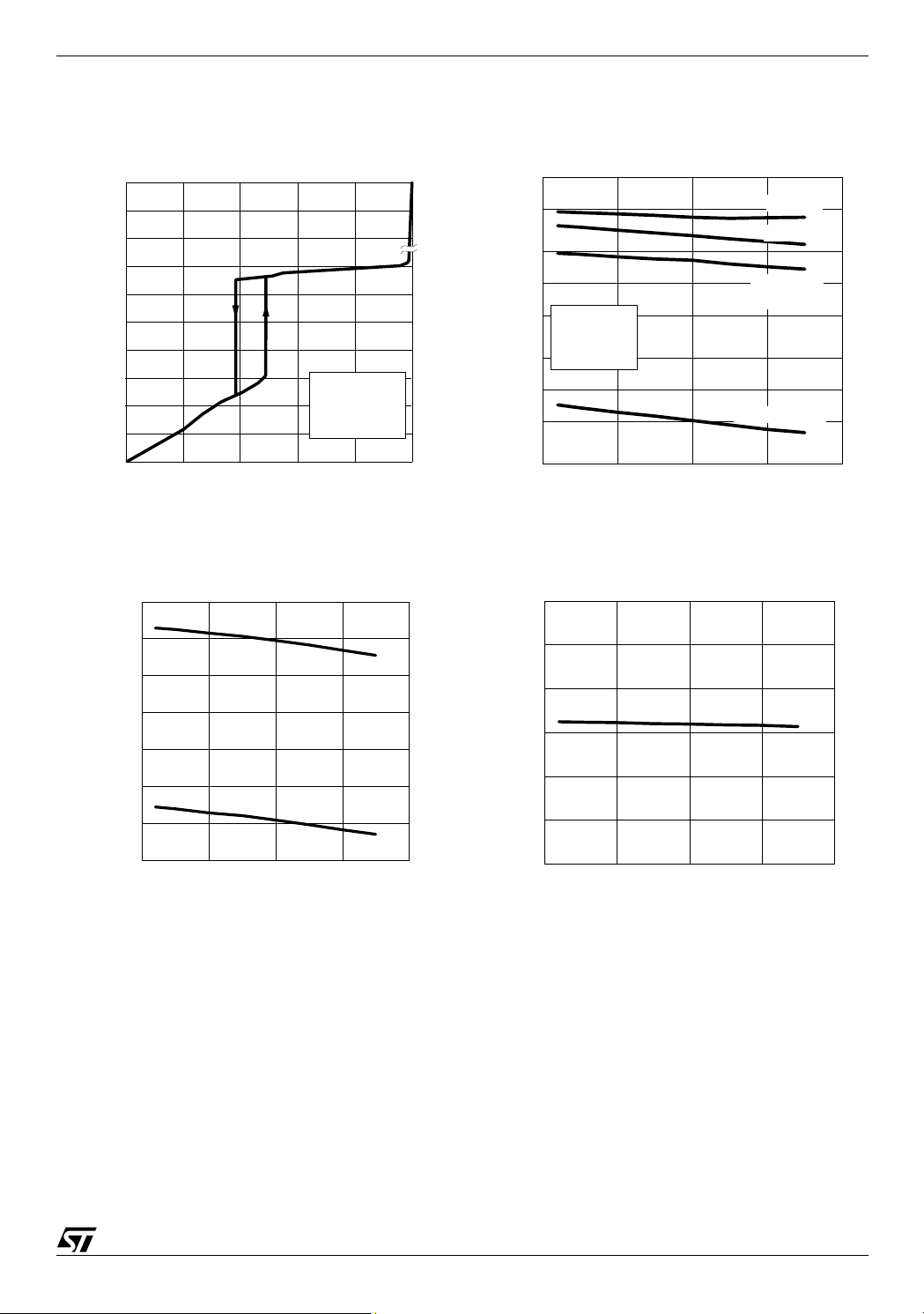
3 TYPICAL ELECTRICAL CHARACTERISTICS
L6562
Figure 4. Supply current vs. Supply voltage
I
CC
(mA)
10
5
1
0.5
0.1
0.05
0.01
0.005
0
0 5 10 15 20
V
cc(V)
Figure 5. Start-up & UVLO vs. T
12.5
V
CC-ON
12
(V)
Co = 1nF
f = 70 kHz
= 25°C
T
j
j
25
Figure 6. IC consumption vs. T
Icc
10
[mA]
5
j
2
1
0.5
Vcc = 12 V
Co = 1 nF
f = 70 kHz
0.2
0.1
0.05
0.02
-50 0 50 100 150
Before start-up
Tj (°C)
Figure 7. Vcc Zener voltage vs. Tj
Vcc
Z
28
(V)
27
Operating
Quiescent
Disabled or
during OVP
CC-OFF
V
(V)
11.5
11
10.5
10
9.5
9
-50 0 50 100 150
Tj (
°C)
26
25
24
23
22
-50 0 50 100 150
Tj (°C)
5/16
Page 6

L6562
Figure 8. Feedback reference vs. Tj
V
REF
2.6
(V)
2.55
2.5
2.45
2.4
-50 0 50 100 150
Tj (°C)
Figure 9. OVP current vs. T
I
OVP
41
(µA)
40.5
40
39.5
39
-50 0 50 100 150
Tj (°C)
j
Vcc = 12 V
Vcc = 12 V
Figure 11. Delay-to-output vs. T
t
D(H-L)
500
(ns)
400
300
200
100
0
-50 0 50 100 150
Tj (°C)
j
Figure 12. Multiplier characteristic
V
(pin 4)
CS
upper voltage
(V)
clamp
1.6
1.4
1.2
1.0
0.8
0.6
0.4
0.2
0
0 0.5 1.0 1.5 2.0 2.5 3.0 3.5 4.0 4.5
5.0
4
5
.
4.0
V
MULT
(pin 3) (V)
Vcc = 12 V
V
COMP
(V)
3.5
3.2
3.0
2.8
2.6
(pin 2)
Figure 10. E/A output clamp levels vs. T
Vpin2
6
(V)
6/16
Upper clamp
5
4
3
Lower clamp
2
-50 0 50 100 150
Tj (°C)
Vcc = 12 V
j
Figure 13. Multiplier gain vs. T
K
1
0.8
j
Vcc = 12 V
=4 V
V
COMP
V
=1V
MULT
0.6
0.4
0.2
0
-50 0 50 100 150
Tj (°C)
Page 7

L6562
Figure 14. Vcs clamp vs. Tj
V
CSx
2
(V)
1.8
1.6
1.4
Vcc = 12 V
V
1.2
COMP = Upper clamp
1
-50 0 50 100 150
Tj (°C)
Figure 15. Start-up timer vs. T
Tstart
150
(µs)
140
130
Vcc = 12 V
Figure 17. ZCD source capability vs. T
I
ZCDsrc
0
(mA)
-2
-4
-6
-8
-50 0 50 100 150
Tj (°C)
j
Figure 18. Gate-drive output low saturation
pin7
V
[V]
4
Tj = 25 °C
Vcc = 11 V
SINK
Vcc = 12 V
= lower clamp
V
ZCD
j
3
120
110
100
-50 0 50 100 150
Tj (°C)
Figure 16. ZCD clamp levels vs. T
V
ZCD
7
(V)
6
5
4
3
2
1
0
-50 0 50 100 150
Tj (°C)
Upper clamp
I
ZCD = ±2.5 mA
Lower clamp
j
Vcc = 12 V
2
1
0
0 200 400 600 800 1,000
IGD[mA]
Figure 19. Gate-drive output high saturation
pin7
V
[V]
-1.5
Tj = 25 °C
Vcc - 2.0
-2.5
Vcc - 2.5
Vcc - 3.0
-3.5
Vcc - 3 .5
Vcc - 4.0
-4.5
-2
-3
-4
0 100 200 300 400 500 600 700
IGD[mA]
Vcc = 11 V
SOURCE
7/16
Page 8

L6562
Figure 20. Gate-drive clamp vs. T
clamp
Vpin7
15
(V)
14
13
12
11
10
-50050100150
Tj (°C)
j
Vcc = 20 V
Figure 21. UVLO saturation vs. T
Vpin7
1.1
(V)
1
0.9
0.8
0.7
0.6
0.5
-50 0 50 100 150
Tj (°C)
j
Vcc = 0 V
4 APPLICATION INFORMATION
4.1 Overvoltage protection
Under steady-state conditions, the voltage control loop keeps the output voltage Vo of a PFC pre-regulator
close to its nomina l v al ue, se t by th e r esi sto rs R1 an d R2 of the outp ut d iv id er. Neglecting ripple co mponents, the current through R1, I
the error amplifier is internally referenced at 2.5V, also the voltage at pin INV will be 2.5V, then:
, equals that through R2, IR2. Considering that the non-inverting input of
R1
I
R2
2.5
------- - I
R2
R1
Vo 2.5–
--------------------- -===
R1
.
If the output voltage experiences an abrupt change ∆Vo > 0 due to a load drop, the voltage at pin INV will
be kept at 2.5V by the loc al feedback of the error amplifier, a network co nnected be tween pins INV a nd
COMP that introduces a long time constant to achieve high PF (this is why ∆Vo can be large). As a result,
the current through R2 will remain equal to 2.5/R2 but that through R1 will become:
R1
Vo 2.5– Vo∆+
--------------------------------------- -=
R1
.
I'
The difference current ∆IR1=I'R1-IR2=I'R1-IR1=∆Vo/R1 will flow through the compensation network and enter the error amplifier output (pin COMP). This current is monitored inside the L6562 and if it reaches about
37 µA the output voltage of the mul tip li er is forced to dec reas e, th us smo othly red ucing the en er gy deliv ered to the output. As the curren t excee ds 40 µA , the O VP is triggered (Dynamic OVP): the ga te- dri ve is
forced low to switch off the external power transistor and the IC put in an idle state. This condition is maintained until the c urrent falls b elow ap prox imatel y 10 µA , w hich re -enab les the in ternal s tarte r and al lows
switching to restart. The output ∆Vo that is able to trigger the Dynamic OVP function is then:
Vo∆ R1 40 10
⋅⋅=
6–
.
An important advan tage of thi s technique is that th e OV le vel can be s et indepe ndently of the regu lated
output voltage: the latter depends on the ratio of R1 to R2, the former on the individual value of R1. Another
advantage is the precision: the tol erance of the detectio n current is 12%, that is 12% tolerance on ∆Vo.
Since ∆Vo << Vo, the tolerance on the absolute value will be proportionally reduced.
Example: Vo = 400 V, ∆Vo = 40 V. Then: R1=4 0V /40 µA=1MΩ; R2=1MΩ·2.5/(400-2.5)=6.289kΩ. The tolerance on the OVP level due to the L6562 will be 40·0.12=4.8V, that is 1.2% of the regulated value.
8/16
Page 9

L6562
When the load of a PFC pre-regulator is very low, the output voltage tends to stay steadily above the nominal value, which cannot be handled by the Dynamic OVP. If this occurs, however, the error amplifier output will saturate low; hence, when this is detected, the external power transistor is switched off and the IC
put in an idle state (Static OVP). Normal operation is resumed as the error amplifier goes back into its linear region. As a result, the L6562 will work in burst-mode, with a repetition rate that can be very low.
When either OVP is activa ted the quies cent co nsump tion of the IC is redu ced to minim ize the dischar ge
of the Vcc capacitor and increase the hold-up capability of the IC supply system.
4.2 THD optimizer circuit
The L6562 is equipped with a special circuit that reduces the conduction dead-angle occurring to the AC
input current near the zero-crossings of the line voltage (crossover distortion). In this way the THD (Total
Harmonic Distortion) of the current is considerably reduced.
A major cause of this distortion is the inability of the system to transfer energy effectively when the instantaneous line voltage is very low. This effect is magnified by the high-frequency filter capacitor placed after
the bridge rectifier, which retains some residual voltage that causes the diodes of the bridge rectifier to be
reverse-biased and the input current flow to temporarily stop.
Figure 22. THD optimization: standard TM PFC controller (left side) and L6562 (right side)
Input current Input current
Rectified mains voltage Rectified mains voltage
Imains
Input current
MOSFET's drain voltage
Vdrain
Imains
Input current
MOSFET's drain voltage
Vdrain
To overcome this issue the ci r cu it emb edd ed in the L656 2 for ce s the PF C pre-r eg ula tor to pr oc ess more
energy near the line voltage zero-crossings as compared to that commanded by the control loop. This will
result in both minimizin g the tim e int er val wher e en ergy tran sfe r is lack in g and ful ly dis c hargi ng the high frequency filter capacito r after the bridge. The effect of the circuit is show n in figure 23, where the key
waveforms of a standard TM PFC controller are compared to those of the L6562.
Essentially, the circuit artificially increases the ON-time of the power switch with a positive offset added to
9/16
Page 10

L6562
the output of the multiplier in the proximity of the line voltage zero-crossings. This offset is reduced as the
instantaneous line vol tage inc reases , so that it becomes neglig ible as the l ine vol tage mo ves towa rd the
top of the sinusoid.
To maximally benefit from the THD optimizer circuit, the high-frequency filter capacitor after the bridge rectifier should be minimi zed, comp atibly with EM I filter ing nee ds. A la rge capac itanc e, in fact, i ntrodu ces a
conduction dead-angle of the AC input current in itself - even with an ideal energy transfer by the PFC preregulator - thus making the action of the optimizer circuit little effective.
Figure 23. Typical application circuit (250W, Wide-range mains)
D3 1N5406
Ω
5
L6562
T
R50 10 kΩ
C3 2.2 µF
C23
680 nF
21
7
4
6
STTH5L06
R7
Ω
10
0.33
R9
1W
Ω
STP12NM50
7 °C/W heat sink
R10
0.33
1W
MOS
Ω
2.5 Ω
R13
9.53 k
Ω
NTC
D1
R11
750 k
R12
750 k
Ω
Ω
Vo=400V
Po=250W
C6
100 µF
450V
-
5A/250V
Vac
(85V to 265V)
FUSE
+
-
BRIDGE
STBR606
C1
1 µF
400V
22 k
R4
R5
D8
1N4150
D2
1N5248B
C5 12 nF
C4
100 nF
R14
100
R6
68 kΩ
8
3
180 kΩ
1.5 MΩ
1.5 M
10nF
R3
Ω
Ω
180 k
R1
R2
Ω
C2
C29
22 µF
25V
Boost Inductor Spec: EB0057-C (COILCRAFT)
Figure 24. Demo board (EVAL6562-80W, Wide-range mains): Electrical schematic
T
C23
330 nF
5
21
L6562
6
R50 12 kΩ
C3 680 nF
4
D1
STTH1L06
R7
33
Ω
7
R9
0.82
0.6 W
STP8NM50
Ω
MOS
R10
0.82
0.6 W
Ω
9.53 k
4A/250V
Vac
(85V to 265V)
FUSE
R4
180 kΩ
R1
750 kΩ
BRIDGE
DF06M
+
-
Boost Inductor Spec (ITACOIL E2543/E)
C1
0.47 µF
400V
R2
750 k
Ω
C2
10nF
R3
10 k
Ω
E25x13x7 core, 3C85 ferrite
1.5 mm gap for 0.7 mH primary inductance
Primary: 105 turns 20x0.1 mm
Secondary: 11 turns 0.1 mm
180 k
22 µF
R5
C29
25V
Ω
D8
1N4150
D2
1N5248B
C5 12 nF
C4
100 nF
R14
100 Ω
R6
68 kΩ
8
3
NTC
2.5 Ω
R13
Vo=400V
R11
Po=80W
750 k
Ω
R12
Ω
750 k
C6
47 µF
450V
Ω
-
10/16
Page 11

Figure 25. EVAL6562-80W: PCB and component layout (Top view, real size: 57 x 108 mm)
L6562
Table 6. EVAL6562N: Evaluation results at full load
Vin (VAC)
Pin (W)
85 86.4 394.79 12.8 80.16 92.8 0.998 3.6
110 84.6 394.86 12.8 80.20 94.8 0.996 4.2
135 83.8 394.86 12.8 80.20 95.7 0.991 4.9
175 83.2 394.87 15.5 80.20 96.4 0.981 6.5
220 82.9 394.87 15.7 80.20 96.7 0.956 7.8
265 82.7 394.87 15.9 80.20 97.0 0.915 9.2
Note: measurements done with the line filter shown in figure 23
Vo (VDC) ∆Vo(V
pk-pk
)
Po (W) η (%) PF THD (%)
Table 7. EVAL6562N: Evaluation results at half load
Vin (VAC)
Pin (W)
85 42.8 394.86 6.6 40.20 93.9 0.994 5.5
110 42.5 394.90 6.6 40.20 94.6 0.985 6.2
135 42.5 394.91 6.7 40.20 94.6 0.967 7.1
175 42.5 394.93 8.0 40.19 94.6 0.939 8.3
Vo (VDC) ∆Vo(V
pk-pk
)
Po (W) η (%) PF THD (%)
220 42.6 394.94 8.2 40.19 94.3 0.869 9.8
265 42.6 394.94 8.3 40.19 94.3 0.776 11.4
Note: measurements done with the line filter shown in figure 23
11/16
Page 12

L6562
Table 8. EVAL6562N: No-load measurements
Vin (VAC)
Pin (W)
Vo (VDC) ∆Vo(V
pk-pk
)
85 0.4 396.77 0.45 0
110 0.3 396.82 0.55 0
135 0.3 396.83 0.60 0
(*)
175
(*)
220
(*)
265
(*)
Vcc = 12V supplied externally
0.4 396.90 1.00 0
0.4 396.95 1.40 0
0.5 396.98 1.65 0
Figure 26. Line filter (not tested for EMI compliance) used for EVAL6562N evaluation
to the AC
source
B81133
470 nF, X2
EPCOS
B82732
47 mH, 1.3A
EPCOS
B81133
680 nF, X2
EPCOS
to
EVAL6562N
Po (W)
12/16
Page 13

Figure 27. DIP-8 Mechanical Data & Package Dimensions
L6562
DIM.
mm inch
MIN. TYP. MAX. MIN. TYP. MAX.
A3.32 0.131
a1 0.51 0.020
B 1.15 1.65 0.045 0.065
b 0.356 0.55 0.014 0.022
b1 0.204 0.304 0.008 0.012
D 10.92 0.430
E 7.95 9.75 0.313 0.384
e2.54 0.100
e3 7.62 0.300
e4 7.62 0.300
F 6.6 0.260
I 5.08 0.200
L 3.18 3.81 0.125 0.150
Z 1.52 0.060
OUTLINE AND
MECHANICAL DATA
DIP-8
13/16
Page 14

L6562
Figure 28. SO-8 Mechanical Data & Package Dimensions
DIM.
A 1.35 1.75 0.053 0.069
A1 0.10 0.25 0.004 0.010
A2 1.10 1.65 0.043 0.065
B 0.33 0.51 0.013 0.020
C 0.19 0.25 0.007 0.010
(1)
D
E 3.80 4.00 0.15 0.157
e 1.27 0.050
H 5.80 6.20 0.228 0.244
h 0.25 0.50 0.010 0.020
L 0.40 1.27 0.016 0.050
k 0˚ (min.), 8˚ (max.)
ddd 0.10 0.004
Note: (1) Dimensi ons D does not inclu de mold flash, pro tru-
mm inch
MIN. TYP. MAX. MIN. TYP. MAX.
4.80 5.00 0.189 0.197
sions or gate bur rs.
Mold flash , pot rus ions or ga t e burr s shall not exce ed
0.15mm (.006inch) in total (both side).
OUTLINE AND
MECHANICAL DA T A
SO-8
14/16
0016023 C
Page 15

Table 9. Revision History
Date Revision Description of Chan g es
January 2004 5 First Issue
L6562
June 2004 6 Modified the Style-look in compliance with the “Corporate Technical
Publications Design Guide ”.
Changed input of the power amplifier connected to Multiplier (Fig. 2).
15/16
Page 16

L6562
Information furnished is believed to be accurate and reliable. However, STMicroelectronics assumes no responsibility for the consequences
of use of such information nor for any infri ngement of patents or othe r rights of third parties whic h may result from its use. No license is granted
by implication or otherwise under any patent or patent rights of STMicroelectronics. Specifications mentioned in this publication are subject
to change without no tice. This publication supersedes and replaces all information previously suppl ied. STMicroelectronics product s are not
authorized for use as criti cal components in life support devices or systems without express written approval of STMicroelectronics.
The ST logo is a registered trademark of STMicroelectronics.
All other names are the property of their respective owners
© 2004 STMicroelectronics - All rights reserved
Australia - Belgium - Brazil - Canada - China - Czech Republic - Finland - France - Germany - Hong Kong - India - Israel - Italy - Japan -
Malaysia - Malta - Morocco - Singapore - Spain - Sweden - Switzerland - United Kingdom - United States
STMicroelectronics GROUP OF COMPANIES
www.st.com
16/16
 Loading...