

STMicroelectronics L6561, L6561D, LD7530NPN Schematics

L6561
Fi
POWER FACTOR CORRECTOR
1 FEATURES
■ VERY PRECISE ADJUSTABLE OUTPUT
OVERVOLTAGE PROTECTION
■ MICRO POWER START-UP CURRENT (50µA
TYP.)
■ VERY LOW OPERATING SUPPLY
CURRENT(4mA TYP.)
■ INTERNAL START-UP TIMER
■ CURRENT SENSE FILTER ON CHIP
■ DISABLE FUNCTION
■ 1% PRECISION (@ T
= 25°C) INTERNAL
j
REFERENCE VOLTAGE
■ TRANSITION MODE OPERATION
■ TOTEM POLE OUTPUT CURRENT: ±400mA
■ DIP-8/SO-8 PACKAGES
2 DESCRIPTION
L6561 is the improv ed versi on of the L 6560 stan dard Power Factor Corrector. Fully compatible
with the standard version, it has a superior performant multiplier making the device capable of working in wide input voltage range application s (from
85V to 265V) with an ex ce ll ent T HD. Fur th er more
the start up current has be en red uced at f ew tens
of mA and a disable function has been implemented on the ZCD pin, guaranteeing lower current
consumption in stand by mode.
gure 1. Packages
DIP-8
SO-8
Table 1. Order Codes
Part Number Package
L6561 DIP-8
L6561D SO-8
L6561D013TR Tape & Reel
Realised in mixed BCD technology, the chip gives
the following benefits:
– micro power start up current
– 1% precision internal reference voltage
– (Tj = 25°C)
– S oft Output Over Voltage Protection
– no need for external low pass filter on the cur-
rent sense
– v ery low operating quiescent current minimis-
es power dissipation
The totem pole ou tput stage is capable of driving
a Power MOS or IGBT with source and sink currents of ±400mA. The device is ope rating in transition mode and it is optimised for Electronic Lamp
Ballast application, AC-DC adaptors and SMPS.
Figure 2. Block Diagram
INV
V
June 2004
COMP MULT CS
1
VOLTAGE
REGULATOR
8
CC
20V
R1
R2
2.1V
1.6V
6
GND
INTERNAL
SUPPLY 7V
+
-
V
REF2
2.5V
5
ZCD
23 4
+
OVER-VOLTAGE
DETECTION
UVLO
+
-
ZERO CURRENT
DETECTOR
DISABLE
MULTIPLIER
-
RSQ
+
STARTER
5pF
40K
DRIVER
D97IN547E
V
CC
7
GD
REV. 16
1/13

L6561
Table 2. Absolute Maximum Ratings
Symbol Pin Parameter Value Unit
I
Vcc
I
GD
INV , COMP
MULT
CS 4 Current Sense Input -0.3 to 7 V
ZCD 5 Zero Current Detector 50 (source)
P
tot
T
j
T
stg
Figure 3. Pin Connection (Top view)
8Iq + IZ; (IGD = 0) 30 mA
7 Output Totem Pole Peak Current (2µs) ±700 mA
1, 2, 3 Analog Inputs & Outputs -0.3 to 7 V
-10 (sink)
Power Dissipation @T
Junction Temperature Operating Range -40 to 150 °C
Storage Temperature -55 to 150 °C
= 50 °C (DIP-8)
amb
(SO-8)
1
0.65
mA
mA
W
W
INV
COMP
MULT
CS
1
2
3
4ZCD
DIP8
8
7
6
5
V
CC
GD
GND
Table 3. Thermal Data
Symbol Parameter SO 8 MINIDIP Unit
R
th j-amb
Thermal Resistance Junction to ambient 150 100 °C/W
Table 4. Pin Description
N. Name Function
1 INV Inverting input of the error amplifier. A resistive divider is connected between the output
2 COMP Output of error amplifier. A feedback compensation network is placed between this pin and the
3 MULT Input of the multiplier stage. A resistive divider connects to this pin the rectified mains. A voltage
4 CS Input to the comparator of the control loop. The curren t is sense d by a resisto r and the resulti ng
5 ZCD Zero current detection input. If it is connected to GND, the device is disabled.
6 GND Current return for driver and control circuits.
7 GD Gate driver output. A pu sh pul l ou tpu t st ag e is a ble to drive the Power MOS with peak current of
8V
(1) Parameter guaranteed by design, not tested in production.
regulated voltage and this point, to provide voltage feedback.
INV pin.
signal, proportional to the rectified mains, appears on this pin.
voltage is applied to this pin.
400mA (source and sink).
Supply voltage of driver and control circuits.
CC
2/13

L6561
Table 5. Electrical Characteristics
= 14.5V; T
(V
CC
Symbol Pin Parameter Test Condition Min. Typ. Max. Unit
SUPPLY VOLTAGE SECTION
V
V
CC ON
V
CC OFF
CC
8 Operating Range after turn-on 11 18 V
8 Turn-on Threshold 11 12 13 V
8 Turn-off Threshold 8.7 9.5 10.3 V
Hys 8 Hysteresis 2.2 2.5 2.8 V
SUPPLY CURRENT SECTION
I
START-U
I
q
I
CC
8 Start-up Current before turn-on (VCC =11V) 205090µA
8 Quiescent Current 2.6 4 mA
8 Operating Supply Current CL = 1nF @ 70KHz 4 5.5 mA
Iq 8 Quiescent Current V
8V
V
Z
8 Zener Voltage ICC = 25mA 18 20 22 V
ERROR AMPLIFIER SECTION
V
INV
I
INV
G
V
1 Voltage Feedback Input
1 Input Bias Current -0.1 -1 µA
GB Gain Bandwidth 1 MHz
I
COMP
V
COMP
2 Source Current V
2 Upper Clamp Voltage I
MULTIPLIER SECTION
V
MULT
VCS∆
-----------------
∆
V
mult
3 Linear Operating Voltage 0 to 3
KGain V
CURRENT SENSE COM PARATOR
V
I
CS
t
d (H-L)
CS
4 Current Sense Reference
4 Input Bias Current VOS = 0 -0.05 -1 µA
4 Delay to Output 200 450 ns
4 Current Sense Offset 0 15 mV
ZERO CURRENT DETECTOR
V
V
V
ZCD
ZCD
ZCD
5 Input Thre shold Voltage Rising
5 Upper Clamp Voltage I
5 Upper Clamp Voltage I
= -25°C to 125°C;unless otherwise specified)
amb
= 2.7V 1.4 2.1 mA
pin1
off
CC off
20 50 90 µA
1.4 2.1 mA
Threshold
Line Regulation V
in OVP condition V
≤150mV, VCC > VCC
PIN5
≤ 150mV, VCC < V
PIN5
T
= 25°C 2.465 2.5 2.535 V
amb
12V < V
CC
< 18V 2.44 2.56 V
CC
= 12 to 18V 2 5 mV
Voltage Gain Open loop 60 80 dB
Sink Current V
Lower Clamp Voltage I
= 4V, V
COMP
= 4V, V
COMP
= 0.5mA 5.8 V
SOURCE
= 0.5mA 2.25 V
Sink
= 2.4V -2 -4 -8 mA
INV
= 2.6V 2.5 4.5 mA
INV
0 to 3.5
Output Max. Slope V
Clamp
= from 0V to 0.5V
MULT
V
= Upper Clamp Voltage
COMP
= 1V V
MULT
V
= 2.5V
MULT
V
= Upper Clamp Voltage
COMP
= 4V 0.45 0.6 0.75 1/V
COMP
1.65 1.9
1.6 1.7 1.8 V
(1) 2.1 V
Edge
Hysteresis (1) 0.3 0.5 0.7 V
= 20µA4.55.15.9V
ZCD
= 3mA 4.7 5.2 6.1 V
ZCD
V
3/13
L6561
Table 5. Electrical Characteristics (continued)
= 14.5V; T
(V
CC
Symbol Pin Parameter Test Condition Min. Typ. Max. Unit
V
ZCD
I
ZCD
I
ZCD
I
ZCD
V
DIS
I
ZCD
OUTPUT SECTION
V
GD
t
r
t
f
I
GD off
OUTPUT OVERVOLTAGE SECTION
I
OVP
RESTART TIMER
t
START
5 Lower Clamp Voltage I
5 Sink Bias Current 1V ≤ V
5 Source Current Capability -3 -10 mA
5 Sink Current Capability 3 10 mA
5 Disable threshold 150 200 250 mV
5 Restar t Cu rre nt Aft er Dis able V
7 Dropout Voltage I
7 Output Voltage Rise Time CL = 1nF 40 100 ns
7 Output Voltage Fall Time CL = 1nF 40 100 ns
7 IGD Sink Current VCC =3.5V VGD = 1V 5 10 - mA
2 OVP Triggering Current 35 40 45 µA
= -25°C to 125°C;unless otherwise specified)
amb
= -3mA 0.3 0.65 1 V
ZCD
≤ 4.5V 2 µA
ZCD
< V
ZCD
GDsource
I
GDsource
I
GDsink
I
GDsink
Static OVP Threshold 2.1 2.25 2.4 V
Start Timer 70 150 400 µs
; VCC > V
dis
= 200mA 1.2 2 V
= 20mA 0.7 1 V
= 200mA 1.5 V
= 20mA 0.3 V
CCOFF
-100 -200 -300 µA
3 OVER VOLTAGE PROTECTION OVP
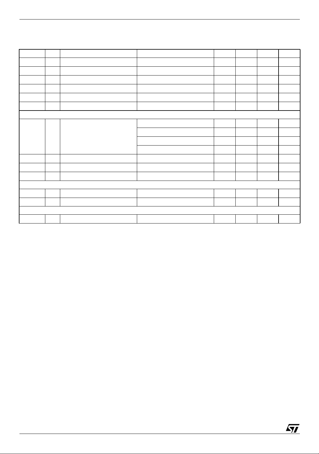
The output voltage is expected to be kept by the opera tion of the PFC circui t close to it s nomi nal value.
This is set by the r atio of the t wo exte rnal r esistors R1 and R2 (see fig . 5), tak ing i nto co nsider ation t hat
the non inverting input of the error amplifier is biased inside the L6561 at 2.5V.
In steady state conditions, the current through R1 and R2 is:
V
2.5–
out
I
R1sc
------------------------- - I
R1
and, if the external compensation network is made only with a capacitor C
equals zero.When the output voltage increases abruptly the current through R1 becomes:
V
I
R1
outsc
----------------------------------------------------- I
Since the current through R2 does not change, ∆I
V
2.5–∆+
out
R1
must flow through the capacitor C
R1
error amplifier.
This current is monitored inside the L6561 and when reaches about 37µA the output volt a ge of th e mu lti-
plier is forced to decrease, thu s redu ci ng th e ener g y drawn fro m the ma ins . If the curr ent exceed s 40µA,
the OVP protection is triggered (Dynamic OVP), and the external power transistor is switched off until the
current falls approximately below 10µA.
However, if the over voltage persists, an interna l comparator (Static OVP) confirms the OVP conditi on
keeping the external power swi tch turned off (see fig. 4).Finally, the overv oltage that triggers the OVP
function is:
∆V
= R1 · 40µA.
out
Typical values for R
, R2 and C are shown in the application circuits. The overvoltage can be set indepen-
1
R2
R1scIR1
2.5V
------------===
R2
∆+==
, the current through C
comp
comp
comp
and enter the
4/13
L6561
dently from the average output voltage. The precision in setting the overvoltage threshold is 7% of the overvoltage value (for instance ∆V = 60V ± 4.2V).
3.1 Disable function
The zero current detector (ZCD) pin can be used for device disabling as well. By grounding the ZCD voltage the device is disabled reducing the supply current consumption at 1.4mA typical (@ 14.5V supply voltage).
Releasing the ZCD pin the internal start-up timer will restart the device.
Figure 4.
OVER VOLTAGE
V
OUT nominal
40µA
10µA
I
SC
E/A OUTPUT
2.25V
DYNAMIC OVP
STATIC OVP
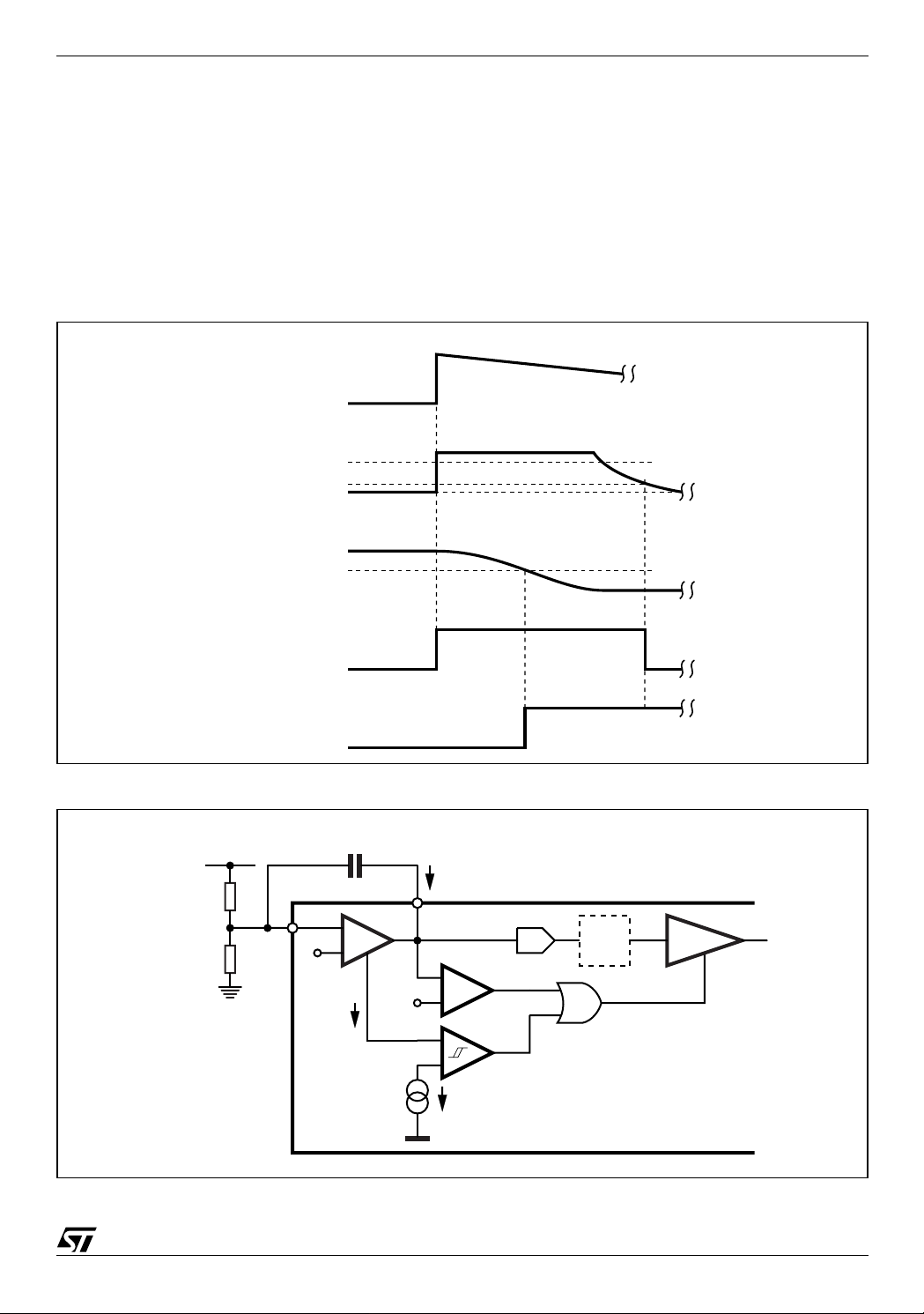
Figure 5. Overvoltage Protection Circuit
Ccomp.
+Vo
R1
1
-
E/A
R2
D97IN591
+
2.5V
∆I
40µA
2.25V
D97IN592A
∆I
2
X PWM DRIVER
-
+
5/13
 Loading...