

STMicroelectronics L6201, L6201PS, L6202, L6203 Schematics
L6201
®
SUPPLY VOLTAGE UP TO 48V
5A MAX PEAK CU RRENT (2A max. for L6201)
TOTAL RMS CURRENT UP TO
L6201: 1A; L6202: 1.5A; L6203/L6201PS: 4A
R
0.3 Ω (typical value at 25 °C)
DS (ON)
CROSS CONDUCTION PRO TECTION
TTL COMPATIBLE DRIVE
OPERATING FREQUENCY UP TO 100 KHz
THERMAL SHUTDOWN
INTERNAL LOGIC SUPPLY
HIGH EFFICIENCY
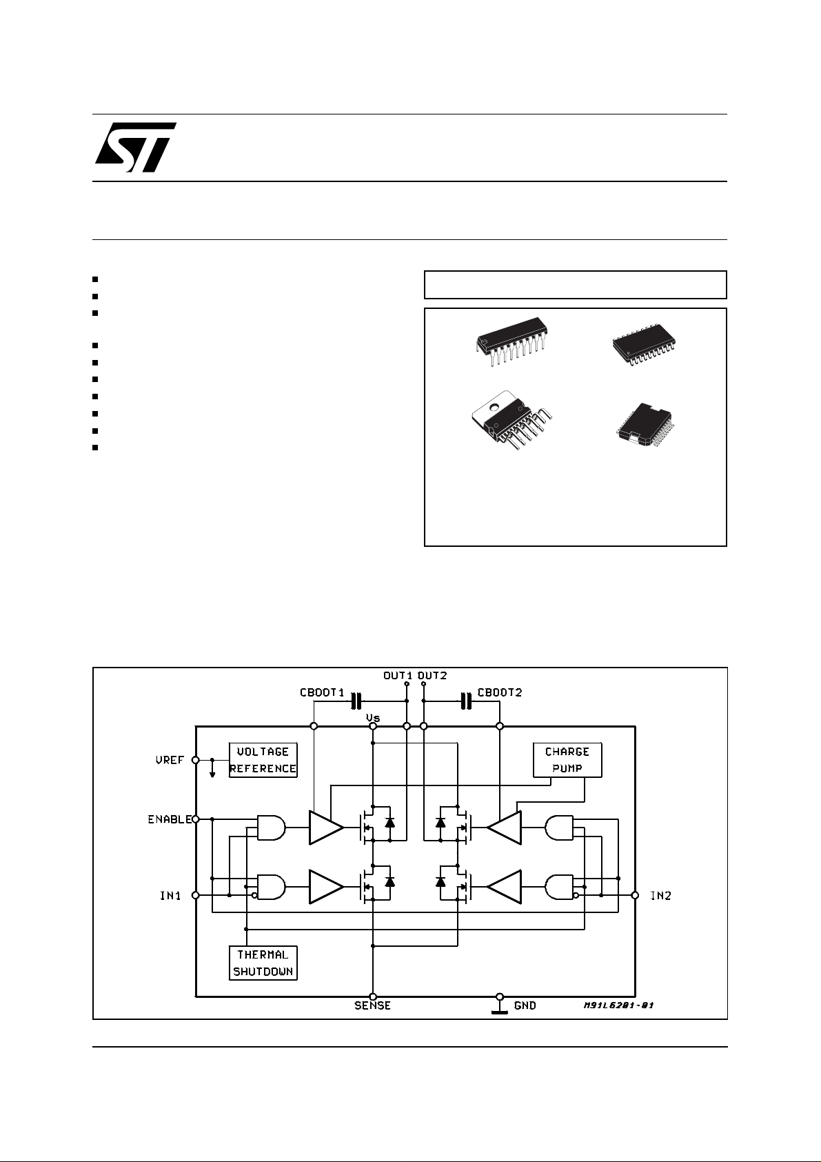
DESCRIPTION
The I.C. is a full bridge driver for motor control applications realized in Multipower-BCD technology
which combines isolated DMOS power transistors
with CMOS and Bipolar circuits on the same chip.
By using mixed technology it has been possible to
optimize the logic circuitry and the power stage to
achieve the best possible performance. The
DMOS output transistors can operate at supply
voltages up to 42V and efficiently at high switch-
L6202 - L6203
DMOS FULL BRIDGE DRIVER
MULTIPOWER BCD TECHNOLOGY
Powerdip 12+3+3
Multiwatt11
ORDERING NUMBERS:
L6201
L6201PS
L6202
L6203
ing speeds. All the logic inputs are TTL, CMOS
and µC compatible. Each channel (half-bridge) of
the device is controlled by a separate logic input,
while a common enable controls both channels.
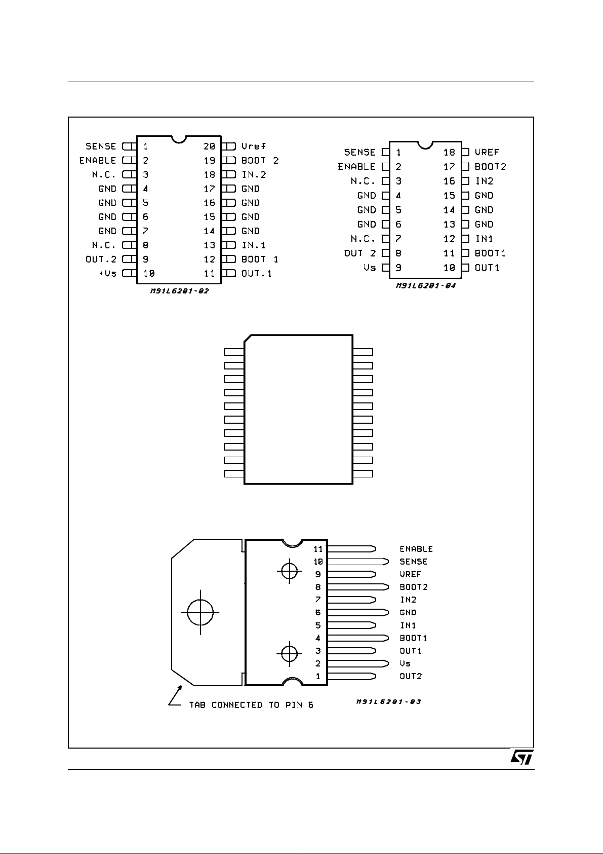
The I.C. is mounted in three different packages.
SO20 (12+4+4)
PowerSO20
(SO20)
(PowerSO20)
(Powerdip18)
(Multiwatt)
BLOCK DIAGRAM
July 2003
This is advanced information on a new product now in development or undergoing evaluation. Details are subject to change without notice.
1/20
L6201 - L6202 - L6203
PIN CONNECTIONS
(Top view)
SO20
GND
N.C.
N.C.
OUT2
OUT1
BOOT1
N.C.
GND 10
V
IN1
POWERDIP
1
2
3
4
S
5
6
7
8
9
D95IN216
20
19
18
17
16
15
14
13
12
11
GND
N.C.
N.C.
ENABLE
SENSE
Vref
BOOT2
IN2
N.C.
GND
2/20
PowerSO20
MULTIWATT11
PINS FUNCTIONS
L6201 - L6202 - L6203
Device
L6201 L6201PS L6202 L6203
1 16 1 10 SENSE A resistor R
Name Function
connected to this pin provides feedback for
sense
motor current control.
2 17 2 11 ENABLEWhen a logic high is present on this pin the DMOS POWER
transistors are enabled to be selectively driven by IN1 and IN2.
3 2,3,9,12,
3 N.C. Not Connected
18,19
4,5 – 4
– 1, 10 5 GND Common Ground Terminal
GND Common Ground Terminal
6
6,7 – 6 GND Common Ground Terminal
8 – 7 N.C. Not Connected
9 4 8 1 OUT2 Ouput of 2nd Half Bridge
10 5 9 2 V
s
Supply Voltage
11 6 10 3 OUT1 Output of first Half Bridge
12 7 11 4 BOOT1 A boostrap capacitor connected to this pin ensures efficient
driving of the upper POWER DMOS transistor.
13 8 12 5 IN1 Digital Input from the Motor Controller
14,15 – 13
– 11, 20 14 GND Common Ground Terminal
GND Common Ground Terminal
6
16,17 – 15 GND Common Ground Terminal
18 13 16 7 IN2 Digital Input from the Motor Controller
19 14 17 8 BOOT2 A boostrap capacitor connected to this pin ensures efficient
driving of the upper POWER DMOS transistor.
20 15 18 9 V
ref
Internal voltage reference. A capacitor from this pin to GND is
recommended. The internal Ref. Voltage can source out a
current of 2mA max.
ABSOLUTE MAXIMUM RATINGS
Symbol Parameter Value Unit
V
V
OD
V
, V
IN
I
o
V
sense
V
P
tot
, TjStorage and Junction Temperature – 40 to + 150 °C
T
stg
Note 1:
Note 2:
Power Supply 52 V
s
Differential Output Voltage (between Out1 and Out2) 60 V
Input or Enable Voltage – 0.3 to + 7 V
EN
Pulsed Output Current for L6201PS/L6202/L6203 (Note 1)
– Non Repetitive (< 1 ms) for L6201
for L6201PS/L6202/L6203
DC Output Current for L6201 (Note 1)
5
5
10
1
Sensing Voltage – 1 to + 4 V
Boostrap Peak Voltage 60 V
b
Total Power Dissipation:
= 90°C for L6201
T
pins
for L6202
= 90°C for L6201PS/L6203
T
case
= 70°C for L6201 (Note 2)
T
amb
for L6202 (Note 2)
for L6201PS/L6203 (Note 2)
Pulse width limited only by junction temperature and transient thermal impedance (see thermal characteristics)
Mounted on board with minimized dissipating copper area.
4
5
20
0.9
1.3
2.3
A
A
A
A
W
W
W
W
W
W
3/20
L6201 - L6202 - L6203
THERMAL DATA
Symbol Parameter
Rt
h j-pins
Rt
h j-case
Rt
h j-amb
(*) Mounted on aluminium substrate.
Thermal Resistance Junction-pins max
Thermal Resistance Junction Case max.
Thermal Resistance Junction-ambient max.
ELECTRICAL CHARACTERISTICS
L6201 L6201PS L6202 L6203
15
–
85
(Refer to the Test Circuits; T
Value
–
–
13 (*)
= 25°C, VS = 42V, V
j
12
–
60
–
3
35
= 0, unless
sens
otherwise specified).
Symbol Parameter Test Conditions Min. Typ. Max. Unit
V
s
V
ref
I
REF
I
s
f
c
T
j
T
d
Supply Voltage 12 36 48 V
Reference Voltage I
= 2mA 13.5 V
REF
Output Current 2mA
Quiescent Supply Current EN = H VIN = L
EN = H V
EN = L ( Fig. 1,2,3)
= H
IN
IL = 0
10
10
8
15
15
15
Commutation Frequency (*) 30 100 KHz
Thermal Shutdown 150 °C
Dead Time Protection 100 ns
TRANSISTORS
OFF
I
DSS
Leakage Current Fig. 11 Vs = 52 V 1 mA
ON
R
V
DS(ON)
V
DS
sens
On Resistance Fig. 4,5 0.3 0.55 Ω
Drain Source Voltage Fig. 9
I
DS
I
DS
I
DS
= 1A
= 1.2A
= 3A
L6201
L6202
L6201PS/0
3
0.3
0.36
0.9
Sensing Voltage – 1 4 V
SOURCE DRAIN DIODE
Unit
°C/W
mA
mA
mA
V
V
V
V
sd
t
rr
t
fr
Forward ON Voltage Fig. 6a and b
Reverse Recovery Time
Forward Recovery Time 200 ns
LOGIC LEVELS
V
V
I
4/20
IN L
IN H
I
IN L
IN H
, V
, V
, I
, I
Input Low Voltage – 0.3 0.8 V
EN L
Input High Voltage 2 7 V
EN H
Input Low Current VIN, VEN = L –10 µA
EN L
Input High Current VIN, VEN = H 30 µA
EN H
= 1A
I
SD
= 1.2A
I
SD
= 3A
I
SD
L
dif
= 25 A/µs
dt
I
= 1A
F
= 1.2A
I
F
= 3A
I
F
L6201
EN = L
L6202
EN = L
L6201PS/03
EN =
L6201
L6202
L6203
0.9 (**)
0.9 (**)
1.35(**)
300 ns
V
V
V
L6201 - L6202 - L6203
ELECTRICAL CHARACTERISTICS
(Continued)
LOGIC CONTROL TO POWER DRIVE TIMING
Symbol Parameter Test Conditions Min. Typ. Max. Unit
t
(Vi) Source Current Turn-off Delay Fig. 12 300 ns
1
t
(Vi) Source Current Fall Time Fig. 12 200 ns
2
t
(Vi) Source Current Turn-on Delay Fig. 12 400 ns
3
t
(Vi) Source Current Rise Time Fig. 12 200 ns
4
t
(Vi) Sink Current Turn-off Delay Fig. 13 300 ns
5
t
(Vi) Sink Current Fall Time Fig. 13 200 ns
6
t
(Vi) Sink Current Turn-on Delay Fig. 13 400 ns
7
t
(Vi) Sink Current Rise Time Fig. 13 200 ns
8
(*)
Limited by power dissipation
(**)
In synchronous rectification the drain-source voltage drop VDS is shown in fig. 4 (L6202/03); typical value for the L6201 is of 0.3V.
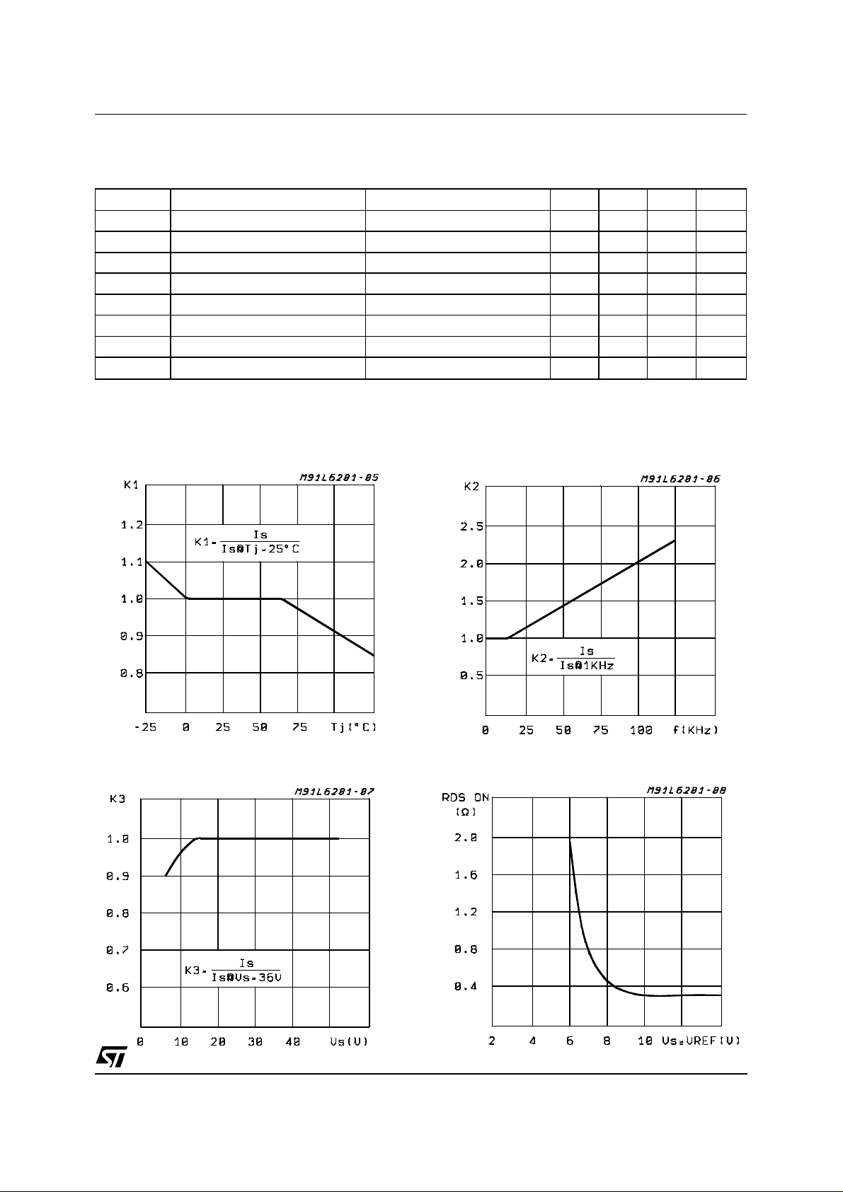
Figure 1:
Typical Normalized I
vs. T
S
j
Figure 2:
Typical Normalized Quiescent Current
vs. Frequency
Figure 3:
Typical Normalized I
vs. V
S
S
Figure 4:
Typical R
DS (ON)
vs. VS ~ V
ref
5/20
L6201 - L6202 - L6203
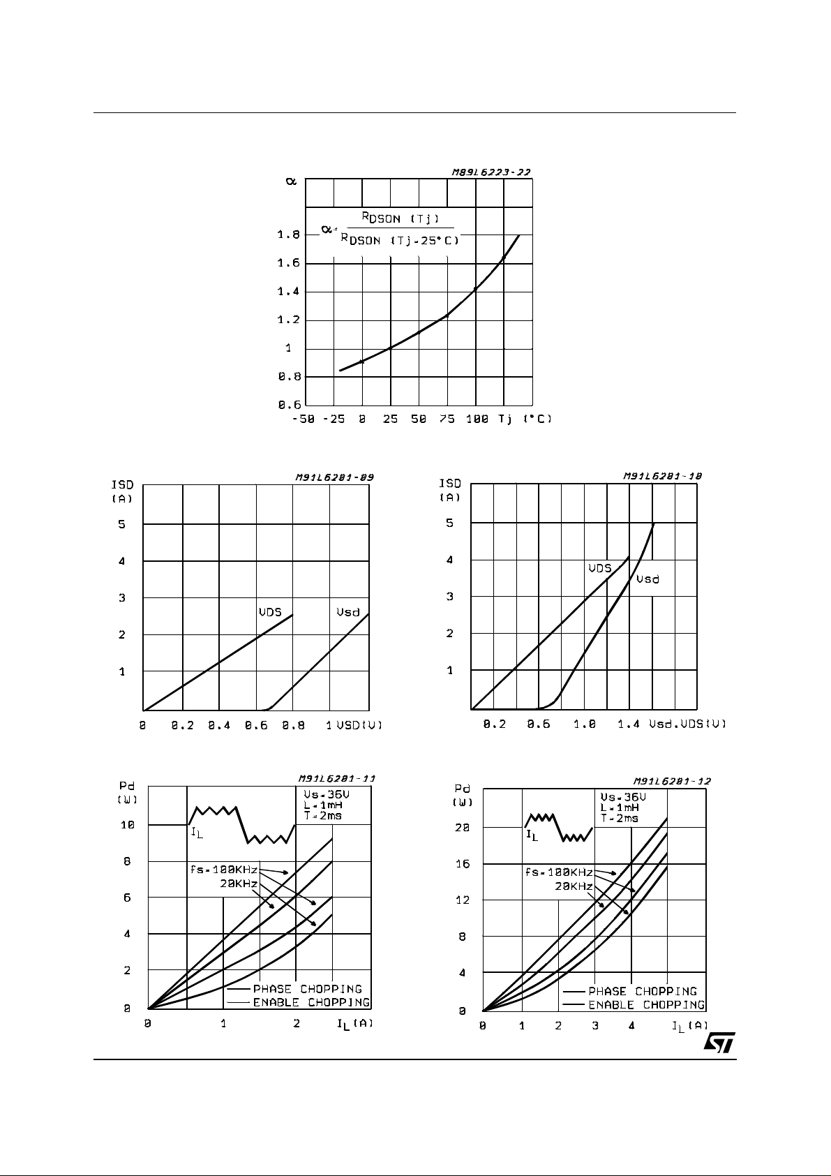
Figure 5:
Figure 6a:
Normalized R
at 25°C vs. Temperature Typical Values
DS (ON)
Typical Diode Behaviour in Synchro-
nous Rectification (L6201)
Figure 6b:
Typical Diode Behaviour in Synchro-
nous Rectification (L6201PS/02/03)
Figure 7a:
6/20
Typical Power Dissipation vs I
(L6201)
L
Figure 7b:
Typical Power Dissipation vs I
L
(L6201PS, L6202, L6203))
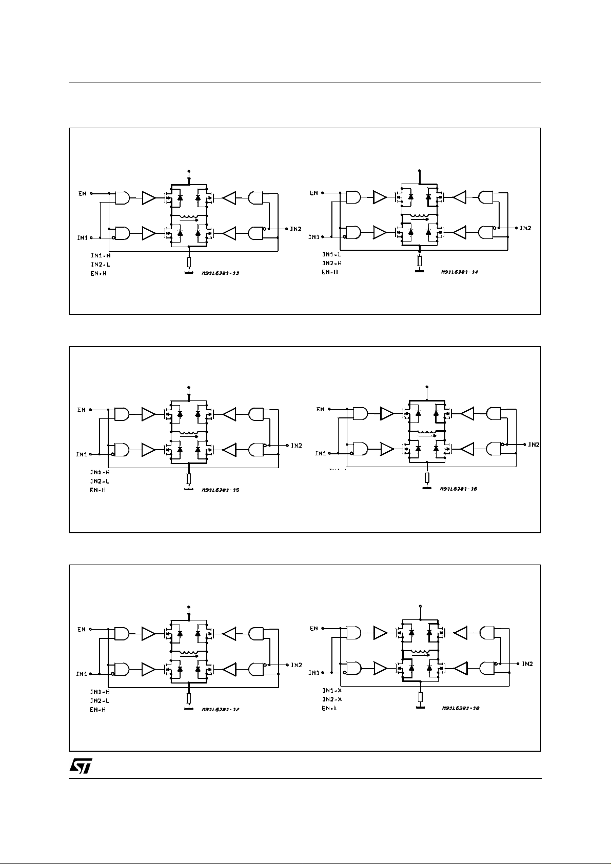
L6201 - L6202 - L6203
Figure 8a:
Figure 8b:
Two Phase Chopping
One Phase Chopping
Figure 8c:
IN1 = H
IN 2 = H
EN = H
Enable Chopping
7/20
 Loading...