

Page 1

L6201
L6202 - L6203
DMOS FULL BRIDGE DRIVER
SUPPLY VOLTAGE UP TO 48V
5A MAX PEAK CU RRENT (2A max. for L6201)
TOTAL RMS CURRENT UP TO
L6201: 1A; L6202: 1.5A; L6203/L6201PS: 4A
R
0.3 Ω (typical value at 25 °C)
DS (ON)
CROSS CONDUCTION PRO TECTION
TTL COMPATIBLE DRIVE
OPERATING FREQUENCY UP TO 100 KHz
THERMAL SHUTDOWN
INTERNAL LOGIC SUPPLY
HIGH EFFICIENCY
DESCRIPTION
The I.C. is a full bridge driver for motor control applications realized in Multipower-BCD technology
which combines isolated DMOS power transistors
with CMOS and Bipolar circuits on the same chip.
By using mixed technology it has been possible to
optimize the logic circuitry and the power stage to
achieve the best possible performance. The
DMOS output transistors can operate at supply
voltages up to 42V and efficiently at high switch-
BLOCK DIAGRAM
MULTIPOWER BCD TECHNOLOGY
Powerdip 12+3+3
Multiwatt11
ORDERING NUMBERS:
L6201
L6201PS
L6202
L6203
SO20 (12+4+4)
PowerSO20
(SO20)
(PowerSO20)
(Powerdip18)
(Multiwatt)
ing speeds. All the logic inputs are TTL, CMOS
and µC compatible. Each channel (half-bridge) of
the device is controlled by a separate logic input,
while a common enable controls both channels.
The I.C. is mounted in three different packages.
July 1997
This is advanced information on a new product now in development or undergoing evaluation. Details are subject to change without notice.
1/20
Page 2

L6201 - L6202 - L6203
PIN CONNECTIONS
(Top view)
SO20
GND
N.C.
N.C.
OUT2
OUT1
BOOT1
N.C.
GND 10
V
IN1
POWERDIP
1
2
3
4
S
5
6
7
8
9
D95IN216
20
19
18
17
16
15
14
13
12
11
GND
N.C.
N.C.
ENABLE
SENSE
Vref
BOOT2
IN2
N.C.
GND
2/20
PowerSO20
MULTIWATT11
Page 3

PINS FUNCTIONS
L6201 - L6202 - L6203
Device
L6201 L6201PS L6202 L6203
1 16 1 10 SENSE A resistor R
Name Function
connected to this pin provides feedback for
sense
motor current control.
2 17 2 11 ENABLEWhen a logic high is present on this pin the DMOS POWER
transistors are enabled to be selectively driven by IN1 and IN2.
3 2,3,9,12,
3 N.C. Not Connected
18,19
4,5 – 4
– 1, 10 5 GND Common Ground Terminal
GND Common Ground Terminal
6
6,7 – 6 GND Common Ground Terminal
8 – 7 N.C. Not Connected
9 4 8 1 OUT2 Ouput of 2nd Half Bridge
10 5 9 2 V
s
Supply Voltage
11 6 10 3 OUT1 Output of first Half Bridge
12 7 11 4 BOOT1 A boostrap capacitor connected to this pin ensures efficient
driving of the upper POWER DMOS transistor.
13 8 12 5 IN1 Digital Input from the Motor Controller
14,15 – 13
– 11, 20 14 GND Common Ground Terminal
GND Common Ground Terminal
6
16,17 – 15 GND Common Ground Terminal
18 13 16 7 IN2 Digital Input from the Motor Controller
19 14 17 8 BOOT2 A boostrap capacitor connected to this pin ensures efficient
driving of the upper POWER DMOS transistor.
20 15 18 9 V
ref
Internal voltage reference. A capacitor from this pin to GND is
recommended. The internal Ref. Voltage can source out a
current of 2mA max.
ABSOLUTE MAXIMUM RATINGS
Symbol Parameter Value Unit
V
V
IN
V
P
T
stg
Note 1:
Note 2:
V
OD
, V
I
sense
V
Power Supply 52 V
s
Differential Output Voltage (between Out1 and Out2) 60 V
Input or Enable Voltage – 0.3 to + 7 V
EN
Pulsed Output Current for L6201PS/L6202/L6203 (Note 1)
o
– Non Repetitive (< 1 ms) for L6201
for L6201PS/L6202/L6203
DC Output Current for L6201 (Note 1)
5
5
10
1
Sensing Voltage – 1 to + 4 V
Boostrap Peak Voltage 60 V
b
Total Power Dissipation:
tot
= 90°C for L6201
T
pins
for L6202
= 90°C for L6201PS/L6203
T
case
= 70°C for L6201 (Note 2)
T
amb
for L6202 (Note 2)
for L6201PS/L6203 (Note 2)
4
5
20
0.9
1.3
2.3
, TjStorage and Junction Temperature – 40 to + 150 °C
Pulse width limited only by junction temperature and transient thermal impedance (see thermal characteristics)
Mounted on board with minimized dissipating copper area.
A
A
A
A
W
W
W
W
W
W
3/20
Page 4

L6201 - L6202 - L6203
THERMAL DATA
Symbol Parameter
Rt
h j-pins
Rt
h j-case
Rt
h j-amb
(*) Mounted on aluminium substrate.
Thermal Resistance Junction-pins max
Thermal Resistance Junction Case max.
Thermal Resistance Junction-ambient max.
ELECTRICAL CHARACTERISTICS
L6201 L6201PS L6202 L6203
15
–
85
(Refer to the Test Circuits; T
Value
–
–
13 (*)
= 25°C, VS = 42V, V
j
12
–
60
–
3
35
= 0, unless
sens
otherwise specified).
Symbol Parameter Test Conditions Min. Typ. Max. Unit
V
s
V
ref
I
REF
I
s
f
c
T
j
T
d
Supply Voltage 12 36 48 V
Reference Voltage I
= 2mA 13.5 V
REF
Output Current 2mA
Quiescent Supply Current EN = H VIN = L
EN = H V
EN = L ( Fig. 1,2,3)
= H
IN
IL = 0
10
10
8
15
15
15
Commutation Frequency (*) 30 100 KHz
Thermal Shutdown 150 °C
Dead Time Protection 100 ns
TRANSISTORS
OFF
I
DSS
Leakage Current Fig. 11 Vs = 52 V 1 mA
ON
R
V
DS(ON)
V
DS
sens
On Resistance Fig. 4,5 0.3 0.55 Ω
Drain Source Voltage Fig. 9
I
DS
I
DS
I
DS
= 1A
= 1.2A
= 3A
L6201
L6202
L6201PS/0
3
0.3
0.36
0.9
Sensing Voltage – 1 4 V
SOURCE DRAIN DIODE
Unit
°C/W
mA
mA
mA
V
V
V
V
sd
t
rr
t
fr
Forward ON Voltage Fig. 6a and b
Reverse Recovery Time
Forward Recovery Time 200 ns
LOGIC LEVELS
V
V
I
4/20
IN L
IN H
I
IN L
IN H
, V
, V
, I
, I
Input Low Voltage – 0.3 0.8 V
EN L
Input High Voltage 2 7 V
EN H
Input Low Current VIN, VEN = L –10 µA
EN L
Input High Current VIN, VEN = H 30 µA
EN H
= 1A
I
SD
= 1.2A
I
SD
= 3A
I
SD
L
dif
= 25 A/µs
dt
I
= 1A
F
= 1.2A
I
F
= 3A
I
F
L6201
EN = L
L6202
EN = L
L6201PS/03
EN =
L6201
L6202
L6203
0.9 (**)
0.9 (**)
1.35(**)
300 ns
V
V
V
Page 5

L6201 - L6202 - L6203
ELECTRICAL CHARACTERISTICS
(Continued)
LOGIC CONTROL TO POWER DRIVE TIMING
Symbol Parameter Test Conditions Min. Typ. Max. Unit
t
(Vi) Source Current Turn-off Delay Fig. 12 300 ns
1
t
(Vi) Source Current Fall Time Fig. 12 200 ns
2
t
(Vi) Source Current Turn-on Delay Fig. 12 400 ns
3
t
(Vi) Source Current Rise Time Fig. 12 200 ns
4
t
(Vi) Sink Current Turn-off Delay Fig. 13 300 ns
5
t
(Vi) Sink Current Fall Time Fig. 13 200 ns
6
t
(Vi) Sink Current Turn-on Delay Fig. 13 400 ns
7
t
(Vi) Sink Current Rise Time Fig. 13 200 ns
8
(*)
Limited by power dissipation
(**)
In synchronous rectification the drain-source voltage drop VDS is shown in fig. 4 (L6202/03); typical value for the L6201 is of 0.3V .
Figure 1:
Typical Normalized I
vs. T
S
j
Figure 2:
Typical Normalized Quiescent Current
vs. Frequency
Figure 3:
Typical Normalized I
vs. V
S
S
Figure 4:
Typical R
DS (ON)
vs. VS ~ V
ref
5/20
Page 6

L6201 - L6202 - L6203
Figure 5:
Figure 6a:
Normalized R
at 25°C vs. Temperature Typical Values
DS (ON)
Typical Diode Behaviour in Synchro-
nous Rectification (L6201)
Figure 6b:
Typical Diode Behaviour in Synchro-
nous Rectification (L6201PS/02/03)
Figure 7a:
6/20
Typical Power Dissipation vs I
(L6201)
L
Figure 7b:
Typical Power Dissipation vs I
L
(L6201PS, L6202, L6203))
Page 7

L6201 - L6202 - L6203
Figure 8a:
Figure 8b:
Two Phase Chopping
One Phase Chopping
Figure 8c:
IN1 = H
IN 2 = H
EN = H
Enable Chopping
7/20
Page 8

L6201 - L6202 - L6203
TEST CIRCUITS
Figure 9:
Saturation Voltage
Figure 10:
Figure 11:
Quiescent Current
Leakage Current
8/20
Page 9

Figure 12: Source Current Delay Times vs. Input Chopper
42V for L6201PS/02/03
L6201 - L6202 - L6203
Figure 13: Sink Current Delay Times vs. Input Chopper
42V for L6201PS/02/03
9/20
Page 10

L6201 - L6202 - L6203
CIRCUIT DESCRIPTION
The L6201/1PS/2/3 is a monolithic full bridge
switching motor driver realized in the new Multipower-BCD technology which allows the integration of multiple, isolated DMOS power transistors
plus mixed CMOS/bipolar control circuits. In this
way it has been possible to make all the control
inputs TTL, CMOS and µC compatible and eliminate the necessity of external MOS drive components. The Logic Drive is shown in table 1.
Table 1
Inputs
IN1 IN2
L
V
= H
EN
= L X X All transistors turned oFF
V
EN
L = Low H = High X = DON’t care
(*) Numbers referred to INPUT1 or INPUT2 controlled output stages
L
H
H
L
H
L
H
Output Mosfets (*)
Sink 1, Sink 2
Sink 1, Source 2
Source 1, Sink 2
Source 1, Source 2
Although the device guarantees the absence of
cross-conduction, the presence of the intrinsic diodes in the POWER DMOS structure causes the
generation of current spikes on the sensing terminals. This is due to charge-discharge phenomena
in the capacitors C1 & C2 associated with the
drain source junctions (fig. 14). When the output
switches from high to low, a current spike is generated associated with the capacitor C1. On the
low-to-high transition a spike of the same polarity
is generated by C2, preceded by a spike of the
opposite polarity due t o the charging of the input
capacity of the lower POWER DMOS transistor
(fig. 15).
Figure 14: Intrinsic Structures in the POWER
DMOS Transistors
Figure 15: Current Typical Spikes on the Sens-
ing Pin
TRANSISTOR OPERATION
ON State
When one of the POWER DMOS transistor is ON
it can be considered as a resistor R
DS (ON)
throughout the recommended operating range. In
this condition the dissipated power is given by :
⋅ I
DS
2
(RMS)
The low R
P
= R
ON
DS (ON)
DS (ON)
of the Multipower-BCD process
can provide high currents with low power dissipation.
OFF State
When one of the POWER DMOS transistor is
OFF the V
age and only the leakage current I
voltage is equal to the supply volt-
DS
flows. The
DSS
power dissipation during this period is given by :
= VS ⋅ I
P
OFF
DSS
The power dissipation is very low and is negligible
in comparison to that dissipated in the ON
STATE.
10/20
Transitions
As already seen above the transistors have an intrinsic diode between their source a nd drain that
can operate as a fast freewheeling diode in
switched mode applications. During recirculation
with the ENABLE input high, the voltage drop
across the transistor is R
⋅ ID and when it
DS (ON)
reaches the diode forward voltage it is clamped.
When the ENABLE input is low, the POWER
MOS is OFF and the diode carries all of the recirculation current. The power dissipated in the transitional times in t he cycle depends upon the voltage-current waveforms and in the driving mode.
(see Fig. 7ab and Fig. 8abc).
= IDS (t) ⋅ VDS (t)
P
trans.
Page 11

L6201 - L6202 - L6203
Boostrap Capacitors
To ensure that the POWER DMOS transistors are
driven correctly gate to source voltage of typ. 10
V must be guaranteed for all of the N-channel
DMOS transistors. This is easy to be provided for
the lower POWER DMOS transistors as their
sources are refered to ground but a gate voltage
greater than the supply voltage is necessary to
drive the upper transistors. Th is is achieved by an
internal charge pump circuit that guarantees correct DC drive in combination with the boostrap circuit. For eff icient charging the value of the boostrap capacitor should be greater than the input
capacitance of the power transistor which is
around 1 nF. It is recommended that a capacitance of at least 10 nF is used for the bootstrap. If
a smaller capacitor is used there is a risk that the
POWER transistors will not be fully turned on and
they will show a higher RDS (ON). On the other
hand if a elev ated value is u sed it is possible that
a current spike may be produced in t he sense resistor.
Reference Voltage
To by-pass the internal Ref. Volt. circuit it is recommended that a capacitor be placed between its
pin and ground. A value of 0.22 µF should be sufficient for most applications. This pin is also protected against a short circuit to ground: a max.
current of 2mA max. can be sinked out.
Dead Time
To protect the device against simultaneous conduction in both arms of the bridge resulting in a
rail to rail short circuit, the integrated logic control
provides a dead time greater than 40 ns.
Thermal Protection
A thermal protection circuit has been included
that will disable the device if the junction temperature reaches 150 °C. When the temperature has
fallen to a safe level the device restarts the input
and enable signals under control.
APPLICATION INFORMATION
Recirculation
During recirculation with the ENABLE input high,
the voltage drop across the transistor is RDS
(ON)⋅ IL, clamped at a voltage depending on the
characteristics of the source-drain diode. Although the device is protected against cross conduction, current spikes can appear on the current
sense pin due to charge/discharge phenomena in
the intrinsic source drain capacitances. In the application this does not cause any problem because the voltage spike generated on the sense
resistor is masked by the current controller circuit.
Rise Time T
(See Fig. 16)
r
When a diagonal of the bridge is t urned on current begins to flow in the inductive load until the
maximum current I
The dissipated energy E
E
OFF/ON
Load Time T
LD
is reached after a time Tr.
= [R
L
DS (ON)
is in this case :
OFF/ON
2
⋅ I
L
⋅ T
] ⋅ 2/3
r
(See Fig.16)
During this time the energy dissipated is due to
the ON resistance of the transistors (E
to commutation (E
DMOS transistors are ON, E
E
= I
LD
). As two of the POWER
COM
2
L
⋅ R
DS (ON)
is given by :
ON
⋅ 2 ⋅ T
LD
LD
) and due
In the commutation the energy dissipated is :
E
COM
= V
⋅ IL ⋅ T
S
COM
⋅ f
SWITCH
⋅ T
LD
Where :
T
= T
COM
f
SWITCH
TURN-ON
= Chopping frequency.
Fall Time T
= T
TURN-OFF
(See Fig. 16)
f
It is assumed that the energy dissipated in this
part of the cycle takes the same form as that
shown for the rise time :
2
E
ON/OFF
= [R
DS (ON)
⋅ I
L
⋅ Tf] ⋅ 2/3
Figure 16.
11/20
Page 12

L6201 - L6202 - L6203
Quiescent Energy
The last contribution to the energy dissipation is
due to the quiesce n t s u pply c ur r e nt and is g iven b y :
E
QUIESCENT
= I
QUIESCENT
⋅ Vs ⋅ T
Total Energy Per Cycle
E
= E
TOT
+ E
ON/OFF
The Total Power Dissipation P
= Rise time
T
r
T
= Load drive time
LD
T
= Fall time
f
= Dead time
T
d
OFF/ON
P
= E
DIS
+ ELD + E
+ E
QUIE SC EN T
/T
TOT
COM
is simply :
DIS
+
T = Period
T = T
+ TLD + Tf + T
r
d
DC Motor Speed Control
Since the I.C. integrates a full H-Bridge in a single
package it is idealy suit ed for controlling DC motors. When used for DC motor control it performs
the power stage required for both speed and direction control. The device can be combined with
a current regulator like the L6506 to implement a
transconductance amplifier for speed control, as
shown in figure 17. In this particular configuration
only half of the L6506 is used and the other half
of the device may be used to control a second
motor.
The L6506 senses the voltage across the sense
resistor R
to monitor the motor current: it com-
S
pares the sensed voltage both to control the
speed and during the brake of the motor.
Between the sense resistor and each sense input
of the L6506 a resistor is recommended; if the
connections between the outputs of the L6506
and the inputs of the L6203 need a long path, a
resistor must be added between each input of the
L6203 and ground.
A snubber network made by the series of R and C
must be foreseen very near to the output pins of
the I.C.; one diode (BYW98) is connected between each power output pin and ground as well.
The following formulas can be used to calculate
the snubber values:
R ≅ V
S/lp
C = lp/(dV/dt) where:
V
is the maximum Supply Voltage foreseen on
S
the application;
is the peak of the load current;
I
p
dv/dt is the limited rise time of the output voltage
(200V/µs is generally used).
If the Power Supply Cannot Sink Current, a suitable large capacitor must be used and connected
near the supply pin of the L6203. Sometimes a
capacitor at pin 17 of the L6506 let the application
better work. For motor current up to 2A max., the
L6202 can be used in a similar circuit configuration for which a typical Supply Voltage of 24V is
recommended.
Figure 17: Bidirectional DC Motor Control
12/20
Page 13

L6201 - L6202 - L6203
BIPOLAR STEPPER MOTORS APPLICATIONS
Bipolar stepper motors can be driven with one
L6506 or L297, two full bridge BCD drivers and
very few external components. Together these
three chips form a complete microprocessor-tostepper motor interface is realized.
As shown in Fig. 18 and Fig. 19, the controller
connect directly to the two bridge BCD drivers.
External component are minimalized: an R.C. network to set the chopper frequency, a resistive divider (R1; R2) to establish the comparator reference voltage and a snubber network made by R
and C in series (See DC Motor Speed Control).
Figure 18: Two Phase Bipolar Stepper Motor Control Circuit with Chopper Current Control
L6201
L6201PS
L6202
L6203
L6201
L6201PS
L6202
L6203
Figure 19: Two Phase Bipolar Stepper M otor Control Circuit with Chopper Curr ent Control and T ranslator
L6201
L6201PS
L6202
L6203
L6201
L6201PS
L6202
L6203
13/20
Page 14

L6201 - L6202 - L6203
It could be requested to drive a motor at VS lower
than the minimum recommended one of 12V
(See Electrical Characteristics); in this case, by
accepting a possible small inc reas in t he R
DS (ON)
resistance of the power output transistors at the
lowest Supply Voltage value, may be a good solution the one shown in Fig. 20.
Figure 20: L6201/1P/2/3 Used at a Supply Volt-
age Range Between 9 and 18V
L6201
L6201PS
L6202
L6203
Figure 21: Typical R
Th J-amb
vs. "On Board"
Heatsink Area (L6201)
Figure 22: Typical Transient R
Condition (L6201)
in Single Pulse
TH
THERMAL CHARACTERISTICS
Thanks to the high ef ficiency of this device, oft en
a true heatsink is not needed or it is simply obtained by means of a copper side on the P.C.B.
(L6201/2).
Under heavy conditions, the L6203 needs a suitable cooling.
By using two square copper sides in a similar way
as it shown in Fig. 23, Fig. 21 indicates how to
choose the on board heatsink area when the
L6201 total power dissipation is known since:
R
Th j-amb
= (T
j max.
– T
amb max
) / P
tot
Figure 22 shows the Transient Thermal Resistance vs. a single pulse time width.
Figure 23 and 24 refer to the L6202.
For the Multiwatt L6203 addition information is
given by Figure 25 (Thermal Resistance JunctionAmbient vs. Total Power Dissipation) and Figure
26 (Peak Transient Thermal Resistance vs. Repetitive Pulse Width) while Figure 27 refers to the
single pulse Transient Thermal Resistance.
Figurre 23: Typical R
Square Heatsink (L6202)
Th J-amb
vs. Two "On Board"
14/20
Page 15

L6201 - L6202 - L6203
Figure 24: Typical Transient Thermal Resistance
for Single Pulses (L6202)
Figure 26: Typical Transient Thermal Resistance
for Single Pulses with and without
Heatsink (L6203)
Figure 25: Typical R
Th J-amb
of Multiwatt
Package vs. Total Power Dissipation
Figure 27: Typical Transient Thermal Resistance
versus Pulse Width and Duty Cycle
(L6203)
15/20
Page 16

L6201 - L6202 - L6203
POWERDIP18 PACKAGE MECHA NICAL DATA
DIM.
MIN. TYP. MAX. MIN. TYP. MAX.
a1 0.51 0.020
B 0.85 1.40 0.033 0.055
b 0.50 0.020
b1 0.38 0.50 0.015 0.020
D 24.80 0.976
E 8.80 0.346
e 2.54 0.100
e3 20.32 0.800
F 7.10 0.280
I 5.10 0.201
L 3.30 0.130
Z 2.54 0.100
mm inch
16/20
Page 17

SO20 PACKAGE MECHANICAL DATA
L6201 - L6202 - L6203
DIM.
MIN. TYP. MAX. MIN. TYP. MAX.
A 2.65 0.104
a1 0.1 0.3 0.004 0.012
a2 2.45 0.096
b 0.35 0.49 0.014 0.019
b1 0.23 0.32 0.009 0.013
C 0.5 0.020
c1 45 (typ.)
D 12.6 13.0 0.496 0.512
E 10 10.65 0.394 0.419
e 1.27 0.050
e3 11.43 0.450
F 7.4 7.6 0.291 0.299
L 0.5 1.27 0.020 0.050
M 0.75 0.030
S 8 (max.)
mm inch
17/20
Page 18
L6201 - L6202 - L6203
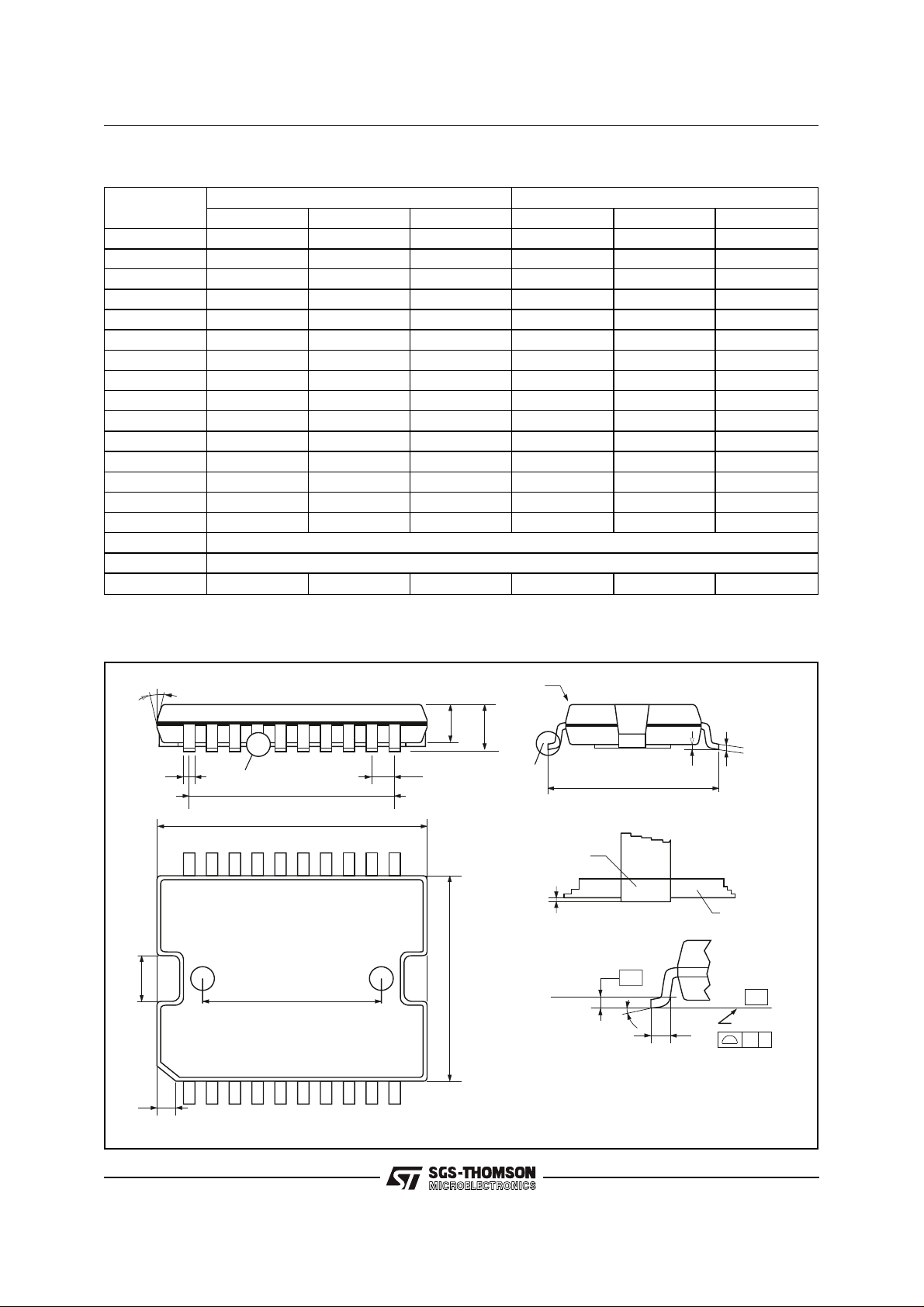
PowerSO20 PACKAGE MECHANICAL DATA
DIM.
MIN. TYP. MAX. MIN. TYP. MAX.
mm inch
A 3.60 0.1417
a1 0.10 0.30 0.0039 0.0118
a2 3.30 0.1299
a3 0 0.10 0 0.0039
b 0.40 0.53 0.0157 0.0209
c 0.23 0.32 0.009 0.0126
D (1) 15.80 16.00 0.6220 0.6299
E 13.90 14.50 0.5472 0.570
e 1.27 0.050
e3 11.43 0.450
E1 (1) 10.90 11.10 0.4291 0.437
E2 2.90 0.1141
G 0 0.10 0 0.0039
h 1.10
L 0.80 1.10 0.0314 0.0433
N10
S8
(max.)
°
(max.)
°
T 10.0 0.3937
(1) "D and E1" do not include mold flash or protrusions
- Mold flash or protrusions shall not exceed 0.15mm (0.006")
E2
h x 45°
NN
a2
A
b
DETAILA
e3
e
R
DETAILB
D
1120
E1
T
110
PSO20MEC
lead
a3
Gage Plane
E
DETAILB
0.35
S
a1
L
c
DETAILA
slug
-C-
SEATING PLANE
GC
(COPLANARITY)
18/20
Page 19

MULTIWATT11 PACKAGE MECHANICAL DATA
L6201 - L6202 - L6203
DIM.
A 5 0.197
B 2.65 0.104
C 1.6 0.063
D 1 0.039
E 0.49 0.55 0.019 0.022
F 0.88 0.95 0.035 0.037
G 1.57 1.7 1.83 0.062 0.067 0.072
G1 16.87 17 17.13 0.664 0.669 0.674
H1 19.6 0.772
H2 20.2 0.795
L 21.5 22.3 0.846 0.878
L1 21.4 22.2 0.843 0.874
L2 17.4 18.1 0.685 0.713
L3 17.25 17.5 17.75 0.679 0.689 0.699
L4 10.3 10.7 10.9 0.406 0.421 0.429
L7 2.65 2.9 0.104 0.114
M 4.1 4.3 4.5 0.161 0.169 0.177
M1 4.88 5.08 5.3 0.192 0.200 0.209
S 1.9 2.6 0.075 0.102
S1 1.9 2.6 0.075 0.102
Dia1 3.65 3.85 0.144 0.152
MIN. TYP. MAX. MIN. TYP. MAX.
mm inch
19/20
Page 20

L6201 - L6202 - L6203
Information furnis hed is believe d to be ac curate and reliabl e. However, SGS-THOMS ON Mi croelectroni cs as sumes no res ponsib ility for the
consequences of use of such information nor for any i nfringem ent of patents or othe r ri ghts of third parties whi ch may result from its use. No
license is granted by implication or otherwise under any patent or patent rights of SGS-THOMSON Microelectronics. Specification mentioned
in this p ublication are subject to c hange w ithout not ice. T his pub lic ation super sedes a nd replaces all informa tion previous ly supplied. SGSTHOMSON Mic roelectronics products are not author ized for use as cri tical components in l ife support devices or systems with out express
written approval of SGS-THOMSON Microelectronics.
© 1997 SGS-THOMSON Microelectronics – Printed in Italy – All Rights Reserved
SGS-THOMSON Microelectronics GROUP OF COMPANIES
Australia - Brazil - Canada - China - France - Germany - Hong Kong - Italy - Japan - Korea - Malaysia - Malta - Morocco - The Netherlands -
Singapore - Spain - Sweden - Switzerland - Taiwan - Thailand - United Kingdom - U.S.A.
20/20
Page 21

This datasheet has been download from:
www.datasheetcatalog.com
Datasheets for electronics components.
 Loading...