

STMicroelectronics L4975A User Manual
®
L4975A
5A SWITCHING REGULATOR
5A OUTPUT CURRENT
5.1V TO 40V OUTPUT VOLTAGE RANGE
0 TO 90% DUTY CYCLE RANGE
INTERNAL FEED-FORWARD LINE REGULA-
TION
INTERNAL CURRENT LIMITING
PRECISE 5.1V ± 2% ON CHIP REFERENCE
RESET AND POWER FAIL FUNCTIONS
SOFT START
INPUT/OUTPUT SYNC PIN
UNDER VOLTAGE LOCK OUT WITH HYS-
TERETIC TURN-ON
PWM LATCH FOR SINGLE PULSE PER PE-
RIOD
VERY HIGH EFFICIENCY
SWITCHING FREQUENCY UP TO 500KHz
THERMAL SHUTDOWN
CONTINUOUS MODE OPERATION
DESCRIPTION
The L4975A is a stepdown monolithic power
switching regulator delivering 5A at a voltage variable from 5.1 to 40V.
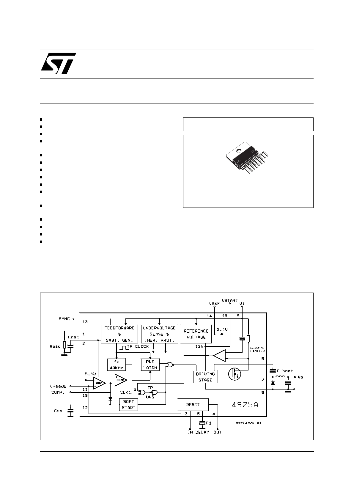
BLOCK DIAGRAM
MULTIPOWER BCD TECHNOLOGY
Multiwatt15V
ORDERING NUMBER:
Realized with BCD mixed technology, the device
uses a DMOS output transistor to obtain very high
efficiency and very fast switching times. F eatures
of the L4975A include reset and power fail for microprocessors, feed forward line regulation, soft
start, limiting current and thermal protection. The
device is mounted in a 15-lead multiwatt plastic
power package and requires few external components. Efficient operation at switching frequencies
up to 500KHz allows reduction in the size and
cost of external filter components.
L4975A
June 2000
This is advanced information on a new product now in development or undergoing evaluation. Details are subject to change without notice.
1/21
L4975A
ABSOLUTE MAXIMUM RATINGS
Symbol Parameter Value Unit
Input Voltage 55 V
Input Operating Voltage 50 V
Output DC Voltage
Output Peak Voltage at t = 0.1µs f = 200KHz
-1
-7
Maximum Output Current Internally Limited
Bootstrap Voltage
Bootstrap Operating Voltage
V
65
+ 15
9
Input Voltage at Pins 3, 12 12 V
Reset Output Voltage 50 V
Reset Output Sink Current 50 mA
Input Voltage at Pin 5, 10, 11, 13 7 V
Reset Delay Sink Current 30 mA
Error Amplifier Output Sink Current 1 A
Soft Start Sink Current 30 mA
Total Power Dissipation at T
< 120°C 30 W
case
Junction and Storage Temperature -40 to 150 °C
, V
V
5
V
9
V
9
V
7
I
7
V
6
, V
V
3
12
V
4
I
4
10, V11, V13
I
5
I
10
I
12
P
tot
, T
T
j
stg
V
V
V
V
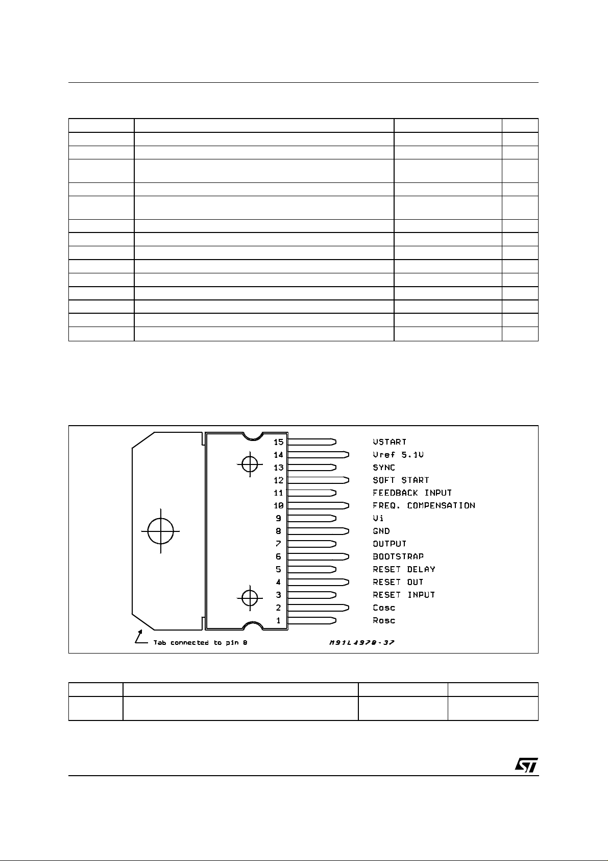
PIN CONNECTION
(Top view)
THERMAL DATA
Symbol Parameter Value Unit
R
th j-case
R
th j-amb
Thermal Resistance Junction-case max
Thermal Resistance Junction-ambient max
1
35
°C/W
°C/W
2/21
PIN FUNCTIONS
o
N
1 OSCILLATOR R
2 OSCILLATOR C
3 RESET INPUT Input of Power Fail Circuit. The threshold is 5.1V. It may be connected via a
4 RESET OUT Open Collector Reset/power Fail Signal Output. This output is high when the
5 RESET DELAY A C
6 BOOTSTRAP A C
7 OUTPUT Regulator Output.
8 GROUND Common Ground Terminal
9 SUPPLY VOLTAGE Unregulated Input Voltage.
10 FREQUENCY
COMPENSATION
11 FEEDBACK INPUT The Feedback Terminal of the Regulation Loop. The output is connected
12 SOFT START Soft Start Time Constant. A capacitor is connected between thi sterminal and
13 SYNC INPUT Multiple L4975A are synchronized by connecting pin 13 inputs together or via
14 V
15 V
Name Function
. External resistor connected to ground determines the constant charging
osc
ref
start
current of C
. External capacitor connected to ground determines (with R
osc
switching frequency.
divider to the input for power fail function. It must be connected to the pin 14 an
external 30KΩ resistor when power fail signal not required.
supply and the output voltages are safe.
capacitor connected between this terminal and ground determines the
d
reset signal delay time.
boot
drive properly the internal D-MOS transistor.
A series RC network connected between this terminal and ground determines
the regulation loop gain characteristics.
directly to this terminal for 5.1V operation; It is connected via a divider for higher
voltages.
ground to define the soft start time constant.
an external syncr. pulse.
5.1V V
Internal Start-up Circuit to Drive the Power Stage.
.
osc
capacitor connected between this terminal and the output allows to
Device Reference Voltage.
ref
osc
) the
L4975A
CIRCUIT OPERATION
(refer to the block dia-
gram)
The L4975 A is a 5A mono lith ic st ep down s witch ing
regulator working in continuous mode realized in
the new B CD Technology. Th is technology allows
the integration of isolated vertical DMOS power
transistors plus mixed CMOS/Bipolar transistors.
The device can deliver 5A at an output voltage
adjustable from 5.1V to 40V, and contains diagnostic and control functions that make it particularly suitable for microprocessor based systems.
BLOCK DIAGRAM
The block diagram shows the DMOS power transistor and the PWM control loop. Integrated functions include a reference voltage trimmed to 5.1V
±
2%, soft start, undervoltage lockout, oscillator
with feedforward control, pulse by pulse current
limit, thermal shutdown and finally the reset and
power fail circuit. The reset and power fail circuit
provides an output signal for a microprocessor indicating the status of the system.
Device turn on is around 11V with a typical 1V
hysteresis, this threshold provides a correct voltage for the driving stage of the DMOS gate and
the hysteresis prevents instabilities.
An external bootstrap capacitor charged to 12V
by an internal voltage reference is needed t o provide correct gate drive to t he power DMOS. The
driving circuit is able to source and sink peak currents of around 0.5A to the gate of the DMOS
transistor. A typical switching time of the current
in the DMOS transistor is 50ns. Due to the fast
commutation switching frequencies up to 500kHz
are possible.
The PWM control loop consists of a sawtooth oscillator, error amplifier, comparator, latch and the
output stage. An error signal is produced by comparing the output voltage with the precise 5.1V
2% on chip reference. This error signal is then
compared with the sawtooth oscillator, in order to
generate a fixed frequency pulse width modulated
drive for the output stage. A PWM latch is included to eliminate multiple pulsing within a period even in noisy environments. The gain and
3/21
±
L4975A
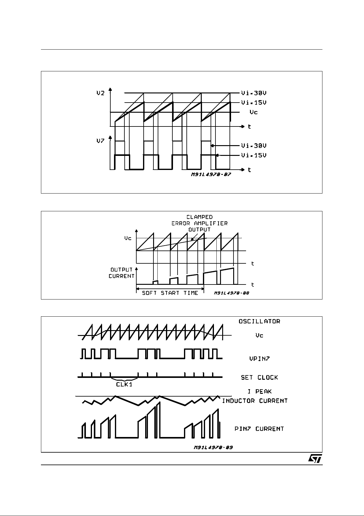
Figure 1:
Figure 2:
Feedforward Waveform
Soft Start Function
Figure 3:
4/21
Limiting Current Function
L4975A
stability of the loop can be adjusted by an external RC network connected to the output of the error amplifier. A voltage feedforward control has
been added to the oscillator, this maintains superior line regulation over a wide input voltage
range. Closing the loop directly gives an output
voltage of 5.1V, higher voltages are obtained by
inserting a voltage divider.
At turn on output overcurrents are prevented by
the soft start function (fig. 2). The error amplifier is
initially clamped by an external capacitor Css and
allowed to rise linearly under the charge of an internal constant current source.
Output overload protection is provided by a current limit circuit (fig. 3). The load current is sensed
by an internal metal resistor connected to a comparator. When the load current exceeds a preset
threshold the output of the comparator sets a flip
flop which turns off the power DMOS. The next
clock pulse, from an internal 40kHz oscillator will
reset the flip flop and the power DMOS will again
conduct. This current protection method, ensures
Figure 4:
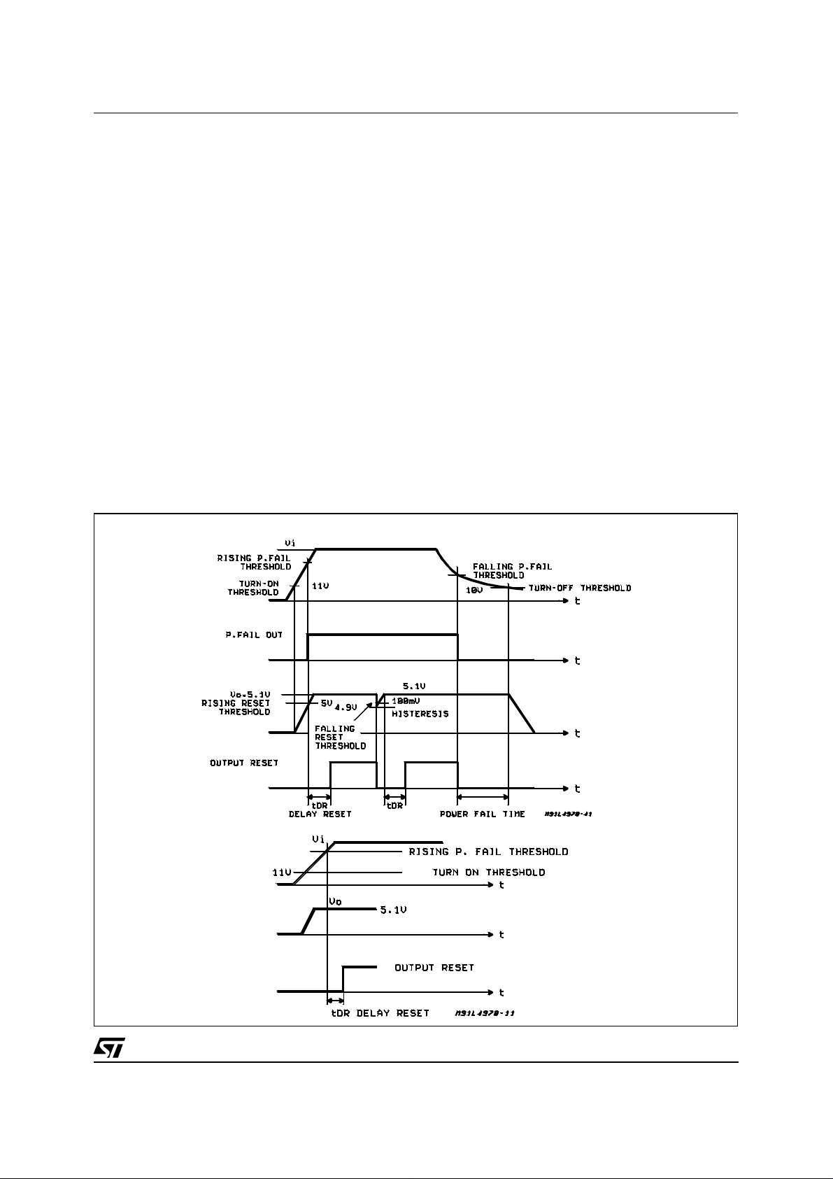
Reset and Power Fail Functions.
a constant current output when the system is
overloaded or short circuited and limits the
switching frequency, in this condition, to 40kHz.
The Reset and Power fail circuitry (fig 4) generates an output signal when the supply voltage exceeds a threshold programmed by an external
voltage divider. The reset signal, is generated
with a delay time programmed by an external capacitor on the delay pin. When the supply voltage
falls below the threshold or the output voltage
goes below 5V the reset output goes low immediately. The reset output is an open collector-drain.
Fig 4A shows the case when the supply voltage is
higher than the threshold, but the output voltage
is not yet 5V.
Fig 4B shows the case when the output is 5.1V
but the supply voltage is not yet higher than the
fixed threshold.
The thermal protection disables circuit operation
when the junction temperature reaches about
150°C and has an hysterysis to prevent unstable
conditions.
A
B
5/21
L4975A
ELECTRICAL CHARACTERISTICS
= 2.2nF, fSW = 200KHz typ, unless otherwise specified)
C
9
(Refer to the test circuit, T
= 25°C, Vi = 35V, R4 = 16KΩ,
j
DYNAMIC CHARACTERISTICS
Symbol Parameter Test Condition Min. Typ. Max. Unit Fig.
V
input Voltage Range (pin 9) Vo = V
i
I
V
o
Output Votage Vi = 15V to 50V
I
∆V
Line Regulation Vi = 15V to 50V
o
I
∆V
Load Regulation Vo = V
o
Io = 2A to 4A
I
V
d
Dropout Voltage Between
Pin 9 and 7
I
7L
Max. Limiting Current Vi = 15 to 50V
Io = 3A
I
V
η Efficiency I
V
Vo = 12V
Io = 5A
V
Vo = 12V
SVR Supply Voltage Ripple
Reject.
V
f = 100Hz; V
f Switching Frequency 180 200 220 KHz 5
∆ f
∆ V
∆ f
T
f
max
V
SECTION (pin 14)
ref
Voltage Stability of
Swiching Frequency
i
Temperature Stability of
Swiching Frequency
j
Maximum Operating
Switching Frequency
Vi = 15V to 45V 2 6 % 5
Tj = 0 to 125°C1%5
Vo = V
I
to 40V
ref
= 5A
o
= 3A; Vo = Vref
o
= 2A; Vo = Vref
o
ref
= 1A to 5A
o
= 5A
o
= V
to 40V
o
ref
= 3A
o
= V
o
ref
= V
o
ref
= 2VRMS; Io = 3A
i
= 5A; C9 = 1nF
o
= V
o
; R4 = 10KΩ
ref
15 50 V 5
5 5.1 5.2 V 5
12 30 mV 5
10
20
0.4
0.55
30
50
0.6
0.8
mV
mV
V
V
5.5 6.5 7.5 A 5
70 75
80
80 85
92
%
%
%
%
56 60 dB 5
ref
500 KHz 5
5
5
5
5
Symbol Parameter Test Condition Min. Typ. Max. Unit Fig.
V
∆V
∆V
∆ V
∆T
14
Reference Voltage 5 5.1 5.2 V 7
Line Regulation Vi = 15V to 50V 10 25 mV 7
14
Load Regulation I14 = 0 to 1mA 20 40 mV 7
14
14
Average Temperature
Tj = 0°C to 125°C 0.4 mV/°C7
Coefficient Reference
Voltage
V
START
I
14 short
Short Circuit Current Limit V14 = 0 70 mA 7
SECTION (pin 15)
Symbol Parameter Test Condition Min. Typ. Max. Unit Fig.
V
∆V
∆V
I
15 short
15
Reference Voltage 11.4 12 12.6 V 7
Line Regulation Vi = 15 to 50V 0.6 1.4 V 7
15
Load Regulation I15 = 0 to 1mA 50 200 mV 7
15
Short Circuit Current Limit V15 = 0V 80 mA 7
6/21
L4975A
ELECTRICAL CHARACTERISTICS
(continued)
DC CHARACTERISTICS
Symbol Parameter Test Condition Min. Typ. Max. Unit Fig.
V
V
9on
9 Hyst
I
9Q
I
9OQ
I
7L
Turn-on Threshold 10 11 12 V 7A
Turn-off Hysteresys 1 V 7A
Quiescent Current V12 = 0; S1 = D 13 19 mA 7A
Operating Supply Current V12 = 0; S1 = C; S2 = B 16 23 mA 7A
Out Leak Current Vi = 55V; S3 = A; V12 = 0 2 mA 7A
SOFT START
Symbol Parameter Test Condition Min. Typ. Max. Unit Fig.
I
12
V12Output Saturation Voltage I12 = 20mA; V9 = 10V
Soft Start Source Current V12 = 3V; V11 = 0V 70 100 130 µA7B
I
= 200µA; V9 = 10V
12
1
0.7
V
V
ERROR AMPLIFIER
Symbol Parameter Test Condition Min. Typ. Max. Unit Fig.
V
10H
V
10L
I
10H
I
10L
I
11
G
V
High Level Out Voltage I10 = -100µA; S1 = C
V
= 4.7V
11
Low Level Out Voltage I10 = +100µA; S1 = C
V
= 5.3V;
11
Source Output Current V10 = 1V; S1 = E
V
= 4.7V
11
Sink Output Current V10 = 6V; S1 = D
V
= 5.3V
11
Input Bias Current RS = 10KΩ 0.4 3 µA–
DC Open Loop Gain V
VCM
R
S
= 10Ω
SVR Supply Voltage Rejection 15 < V
R
= 10Ω
S
V
OS
Input Offset Voltage RS = 50Ω 210mV–
= 4V;
< 50V;
i
6V7C
1.2 V 7C
100 150 µA7C
100 150 µA7C
60 dB –
60 80 dB –
RAMP GENERATOR (pin 2)
7B
7B
Symbol Parameter Test Condition Min. Typ. Max. Unit Fig.
V
2
V
2
I
2
I
2
Ramp Valley S1 = C; S2 = B 1.2 1.5 V 7A
Ramp Peak S1 = C Vi = 15V
S2 = B V
= 45V
i
2.5
5.5
V
V
Min. Ramp Current S1 = A; I1 = 100µA 270 300 µA7A
Max. Ramp Current S1 = A; I1 = 1mA 2.4 2.7 mA 7A
SYNC FUNCTION (pin 13)
Symbol Parameter Test Condition Min. Typ. Max. Unit Fig.
V
13
V
13
I
13L
I
13H
V
13
t
W
Low Input Voltage Vi = 15V to 50V; V12 = 0;
S1 = C; S2 = B; S4 = B
High Input voltage V
12
= 0;
S1 = C; S2 = B; S4 = B
Sync Input Current with
Low Input Voltage
Input Current with High
Input Voltage
V2 = V13 = 0.9V; S4 = A;
S1 = C; S2 = B
V13 = 3.5V; S4 = A;
S1 = C; S2 = B
Output Amplitude 4 5 V –
Output Pulse Width V
= 2.5V 0.3 0.5 0.8 µs–
thr
–0.3 0.9 V 7A
3.5 5.5 V 7A
0.4 mA 7A
2mA7A
7A
7A
7/21
 Loading...