

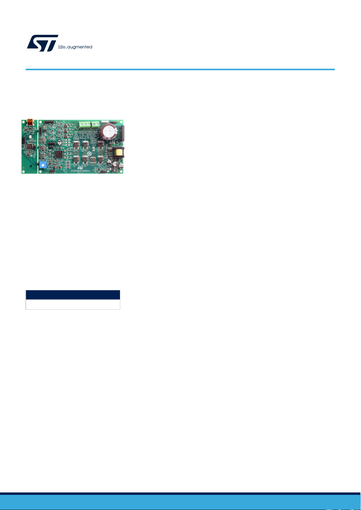
EVSPIN32F06Q2S1
3-phase inverter based on STSPIN32F0602
Features
• Input voltage from 35 VAC (50 VDC) to 280 VAC (400 VDC)
• STD18N65M5 MOS power stage featuring:
– V
– R
• Overcurrent threshold set to 8.5 A
• Dual footprint for IGBT/MOSFET package:
– DPAK
– PowerFlat 8x8 HV
• Single-shunt current sensing, suitable for:
– Sensored or sensorless 6-step algorithm
– Sensored or sensorless single-shunt vector (FOC) algorithm
• Smart shutdown overcurrent protection
• Digital Hall sensors and encoder input
• Bus voltage sensing
• 15 V VCC and 3.3 V VDD supplies
• Embedded ST-LINK/V2-1
• Easy user interface with buttons and trimmer
• RoHS compliant
@ T
(DS)
max. = 0.220 Ω
DS(on)
Jmax
= 710 V
peak
Data brief
Product status link
EVSPIN32F06Q2S1
Applications
• Home and Industrial refrigerators compressors
• Industrial drives, pumps, fans
• Air conditioning compressors & fans
• Corded power tools, garden tools
• Home appliances
• Industrial automation
Description
The EVSPIN32F06Q2S1 board is a 3-phase complete inverter based on the
STSPIN32F0602 controller, which embeds a 3‑phase 600 V gate driver and a
Cortex®-M0 STM32 MCU. The power stage features STD18N65M5 MOSFET, but
can be populated with any IGBT or Power MOSFET in DPAK or powerFLAT 8x8 HV
package.
The board has a single-shunt sensing topology, and both sensored and sensorless
FOC and 6-step control algorithms can be implemented. This allows driving
permanent magnet synchronous motors (PMSMs) and brushless DC (BLDC) motors.
The evaluation board is compatible with a wide range input voltage from 35 VAC
(50 VDC) to 280 VAC (400 VDC), and includes a power supply stage with the
VIPER06XS in flyback configuration to generate +15 V and +3.3 V supply voltage
required by the application.
DB4378 - Rev 1 - January 2021
For further information contact your local STMicroelectronics sales office.
www.st.com

EVSPIN32F06Q2S1
Debug and configuration of FW can be performed with standard STM32 tools through
the detachable ST-LINK‑debugger. SWD and UART TX‑RX connectors are also
available.
DB4378 - Rev 1
page 2/22
1 Safety and operating instructions
1.1 General terms
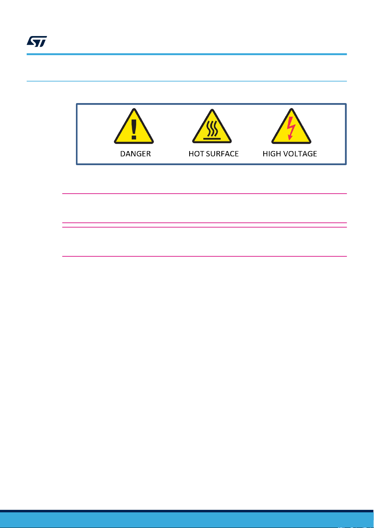
Warning:
During assembly, testing, and operation, the evaluation board poses several inherent hazards,
including bare wires, moving or rotating parts and hot surfaces.
EVSPIN32F06Q2S1
Safety and operating instructions
Danger:
There is danger of serious personal injury, property damage or death due to electrical shock and
burn hazards if the kit or components are improperly used or installed incorrectly.
The kit is not electrically isolated from the high-voltage supply AC/DC input. The evaluation board is
directly linked to the mains voltage. No insulation is ensured between the accessible parts and the high
voltage. All measuring equipment must be isolated from the mains before powering the board. When
using an oscilloscope with the demo, it must be isolated from the AC line. This prevents shock from
occurring as a result of touching any single point in the circuit, but does NOT prevent shock when
touching two or more points in the circuit.
All operations involving transportation, installation and use, and maintenance must be performed by skilled
technical personnel able to understand and implement national accident prevention regulations. For the purposes
of these basic safety instructions, “skilled technical personnel” are suitably qualified people who are familiar with
the installation, use and maintenance of power electronic systems.
1.2 Intended use of evaluation board
The evaluation board is designed for demonstration purposes only, and must not be used for electrical
installations or machinery. Technical data and information concerning the power supply conditions are detailed
in the documentation and should be strictly observed.
1.3 Installing the evaluation board
• The installation and cooling of the evaluation board must be in accordance with the specifications and target
application.
• The motor drive converters must be protected against excessive strain. In particular, components should not
be bent or isolating distances altered during transportation or handling.
• No contact must be made with other electronic components and contacts.
• The board contains electrostatically-sensitive components that are prone to damage if used incorrectly. Do
not mechanically damage or destroy the electrical components (potential health risks).
DB4378 - Rev 1
page 3/22

1.4 Operating the evaluation board
To operate properly the board, follow these safety rules.
1. Work Area Safety:
– The work area must be clean and tidy.
– Do not work alone when boards are energized.
– Protect against inadvertent access to the area where the board is energized using suitable barriers and
signs.
– A system architecture that supplies power to the evaluation board must be equipped with additional
control and protective devices in accordance with the applicable safety requirements (i.e., compliance
with technical equipment and accident prevention rules).
– Use non-conductive and stable work surface.
– Use adequately insulated clamps and wires to attach measurement probes and instruments.
2. Electrical Safety:
– Remove power supply from the board and electrical loads before performing any electrical
measurement.
– Proceed with the arrangement of measurement setup, wiring or configuration paying attention to high
voltage sections.
– Once the setup is complete, energize the board.
EVSPIN32F06Q2S1
Operating the evaluation board
Danger:
Do not touch the evaluation board when it is energized or immediately after it has been
disconnected from the voltage supply as several parts and power terminals containing potentially
energized capacitors need time to discharge.
Do not touch the boards after disconnection from the voltage supply as several parts like heat
sinks and transformers may still be very hot.
The kit is not electrically isolated from the AC/DC input. The USB interface of the board does not
insulate host computer from high voltage. When the board is supplied at a voltage outside the ELV
range, a proper insulation method such as a USB isolator must be used to operate the board.
3. Personal Safety
– Always wear suitable personal protective equipment such as, for example, insulating gloves and safety
glasses.
– Take adequate precautions and install the board in such a way to prevent accidental touch. Use
protective shields such as, for example, insulating box with interlocks if necessary.
DB4378 - Rev 1
page 4/22
2 Schematic diagrams
SPEED
OD
ZCR
SPI1_NSS/PROC
SPI1_MOSI/GPIO
SPI1_MISO/GPIO
SPI1_CLK/COMM
Boot from:
CLOSED 2-3 Flash
OUT3
OUT2
OUT1
GND
CLOSED 1-2 System/SRAM
PGND
CIN
VDD
VCC
VCC
VDD
VDD
VDDVDD
VDD
VDD
VDD
VCC
VCC
VCC
HV
HV
HV
HV
VDD VDD VDD
VCCVCC
VDD
HV
HV
HV
VDD
UART1_TX
UART1_RX
SWD_C LK
SWD_IO
GPIO_BE MF
PA0
PA1
PA2
PC14
PC15
NRST
OUT1
OUT2
OUT3
Temp_fdbk
VBUS_fdbk
R59 0R
R56
22R
C8
N.M.
Q6A
N.M.
1
2 3 4
5
TP20
TP4
TP8
Q9A
N.M.
1
2 3 4
5
TP19
1 2
TP5
U1
72
BOOT0
STSP IN32F0 602Q
BOOT1
40
47
BOOT2
53
BOOT3
CIN
27
EXP
EPAD
GND
28
HVG1
39
HVG2
46
HVG3
52
LVG1
30
LVG2
31
LVG3
32
NRST
10
OD
26
OUT1
38
OUT2
45
OUT3
51
PA0
13
PA1
14
PA12
63
PA1364PA14
65
PA15
66
PA2
15
PA3
16
PA4
17
PA5
19
PA620PA7
21
PB0
22
PB1
23
PB3
67
PB468PB569PB6
70
PB7
71
PB8
2
5
PC1 3
6
PC1 4
7
PC1 5
8
PF0
9
PF1
PGND
29
RES 1
60
RES 2
61
RES 3
62
RES 4
33
RES 5
VCC
58
1
RES 6
RES 7
18
59
4
VDD
VDD
24
VDDA
12
3
VSS
VSS
25
VSSA
11
C26
1uF/50 V
C13
N.M.
R49
4R7
TP14
C24
4.7uF/1 0V
R15
27R
TP16
TP18
C69
100nF /25V
D7
BAT54J
TP25
D4
BAT54J
D2
BAT54J
V+
+
V-
U3
TS302 1ILT
R13
22R
Q4
3
1
STD18 N65M5
2
TP17
C19
1
100nF /25V
2
C33
N.M.
R10
4R7
R16
4R7
J1
123
4
R57
100k
R58 0R
R42
22R
V-
V+
+
-
U2
TSV911 ILT
TP10
R52 10k
C9
33nF/6 30V
R27
4R7
R39
N.M.
R26
0R
TP6
Q6
3
1
STD18 N65M5
2
C30
100nF /25V
C16
4.7nF/2 5V
R14
100k
R2
4R7
D11
N.M.
D13
BAT54J
C31
4.7uF/1 0V
C23
100nF /25V
R111
N.M.
D6
N.M.
R36
0R1-2W-1 %
R18
22R
C10
10pF/5 0V
R1
27R
R23
100k
13
2
R29
0R
C27
33pF/2 5V
C4
N.M.
Q1A
N.M.
1
2 3 4
5
C18
47nF/2 5V
R44
100k
C11
10pF/5 0V
R35
27R
J9
123
4
Q4A
N.M.
1
2 3 4
5
R5
100k
C7
N.M.
R3
22R
C12
1uF/50 V
R55
3k
R32
47k
D9
BAT54J
X1
8MHz
R38 1k
TP23
R33
63.4k
JP1
1
3
CLOSED 2-3
2
Q9
3
1
STD18 N65M5
2
R60 33k
TP7
C1
100nF /25V
C3
1uF/50 V
0R
R109
C32 N.M.
C17
N.M.
C35
100nF /25V
C21
100nF /25V
Q3
3
1
STD18 N65M5
2
C2
220nF /25V
TP11
C22
1nF/25 V
TP22
Q7A
N.M.
1
2 3 4
5
D12
BAT54J
R30
22R
Q3A
N.M.
1
2 3 4
5
D1
N.M.
Q7
3
1
STD18 N65M5
2
TP1
Q1
3
1
STD18 N65M5
2
R31
100k
R61
10M
TP24
TP21
TP12
TP2
C67
47nF/2 5V
R19
100k
TP13
C20
100nF /25V
R34
0R1-2W-1 %
R40
4R7
R113
33k
R41
3k
TP3
C25
N.M.
CPOUT
CURRE NT_REF
SENS E_P
CURRE NT_REF
CPOUT
SENS E
LVG3
GH3
GL3
GH2
GL2
GL1
LVG1
GH1
LVG2
Curr_fdbk
LVG3
LVG2
LVG1
SENS E
SENS E
GH1
GL1
GH2
GL2
GH3
GL3
CIN
Curr_fdbk
SENS E_P
SENS E_N
SENS E_N
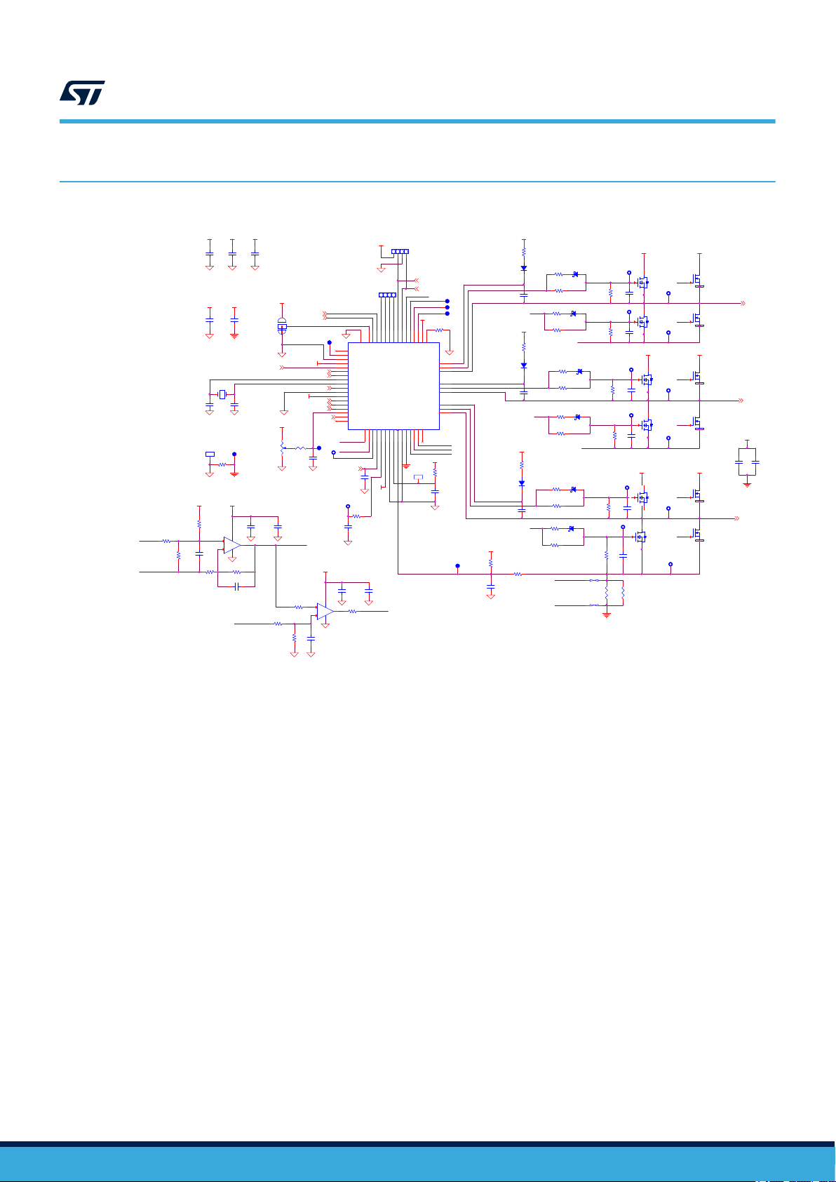
Figure 1. EVSPIN32F06Q2S1 schematic – Driver output stages
EVSPIN32F06Q2S1
Schematic diagrams
DB4378 - Rev 1
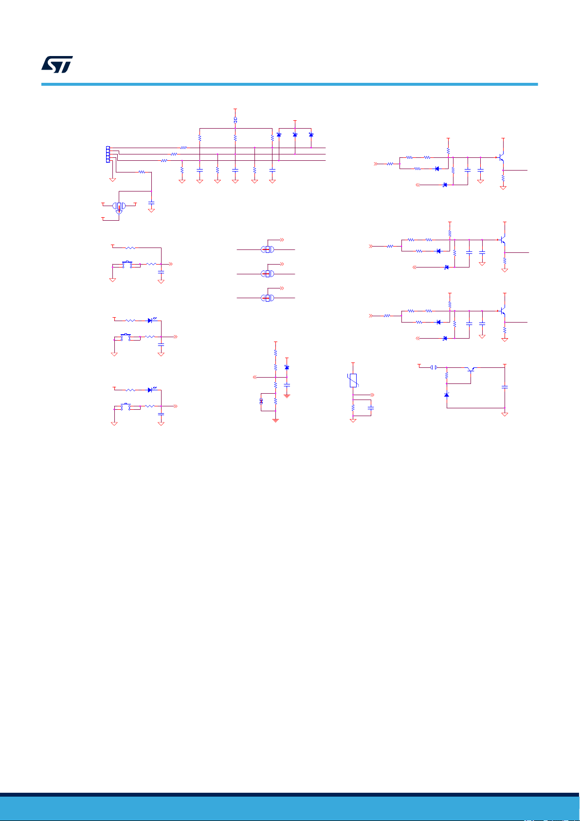
Figure 2. EVSPIN32F06Q2S1 schematic – Feedback network
page 5/22
RESET
USER1
USER2
10k
BEMF2
BEMF1
BEMF3 HALL
VDD
HALL PWR
Z+/H3
GND
A+/H1
B+/H2
5V
VDD
VCC
VDD
VDD
VDD
HV
VDD
VDD
VDD
VDD
VDD VDD
VDD VDD
VDD VDD
+5V
VCC
VCC
+5V
VDD
NRST
OUT3
OUT2
OUT1
PA0
PA1
PA2
VBUS_fdbk
Temp_fdbk
PC1 4
PC1 5
GPIO_BE MF
GPIO_BE MF
GPIO_BE MF
D8
STTH1L06 A
R51
2.7k
C68
4.7uF /50V
C36
1nF/25 V
J3
1
2
3
4
5
D5
BAT54J
R53
10k
R43
1M
Q2
2
1
3
R66
BC817 -25 or E quivalent
100R
R74
N.M.
C28
N.M.
R22
0R
C15
4.7pF/5 0V
R25
2.7k
JP 4
1 3
CLOSE D 1-2
2
C43
100n F/25V
R72
1
N.M.
2
SW3
13
4
4304 83025 816
2
R20
180k
R28
10k
R80
1k
SW1
13
4
4304 83025 816
2
D3
STTH1L06 A
R24
1k
R68 1.8k
R8
0R
R81
4.7k
Q8
2
1
3
R77
BC817 -25 or E quivalent
120R
R21
180k
C14
N.M.
D19
BAT54J
C39
10pF/1 0V
R17
1M
D18
BAT54J
C41
100n F/25V
C6
4.7pF/5 0V
SW2
13
4
4304 83025 816
2
C40
N.M.
1
JP 11
3
24
R54
100R
D10
BAT54J
R76
N.M.
R70 1.8k
R12
10k
JP 5
1 3
CLOSE D 1-2
2
D15
BAT54J
C38
10pF/1 0V
JP 6
CLOSE D
JP 10
OPE N
JP 3
1 3
2
CLOSE D 1-2
C5
N.M.
Q11
1
2
3STF 1640
3
D14
STTH1L06 A
LD2
YELLOW
R75
N.M.
Q5
2
1
3
R11
BC817 -25 or E quivalent
2.7k
JP 2
OPE N
R78
6.49k
R64
10k
D26
DDZ9690 T
R62
120R
R46
180k
R69
470k
R67
470k
R50
1k
R7
180k
C42
1nF/25 V
R63
10k
D17
BAT54J
R45
180k
R65
10k
R71 1.8k
R112
8k2
R47
0R
R73 0R
D16
BAT54J
R9
1k
R48
39k
R79
100R
R4
1M
C29
4.7pF/5 0V
LD1
YELLOW
R6
180k
C34
3.3NF/2 5V
C37
10pF/1 0V
PA0_BE MF PA0_Ha ll
PA1_BE MF PA1_Ha ll
PA2_BE MF PA2_Ha ll
Z+/H3_C
B+/H2_C
A+/H1_C
PA1_Ha ll
PA2_Ha ll
PA0_Ha ll
PA2_BE MF
PA1_BE MF
PA0_BE MF
EVSPIN32F06Q2S1
Schematic diagrams
DB4378 - Rev 1
page 6/22
Figure 3. EVSPIN32F06Q2S1 schematic – Power Supply
AC MAINS ~
Vcc_F
VCC
VDD
E3V3
GND
3V3_STLINK
OUT3
OUT2
OUT1
E3V3
HV
Vcc_F
HV
Vcc_F VCC
VDDE3V3
3V3_S TLINK
VDD
OUT1
OUT2
OUT3
R88
1.5k
1/4W
D21
3V3 N.M.
R82
330R
R110
220K 1/3 W
R83 0 R
-+
D20
2
GBU805
3
4 1
R85
10R
D24
BAT54J
C52
680n F/10V
R89
10k
J2
1
2
3
D25
12
STTH1L06 A
C51
820p F/25V
R87
22k
U4
2
Vout
LD1117S 33CTR
1
GND
3
Vin
J4
1
2
R86
22k
RV1
N.M.
+
C46
470u F/10V
+
C49
47uF /25V
U5
F1 10A/277 V slow
FB
4
VIPER0 6XS
3
LIM
8
DRAIN
1
GND
2
VDD
5
COMP
7
DRAIN6DRAIN
10
DRAIN9DRAIN
D23
12
STP S11 50A
LD3
RED
JP 7
1
2
3
CLOSE D 1-2
C47
100n F/25V
C44A
N.M.
C44
150u F/420V
C48
10uF /10V
LD4
GRE EN
+
C50
10uF /35V
NTC1
2R2
1 2
F1A N. M.
T1
3
4
2
1
5
8
C66
220p F/630V
R84
36k
+
C45
22uF /25V
D22
12
STP S05 60Z
JP 8
1
2
CLOSE D 1-2
3
EVSPIN32F06Q2S1
Schematic diagrams
DB4378 - Rev 1
page 7/22

TXRX
D-
D+
3V3_S TLINK
STRIP 1x4
STLINK FW LOAD
VDD
3V3_S TLINK
3V3_S TLINK
3V3_S TLINK
VUSB
3V3_S TLINK
VUSB
VUSB
VDD
3V3_S TLINK
UART1_TX
UART1_RX
SWD_IO
SWD_C LK
NRST
R102
100R
R107
100R
R94
4.7k
R108
100R
J5
6510 051612 1
1
USB_VCC
2
USBDM
3
USBDP
5
USB_GND
6
SHELL
7
SHELL
8
SHELL
ID
4
9
SHELL
C59
10pF /50V
R101 0R
C61
100n F/50V
R97 0R
R98
4.7k
C57
10nF /25V
R99 0R
U7
2
GND
LD3985M33R
OUT
5
1
VIN
4
BYPASS
3
INHIBIT
C62
100n F/25V
R104
N.M.
C53
100n F/25V
TP15
J8
1
CLOSE D
2
Q10
1
BC847 B
2 3
R100
4.7k
1
U6 USBLC6-2 SC6
I/O1#1
GND
2
5
VBUS
4
I/O2#4
6
I/O1#6
3
I/O2#3
J6
1
2
STRIP 1x2
R96
2.7k
C55
100n F/25V
JP 9
1
OP EN
2
C63
100n F/25V
R92
1.5k
C56
100n F/25V
X2
8MHz
C65
100n F/25V
R106
100k
R91
100R
C60
10pF /50V
J7
1
2
3
4
U8
PB7
43
STM32F 103CBT6
PB6
42
PB5
41
40
PB4/J NTRST
39
PB3/J TDO
10
PA0-WKUP
PA1
11
PA2
12
PA3
13
PA4
14
PA5
15
PA6
16
PA7
17
PA8
29
PA9
30
PA10
31
PA11
32
PA12
33
PA13
34
PB0
18
PB1
19
20
PB2/BO OT1
PB8
45
PB9
46
PB10
21
PB11
22
PB12
25
PB13
26
PB14
27
PB15
28
2
PC1 3-TAMPER -RTC
3
PC1 4-OSC3 2_IN
4
VSS_ 1
23
PC1 5-OSC3 2_OUT
5
OSC IN/PD0
7
NRST
6
OSC OUT/PD1
8
VSSA
35
VSS_ 2
47
VSS_ 3
1
VBAT
PA14
37
PA15
38
24
VDD_1
BOOT0
44
VDD_3
48
36
VDD_2
9
VDDA
C58
1uF/1 0V
R105
100k
C54
1uF/1 0V
R93
36k
LD5
K1
RED-GR EEN
A1
K2 A2
R103 1 0k
R90
10k
R95 0R
C64
100n F/25V
USB_DP
USB_DM
USB_R ENUM
SWDIO
STLINK_TX
STLINK_RX
T_NRS T
LED_STLINK
LED_STLINK
USB_DM USB_R ENUM
USB_DP
FM_SW CLK
FM_SW DIO
T_JTC K
T_JTC K
T_JTC K
T_JTMS
T_JTMS
T_NRS T
EVSPIN32F06Q2S1
Figure 4. EVSPIN32F06Q2S1 schematic – STLINK debugger
Schematic diagrams
DB4378 - Rev 1
page 8/22

EVSPIN32F06Q2S1
Bill of materials
3 Bill of materials
Table 1. EVSPIN32F06Q2S1 Bill of Materials
Components common to all device variants
Reference Part Value Description Package Manufacturer Part Number
C1, C19, C20,
C21, C23, C30,
C35, C41, C43,
C47, C53, C55,
C56, C62, C63,
C64, C65, C69
C2 220nF/25V SMT Ceramic Capacitor Size 0603
C3, C12, C26 1uF/50V SMT Ceramic Capacitor Size 0805
C4, C5, C7, C13,
C14, C17, C25,
C28, C32, C33,
C40
C6, C15, C29 4.7pF/50V SMT Ceramic Capacitor Size 0603
C8 N.M. Film, Metallized Polypropylene
C9 33nF/630V SMT Ceramic Capacitor Size 1210
C10, C11, C59,
C60
C16 4.7nF/25V SMT Ceramic Capacitor Size 0603
C18, C67 47nF/25V SMT Ceramic Capacitor Size 0603
C22, C36, C42 1nF/25V SMT Ceramic Capacitor Size 0603
C24, C31 4.7uF/10V SMT Ceramic Capacitor Size 0805
C27 33pF/25V SMT Ceramic Capacitor Size 0603
C34 3.3NF/25V SMT Ceramic Capacitor Size 0603
C37, C38, C39 10pF/10V SMT Ceramic Capacitor Size 0603
C44A N.M.
C44 150uF/420V
C45 22uF/25V SMD Aluminum Elect. Capacitor 5x5.4 mm
C46 470uF/10V SMD Aluminum Elect. Capacitor 6.3x7.7 mm Panasonic EEEFTA471XAP
C48 10uF/10V SMT Ceramic Capacitor Size 1206
C49 47uF/25V SMD Aluminum Elect. Capacitor 6.3x5.8 mm
100nF/25V SMT Ceramic Capacitor Size 0603
N.M. SMT Ceramic Capacitor Size 0603
4x13 mm,
Pitch 10 mm
10pF/50V SMT Ceramic Capacitor Size 0603
THT Electrolytic Capacitor, Radial
p7.5 d18h25
THT Electrolytic Capacitor, Radial
p10 d22h27 105C
Radial p7.5
d18h25 mm
Radial p10
d22h27.5 mm
WURTH
ELEKTRONIK
WURTH
ELEKTRONIK
WURTH
ELEKTRONIK
WURTH
ELEKTRONIK
KEMET R71MF31004030K
WURTH
ELEKTRONIK
WURTH
ELEKTRONIK
WURTH
ELEKTRONIK
WURTH
ELEKTRONIK
WURTH
ELEKTRONIK
WURTH
ELEKTRONIK
WURTH
ELEKTRONIK
WURTH
ELEKTRONIK
WURTH
ELEKTRONIK
Rubycon 450BXW68MEFC18X25
United Chemi-Con EKMZ421VSN151MP25S
WURTH
ELEKTRONIK
WURTH
ELEKTRONIK
WURTH
ELEKTRONIK
885012206071
885012206073
885012207103
885012006049
885342209004
885012006051
885012206063
885012206069
885012206059
885012207025
885012006035
885012206062
885012006002
865090442004
885012208018
865060443004
DB4378 - Rev 1
page 9/22

EVSPIN32F06Q2S1
Bill of materials
Reference Part Value Description Package Manufacturer Part Number
C50 10uF/35V SMD Aluminum Elect. Capacitor 5x5.4 mm
C51 820pF/25V SMT Ceramic Capacitor Size 0603
C52 680nF/10V SMT Ceramic Capacitor Size 0603
C54, C58 1uF/10V SMT Ceramic Capacitor Size 0603
C57 10nF/25V SMT Ceramic Capacitor Size 0603
C61 100nF/50V SMT Ceramic Capacitor Size 0603
C66 220pF/630V SMT Ceramic Capacitor Size 1206 Multicomp MC1206N221J631CT
C68 4.7uF/50V SMT Ceramic Capacitor Size 1206
D1, D6, D11 N.M.
D2, D4, D5, D7,
D9, D10, D12,
D13, D15, D16,
D17, D18, D19,
D24
D3, D8, D14, D25 STTH1L06A
D20 GBU805
D21 N.M. ZENER 3V3 SOD-123
D22 STPS0560Z 60V, 0.5A Schottky rectifier SOD-123 STMicroelectronics STPS0560Z
D23 STPS1150A 150V, 1A Power Schottky rectifier SMA STMicroelectronics STPS1150A
D26 DDZ9690T
F1A N.M.
F1 10A/277V slow
JP1 CLOSED 2-3 SMT Jumper Soldering pad
JP2, JP10 OPEN SMT Jumper Soldering pad
JP3, JP4, JP5 CLOSED 1-2 SMT Jumper Soldering pad
JP6 CLOSED SMT Jumper Soldering pad
JP7, JP8 CLOSED 1-2 Strip connector 3 pos, 2.54 mm 1x3 pins
JP9 OPEN SMT Jumper Soldering pad
JP11 CLOSED 2-4 SMT Jumper Soldering pad
J1, J7, J9 STRIP 1x4 Strip connector 4 pos, 2.54 mm 1x4 pins
J2
J3 STRIP 1x5 Strip connector 5 pos, 2.54 mm 1x5 pins
BAT54J
MORSV-508-3
P_screw
Turbo 2 Ultrafast High-Voltage
Rectifier
40V, 300mA Small signal
Schottky SMT Diode
Turbo 2 Ultrafast High-Voltage
Rectifier
8A Glass Passivated SinglePhase Bridge Rectifier
SURFACE MOUNT ZENER
DIODE
Time Lag radial lead Micro Fuse,
250Vac
Suface Mount Fuse, Time-Lag T,
250Vac125Vdc
Connector terminal block T.H. 3
positions 5.08 mm
SMA STMicroelectronics STTH1L06A
SOD-323 STMicroelectronics BAT54JFILM
SMA STMicroelectronics STTH1L06A
GBU
SOD523 DIODES Incorporated DDZ9690T-7
RST-BELFUSE belfuse 0697-xx
UMT250-
SHURTER
3 poles, Pitch
5.08
WURTH
ELEKTRONIK
WURTH
ELEKTRONIK
WURTH
ELEKTRONIK
WURTH
ELEKTRONIK
WURTH
ELEKTRONIK
WURTH
ELEKTRONIK
Taiwan
Semiconductor or
Diodes Incorporated
Schurter 3403.0176.24
WURTH
ELEKTRONIK
WURTH
ELEKTRONIK
WURTH
ELEKTRONIK
WURTH
ELEKTRONIK
865230542002
885012206025
885012206026
885012206065
885012206095
885012208094
GBU805 or GBU806
61300311121
61300411121
691213510003
61300511121
DB4378 - Rev 1
page 10/22
EVSPIN32F06Q2S1
Reference Part Value Description Package Manufacturer Part Number
J4
J5 65100516121 MINI USB 2.0 TYPE B SMD USB MINI B
J6 STRIP 1x2 Strip connector 2 pos, 2.54 mm 1x2 pins
J8 CLOSED Strip connector 2 pos, 2.54 mm 1x2 pins
LD1, LD2 YELLOW Yellow LED Size 0603
LD3 RED Red LED Size 0603
LD4 GREEN Green Led Size 0805
LD5 RED-GREEN
NTC1 2R2
Net1, Net2 N.M.
Q1, Q3, Q4, Q6,
Q7, Q9
Q1A, Q3A, Q4A,
Q6A, Q7A, Q9A
Q2, Q5, Q8 BC817-25
Q10 BC847B
Q11 3STF1640
RV1 N.M. Varistor
R1, R15, R35 27R SMT resistor Size 0805
R2, R10, R16,
R27, R40, R49
R3, R13, R18,
R30, R42, R56
R4, R17, R43 1M SMT Resistor Size 0603
R5, R14, R19,
R31, R44, R57,
R105, R106
R6, R7, R20, R21,
R45, R46
R8, R22, R47 0R SMT Resistor Size 0805
R9, R24, R50,
R80
R11, R25, R51,
R96
MORSV-508-2
P_screw
STD18N65M5
N.M.
4R7 SMT Resistor Size 0805
22R SMT Resistor Size 0805
100k SMT Resistor Size 0603
180k SMT Resistor Size 1206
1k SMT Resistor Size 0805
2.7k SMT Resistor Size 0603
Connector terminal block T.H. 2
positions 5.08 mm
LED indicators, PLCC-4 Red /
Yellow Green
NTC Thermistor for Inrush current
limiting
N-channel 650 V, 0.198 O typ.,
15 A, MDmesh™ M5 Power
MOSFETs
N-channel 600 V, 0.195 Ohm
typ., 15 A MDmesh DM2 Power
MOSFET
45V NPN SMALL SIGNAL
TRANSISTOR
GENERAL
PURPOSE_45V_100mA_225mW
Low voltage high performance
NPN power transistor
2 poles, Pitch
5.08
PLCC 4 AVAGO HSMF-A201-A00J1
DPAK STMicroelectronics STD18N65M5
PowerFLAT
8x8
SOT23 BC817-25
SOT23
SOT-89 STMicroelectronics 3STF1640
Pitch 2.3x7.5
mm
WURTH
ELEKTRONIK
WURTH
ELEKTRONIK
WURTH
ELEKTRONIK
WURTH
ELEKTRONIK
WURTH
ELEKTRONIK
WURTH
ELEKTRONIK
WURTH
ELEKTRONIK
TDK B57236S0229M000
STMicroelectronics STL24N60DM2
ON
SEMICONDUCTOR
691213510002
65100516121
61300211121
61300211121
150060YS75000
150060RS75000
150080GS75000
BC847BL
Bill of materials
DB4378 - Rev 1
page 11/22

EVSPIN32F06Q2S1
Bill of materials
Reference Part Value Description Package Manufacturer Part Number
R12, R28, R52,
R53, R63, R64,
R65, R89, R90,
R103
R23 100k
R26, R29, R58,
R59, R73, R95,
R97, R99, R101
R32 47k SMT Resistor Size 0603
R33 63.4k SMT Resistor Size 0603
R34, R36 0R1-2W-1% SMT Resistor Size 2512
R38 1k SMT Resistor Size 0603
R39, R74, R75,
R76, R104, R111
R41, R55 3k SMT Resistor Size 0603
R48 39k SMT Resistor Size 0603
R54, R66, R79,
R91, R102, R107,
R108
R60, R113 33k SMT Resistor Size 0603
R61 10M SMT Resistor Size 0603
R62, R77 120R SMT Resistor Size 0603
R67, R69 470k SMT Resistor Size 1206
R68, R70, R71 1.8k SMT Resistor Size 0603
R72 N.M. NTC Resistor Hole 0.8 mm
R81, R94, R98,
R100
R78 6.49k SMT Resistor Size 0805
R82 330R SMT Resistor Size 0603
R83 0R SMT Resistor Size 1206
R84, R93 36k SMT Resistor Size 0603
R85 10R SMT Resistor Size 0603
R86, R87 22k SMT Resistor Size 0603
R88 1.5k SMT Resistor Size 1206
R92 1.5k SMT Resistor Size 0603
R109 0R SMT Resistor Size 0603
R110 220K 1/3W SMT Resistor Size 0805 TE Connectivity CRGH0805J220K
R112 8k2 SMT resistor Size 0603
SW1, SW2, SW3 430483025816
TP1 N.M. (TPHIN1)
TP2 N.M. (TPHIN2)
10k SMT Resistor Size 0603
Square trimpot trimming
potentiometer
0R SMT Resistor Size 0603
N.M. SMT Resistor Size 0603
100R SMT Resistor Size 0603
4.7k SMT Resistor Size 0603
CMS TACTILE SWITCHES - 6x6
J-bend
Test Point - PCB 1mm
DIAMETER
Test Point - PCB 1mm
DIAMETER
3386P BOURNS 3386P-1-104-LF
Copper Pad TPSMD-1mm
Copper Pad TPSMD-1mm
WURTH
ELECTRONIK
430483025816
DB4378 - Rev 1
page 12/22

EVSPIN32F06Q2S1
Bill of materials
Reference Part Value Description Package Manufacturer Part Number
TP3 N.M. (TPHIN3)
TP4, TP6, TP7,
TP11, TP14,
TP17, TP18,
TP19, TP20,
TP21, TP22,
TP23, TP24, TP25
TP5 N.M. (ZCR)
TP8, TP12
TP10 N.M. (SPEED)
TP13, TP16
TP15
T1 750318434
U1
U2 TSV911ILT
U3 TS3021ILT
U4
U5 VIPER06XS Fixed-frequency VIPer plus family SSO10 STMicroelectronics VIPER06XS
U6 USBLC6-2SC6
U7 LD3985M33R
U8
X1, X2 8MHz CRYSTAL 8.0000MHZ 8PF SMD 2.5x3.2 mm NDK
J8, JP7, JP8
N.M. TP for Probe
TPTH-
ANELLO-1mm
N.M. (CIN,
PGND)
NEEDLE-
PAD-1.7mm
STSPIN32F06
02Q
LD1117S33CT
R
STM32F103C
BT6
Test Point - PCB 1mm
DIAMETER
Test Point - PCB 1mm
DIAMETER
THT Ring Test Point Keystone 5003
Test Point - PCB 1mm
DIAMETER
Test Point - PCB 1mm
DIAMETER
Test Point - PCB 1.7mm
DIAMETER
Switch mode Transformer 2.3W
60kHz 3.15mH 7-15V
600V three-phase controller with
ARM Cortex MCU
Single Rail-to-Rail input/output 8
MHz operational amplifiers
Rail-to-rail 1.8 V high-speed
comparator
800mA, 3.3V Adjustable and
Fixed low drop positive voltage
regulator
Very low capacitance ESD
protection
3.3V_150mA_ULTRA LOW
DROP VOLTAGE REGULATOR
64/182KB
FLASH_USB_72MHz_3.6V
Rubber feet Hammond 1421T6CL
Female Jumper Isolated, pitch
2.54mm
P.C.B. EVSPIN32F06Q2S1
Rev.1.0
Copper Pad TPSMD-1mm
Diam. 1.27,
Hole 0.8mm
Copper Pad TPSMD-1mm
Copper Pad TPSMD-1mm
Copper Pad TPSMD-1mm
Copper Pad NEEDLE-PAD-1.7mm
WURTH
ELECTRONIK
QFN72-10X10 STMicroelectronics STSPIN32F0602Q/TR
SOT23-5 STMicroelectronics TSV911ILT
SOT23-5 STMicroelectronics TS3021ILT
SOT-223 STMicroelectronics LD1117S33CTR
SOT23-6L STMicroelectronics USBLC6-2SC6
SOT23-5L STMicroelectronics LD3985M33R
LQFP48 - 7x7
mm
Dim. 75, 2 x
141.6 mm
STMicroelectronics STM32F103CBT6
ASSMANN WSW AKSCT/Z BLACK
STMicroelectronics
750318434
NX3225GD-8MHZ-STD-
CRA-3
DB4378 - Rev 1
page 13/22

4 Layout and component placements
Figure 5. EVSPIN32F06Q2S1 - functional blocks
EVSPIN32F06Q2S1
Layout and component placements
Warning
The kit is not electrically isolated from the AC/DC input. The USB interface of the board does not insulate
host computer from high voltage. When the board is supplied at a voltage outside the ELV range, a proper
insulation method such as a USB isolator must be used to operate the board.
DB4378 - Rev 1
page 14/22
EVSPIN32F06Q2S1
Layout and component placements
Figure 6. EVSPIN32F06Q2S1 – Layout (component placement top view)
DB4378 - Rev 1
page 15/22

Layout and component placements
Figure 7. EVSPIN32F06Q2S1 – Layout (top layer)
EVSPIN32F06Q2S1
DB4378 - Rev 1
page 16/22

Layout and component placements
Figure 8. EVSPIN32F06Q2S1 – Layout (bottom layer)
EVSPIN32F06Q2S1
DB4378 - Rev 1
page 17/22

Revision history
EVSPIN32F06Q2S1
Table 2. Document revision history
Date Version Changes
21-Jan-2021 1 Initial release.
DB4378 - Rev 1
page 18/22

EVSPIN32F06Q2S1
Contents
Contents
1 Safety and operating instructions ..................................................3
1.1 General terms .................................................................3
1.2 Intended use of evaluation board .................................................3
1.3 Installing the evaluation board....................................................3
1.4 Operating the evaluation board ...................................................4
2 Schematic diagrams ...............................................................5
3 Bill of materials ....................................................................9
4 Layout and component placements ...............................................14
Revision history .......................................................................18
Contents ..............................................................................19
List of tables ..........................................................................20
List of figures..........................................................................21
DB4378 - Rev 1
page 19/22

EVSPIN32F06Q2S1
List of tables
List of tables
Table 1. EVSPIN32F06Q2S1 Bill of Materials ......................................................9
Table 2. Document revision history ............................................................. 18
DB4378 - Rev 1
page 20/22

EVSPIN32F06Q2S1
List of figures
List of figures
Figure 1. EVSPIN32F06Q2S1 schematic – Driver output stages.........................................5
Figure 2. EVSPIN32F06Q2S1 schematic – Feedback network ..........................................5
Figure 3. EVSPIN32F06Q2S1 schematic – Power Supply .............................................7
Figure 4. EVSPIN32F06Q2S1 schematic – STLINK debugger ..........................................8
Figure 5. EVSPIN32F06Q2S1 - functional blocks .................................................. 14
Figure 6. EVSPIN32F06Q2S1 – Layout (component placement top view) ................................. 15
Figure 7. EVSPIN32F06Q2S1 – Layout (top layer) ................................................. 16
Figure 8. EVSPIN32F06Q2S1 – Layout (bottom layer) .............................................. 17
DB4378 - Rev 1
page 21/22

EVSPIN32F06Q2S1
IMPORTANT NOTICE – PLEASE READ CAREFULLY
STMicroelectronics NV and its subsidiaries (“ST”) reserve the right to make changes, corrections, enhancements, modifications, and improvements to ST
products and/or to this document at any time without notice. Purchasers should obtain the latest relevant information on ST products before placing orders. ST
products are sold pursuant to ST’s terms and conditions of sale in place at the time of order acknowledgement.
Purchasers are solely responsible for the choice, selection, and use of ST products and ST assumes no liability for application assistance or the design of
Purchasers’ products.
No license, express or implied, to any intellectual property right is granted by ST herein.
Resale of ST products with provisions different from the information set forth herein shall void any warranty granted by ST for such product.
ST and the ST logo are trademarks of ST. For additional information about ST trademarks, please refer to www.st.com/trademarks. All other product or service
names are the property of their respective owners.
Information in this document supersedes and replaces information previously supplied in any prior versions of this document.
© 2021 STMicroelectronics – All rights reserved
DB4378 - Rev 1
page 22/22
 Loading...