

Page 1

UM2835
User manual
EVSPIN32F06Q1S3: 3-phase 3 shunt inverter based on STSPIN32F0601
Introduction
The EVSPIN32F06Q1S3 board is a 3-phase complete inverter based on the STSPIN32F0601Q controller, which embeds a
3‑phase 600 V gate driver and a Cortex®-M0 STM32 MCU. The power stage features STGD6M65DF2 IGBTs, but can be
populated with any IGBT or Power MOSFET in DPAK or powerFLAT 8x8 HV package. The board has a three-shunt sensing
topology, and the sensored or sensorless field-oriented control (FOC) can be implemented. This allows driving permanent
magnet synchronous motors (PMSMs) and brushless DC (BLDC) motors.
It provides an easy-to-use solution for the evaluation of the device in different applications such as refrigerator compressors,
pumps, fans and industrial appliances.
The evaluation board is compatible with a wide range of input voltage and includes a power supply stage with the VIPER06XS
in flyback configuration to generate +15 V and +3.3 V supply voltages required by the application.
Debug and configuration of FW can be performed with standard STM32 tools through the detachable STLINK debugger. SWD
and UART TX RX connectors are also available.
Figure 1. EVSPIN32F06Q1S3 evaluation board
UM2835 - Rev 1 - April 2021
For further information contact your local STMicroelectronics sales office.
www.st.com
Page 2

1 Main features
The EVSPIN32F06Q1S3 has the following features:
• Input voltage from 35 VAC (50 VDC) to 280 VAC (400 VDC)
• High voltage rail up to 600 V
• Output current up to 4.5 A
• STGD6M65DF2 IGBTs Power stage featuring:
– V
– V
• Dual footprint for IGBT/MOSFET packages
– DPAK
– PowerFlat 8x8
• Three-shunt current sensing, suitable for:
– Triple or dual shunt vector (FOC) algorithm
• Digital Hall sensors and encoder input
• Smart shutdown overcurrent protection
• Bus voltage sensing
• 15 V VCC and 3.3 V VDD supplies
• Embedded ST-LINK/V2-1
• Easy user interface with buttons and trimmer
• RoHS compliant
= 650 V
(BR)CES
= 1.55 V @ IC = 6 A
CE(sat)
UM2835
Main features
peak
1.1
Target applications
• Home and Industrial refrigerators compressors
• Industrial drives, pumps, fans
• Air conditioning compressors & fans
• Corded power tools, garden tools
• Home appliances
• Industrial automation
UM2835 - Rev 1
page 2/19
Page 3

2 Safety and operating instructions
2.1 General terms
Warning:
During assembly, testing, and operation, the evaluation board poses several inherent hazards,
including bare wires, moving or rotating parts and hot surfaces.
UM2835
Safety and operating instructions
Danger:
There is danger of serious personal injury, property damage or death due to electrical shock and
burn hazards if the kit or components are improperly used or installed incorrectly.
Attention: The kit is not electrically isolated from the high-voltage supply AC/DC input. The evaluation board is directly
linked to the mains voltage. No insulation is ensured between the accessible parts and the high voltage. All
measuring equipment must be isolated from the mains before powering the board. When using an oscilloscope
with the demo, it must be isolated from the AC line. This prevents shock from occurring as a result of touching
any single point in the circuit, but does NOT prevent shock when touching two or more points in the circuit.
Important:
All operations involving transportation, installation and use, and maintenance must be performed by skilled technical
personnel able to understand and implement national accident prevention regulations. For the purposes of these basic
safety instructions, “skilled technical personnel” are suitably qualified people who are familiar with the installation, use and
maintenance of power electronic systems.
2.2 Intended use of evaluation board
The evaluation board is designed for demonstration purposes only, and must not be used for electrical
installations or machinery. Technical data and information concerning the power supply conditions are detailed
in the documentation and should be strictly observed.
2.3 Installing the evaluation board
• The installation and cooling of the evaluation board must be in accordance with the specifications and target
application.
• The motor drive converters must be protected against excessive strain. In particular, components should not
be bent or isolating distances altered during transportation or handling.
• No contact must be made with other electronic components and contacts.
• The board contains electrostatically-sensitive components that are prone to damage if used incorrectly. Do
not mechanically damage or destroy the electrical components (potential health risks).
2.4 Operating the evaluation board
To operate properly the board, follow these safety rules:
UM2835 - Rev 1
page 3/19
Page 4

Operating the evaluation board
1. Work Area Safety:
– The work area must be clean and tidy.
– Do not work alone when boards are energized.
– Protect against inadvertent access to the area where the board is energized using suitable barriers and
signs.
– A system architecture that supplies power to the evaluation board must be equipped with additional
control and protective devices in accordance with the applicable safety requirements (i.e., compliance
with technical equipment and accident prevention rules).
– Use non-conductive and stable work surface.
– Use adequately insulated clamps and wires to attach measurement probes and instruments.
2. Electrical Safety:
– Remove power supply from the board and electrical loads before performing any electrical
measurement.
– Proceed with the arrangement of measurement setup, wiring or configuration paying attention to high
voltage sections.
– Once the setup is complete, energize the board.
Danger:
Do not touch the evaluation board when it is energized or immediately after it has been
disconnected from the voltage supply as several parts and power terminals containing potentially
energized capacitors need time to discharge.
Do not touch the boards after disconnection from the voltage supply as several parts like heat
sinks and transformers may still be very hot.
The kit is not electrically isolated from the AC/DC input. The USB interface of the board does not
insulate host computer from high voltage. When the board is supplied at a voltage outside the ELV
range, a proper insulation method such as a USB isolator must be used to operate the board.
UM2835
3. Personal Safety:
– Always wear suitable personal protective equipment such as, for example, insulating gloves and safety
glasses.
– Take adequate precautions and install the board in such a way to prevent accidental touch. Use
protective shields such as, for example, insulating box with interlocks if necessary.
UM2835 - Rev 1
page 4/19
Page 5

3 Hardware and software requirements
Using the EVSPIN32F06Q1S3 evaluation board requires the following software and hardware:
• A windows PC (XP, Vista, Win 7 , Win 8, Win 10 ) to install the software package
• A mini-B USB cable to connect the EVSPIN32F06Q1S3 board to the PC
• The STM32 PMSM FOC Software Development Kit (available on www.st.com)
• A 3-phase brushless PMSM DC motor with compatible voltage and current ratings
• AC Mains power supply or external DC power supply
Warning:
The kit is not electrically isolated from the AC/DC input. The USB interface of the board does not
insulate host computer from high voltage. When the board is supplied at a voltage outside the ELV
range, a proper insulation method such as a USB isolator must be used to operate the board.
UM2835
Hardware and software requirements
UM2835 - Rev 1
page 5/19
Page 6

4 Getting started
The maximum ratings of the board are the following:
• Power stage supply voltage between 35 VAC (50 VDC) and 280 VAC (400 VDC)
• Overcurrent protection set to 4.5 A
To start your project with the board:
• Check the jumper position according to the target configuration (see Section 5 ).
• Connect the motor on the connector J2 taking care of the motor phases’ sequence.
• Supply the board through AC Mains connector J4. The LED2 ( LD2, green) will turn on.
Develop your application using code examples provided or the STM32 FOC MC Library.
Please refer to the respective user manual for details.
UM2835
Getting started
peak
UM2835 - Rev 1
page 6/19
Page 7

5 Hardware description and configuration
STlink debugger
detachable
STSPIN32F0601Q
Power stage
Power supply
Shunt resistors
JP1 Boot
selector
JP2 Hall Power
selector
JP3,JP4,JP5
hall sensor
selector
JP11 Hall sensor
supply selector
JP8 VDD
selector
JP9 VCC
selector
J1 SPI/GPIO/debug
port connector
J2 Motor phases
connector
J3 Hall Encoder
connector
J4 AC mains
connector
J5 Usb
connector
J6 UART
connector
J7 STLINK
connector
J8 STLINK
Reset
J9 SWD
connector
JP6 Vbus
partition
JP7 Encoder
sensor Power
selector
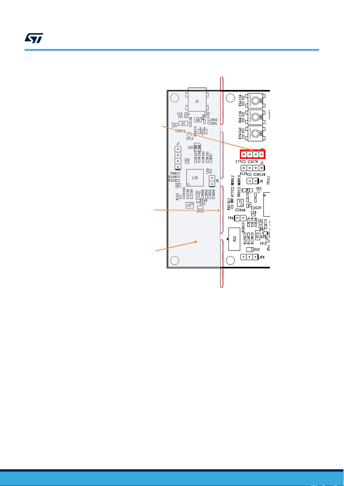
Figure 2 shows the position of the main circuitry blocks of the board.
Figure 2. EVSPIN32F06Q1S3 --board functions
UM2835
Hardware description and configuration
Figure 3
shows the position of the connectors and jumpers of the board.
Figure 3. EVSPIN32F06Q1S3 - main components and connector positions
UM2835 - Rev 1
page 7/19
Page 8
UM2835
Hardware description and configuration
Table 1. Hardware setting jumpers
Jumper Permitted configurations Default condition
JP1 Selection of boot from flash (2-3 closed) or System/SRAM (1-2 closed) 2-3 closed
JP2 Selection hall Encoder power supply to VDD closed
JP3 Selection PA0 connected to Hall 1 closed
JP4 Selection PA1 connected to Hall 2 closed
JP5 Selection PA2 connected to Hall 3 closed
JP6 Selection VBUS feedback partition closed
JP7 Selection Encoder sensor power to VDD (1-2 closed) , VCC (2-3 closed) or +5V (2-4 closed) 2-4 closed
Selection VDD connected to power supply (1-2 closed)
JP8
or STLINK (2-3 closed)
Selection VCC connected to power supply (1-2 closed)
JP9
or external supply (VCC=pin 2 GND=pin 3, jumper removed)
Table 2. Connectors and test points description
1-2 closed
1-2 closed
Name Pin Label Description
J1 1-2-3-4 J1 SPI interface, simulated DAC debug port (pins 3,4) or customizable GPIOs
1 OUT3
J2
3 OUT1
1 A+/H1
J3
J4 1 – 2 J4 - AC MAINS ~ AC mains power supply
J5 - J5 USB input ST-link
J6
J7
J8 1-2 J8 ST-link reset
J9
3 Z+/H3
4 VDD
5 GND
1 RX
2 TX
1
2 SWCLK of ST-link
3 GND
4 SWDIO of ST-link
1 VDD
2 SWD CLK
3 GND
4 SWD IO
J7
Motor phases connections2 OUT2
Hall/encoder sensors connector2 B+/H2
Hall sensors/encoder supply
UART
ST-link power supply
Auxiliary connector for SWD mode debugging/programming
UM2835 - Rev 1
page 8/19
Page 9

Hardware description and configuration
Table 3. Test points description
Name Pin Label Description
TP1 - TP1 RES1
TP2 - TP2 RES2
TP3 TP3 RES3
TP4 - TP4 OUT 3
TP5 - TP5 PB8 GPIO
TP6 - TP6 PA4 GPIO, PA3 GPIO (SPEED)
TP7 - TP7 OUT 2
TP8 - TP8 GND – signal ground
TP12 - TP12 OD – SmartSD timing open drain output
TP14 - TP14 OUT 1
TP15 - TP15 3V3 STLINK USB voltage
TP18 - TP18 PGND – power ground
TP19 - TP19 High side channel 3 gate
TP20 - TP20 Low side channel 3 gate
TP21 - TP21 High side channel 2 gate
TP22 - TP22 Low side channel 2 gate
TP23 - TP23 High side channel 1 gate
TP24 - TP24 Low side channel 1 gate
TP25 - TP25 SENSE channel 1
TP26 - TP26 SENSE channel 2
TP27 - TP27 SENSE channel 3
TP28 - TP28 PA12 GPIO
TP29 - TP29 CIN – comparator positive input
UM2835
UM2835 - Rev 1
page 9/19
Page 10
6 Board description
6.1 Sensorless
The evaluation board can be used in FOC sensorless mode without modifications, current signals are read
through shunt resistors, amplified and brought to MCU ADC channels 5, 6 and 7.
6.2 Hall/Encoder motor speed sensor
The EVSPIN32F06Q1S3 evaluation board supports the digital Hall and quadrature encoder sensors for motor
position feedback.
Sensors can be connected to the STSPIN32F0601Q through the J3 connector as listed in the following table.
Table 4. Hall/Encoder connector (J3)
Name Pin Description
Hall1/A+ 1 Hall sensor 1/Encoder out A+
Hall2/B+ 2 Hall sensor 2/Encoder out B+
Hall3/Z+ 3 Hall sensor 3/Encoder Zero feedback
VDD_sensor 4 Sensor supply voltage
GND 5 Ground
UM2835
Board description
6.3
A protection resistor of 1.8 kΩ is mounted in series with sensor outputs.
For sensors requiring external pull-up, three 10 kΩ resistors are already mounted on the output lines and
connected to VDD voltage when JP2 is closed.
The jumper JP7 selects the power supply for sensor supply voltage:
• JP7 pins 1-2 CLOSED : Hall sensors powered by VDD ( 3.3 V )
• JP7 pins 2-3 CLOSED : Hall sensors powered by VCC ( 15 V )
• JP7 pins 2-4 CLOSED : Hall sensors powered by V5_Hall (+5 V)
The MCU of STSPIN32F0601Q can decode Hall/Encoder sensor outputs configuring jumpers as follows:
• JP3 CLOSED, PA0 connected to Hall1
• JP4 CLOSED, PA1 connected to Hall2
• JP5 CLOSED, PA2 connected to Hall3
Overcurrent detection and current sensing measurement
The EVSPIN32F06Q1S3 evaluation board implements overcurrent protection based on the STSPIN32F0601Q
integrated comparator. The shunt resistors measures the load current bringing the voltage signal associated to
load current to the CIN pin (TP29). When the peak current in the phases exceeds the selected threshold, the
integrated comparator is triggered and all the power switches are disabled. Power switches are enabled again
when the current falls below the threshold and the output disable time expires, thus implementing a current
limitation control.
UM2835 - Rev 1
page 10/19
Page 11

Current sensing circuitry
Output disable time
circuitry
Overcurrent detection and current sensing measurement
Figure 4. EVSPIN32F06Q1S3 - Current sensing and disable time circuitry
UM2835
By default the evaluation board has an overcurrent threshold set to I
= 4.5 A and a restart time after fault
OC_typ
detection of ~560us
Overcurrent threshold can be modified changing R49 bias resistor, R57, R50, R51 loop resistors and R33, R53,
R56 shunt resistors according to the following formulas:
• V
• R
=460mV, VDD=3.3V
REF_typ
= R33=R53=R56 = 220mΩ
SHUNT
• RPU=R49=10kΩ
• R
• If R
=R57=R50=R51=1kΩ
LOOP
<< R
SHUNT
LOOP
:
I
OC_typ
≅ V
REF_typ
3RPU+ R
⋅
R
SHUNT
LOOP
⋅ R
PU
− VDD ⋅
R
SHUNT
R
LOOP
⋅ R
PU
The output disable time can be monitored on the OD pin (TP12) and is determined mainly by the time required to
recharge the C18 capacitor up to V
• V
• V
SSDh
SSDl
=3.8V
=0.56V
threshold, according to the formulas:
SSDh
• VOD=VCC=15V
V
t2≅ C18 ⋅ R49 ⋅ ln
SSDl −VOD
V
− V
SSDh
OD
(1)
(2)
UM2835 - Rev 1
page 11/19
Page 12

6.4 Bus voltage circuit
The EVSPIN32F06Q1S3 evaluation board provides the bus voltage sensing. This signal is set through a voltage
divider from motor supply voltage (VBUS) (R67, R69 and R78, R80), and sent to PB1 GPIO (channel 9 of the
ADC) of the embedded MCU.
• JP6 closed (by default) allows to set the bus voltage divider to 145
• JP6 open allows to set the bus voltage divider to 126
6.5 Hardware user interface
The board provides a hardware user interface as follows
• a potentiometer R23 setting, for example, the target speed
• switch SW1 : reset STSPIN32F0601Q MCU
• switch SW2 : user button 2
• switch SW3 : user button 1
• LED DL1: turned on when user 2 button is pressed
• LED DL2: turned on when user 1 button is pressed
• LED DL3: turned on when VDD is on (MCU stage powered )
LED LD2: turned on when VCC flyback is on (Gate Driver stage powered)
UM2835
Bus voltage circuit
6.6 Debug
The EVSPIN32F06Q1S3 evaluation board embeds an ST-LINK/V2-1 debugger/programmer. The features
supported by ST-LINK are:
• USB software re-enumeration
• Virtual com port interface on USB connected to PB6/PB7 pins of the STSPIN32F0601Q (UART1)
• Mass storage interface on USB
The power supply for ST-LINK is provided by the host PC through the USB cable connected to J5.
LED LD1 provides ST-LINK communication status information:
• Red LED flashing slowly: at power-on before USB initialization
• Red LED flashing quickly: following first correct communication between the PC and ST-LINK/V2-1
(enumeration)
• Red LED ON: initialization between the PC and ST-LINK/V2-1 is complete
• Green LED ON: successful target communication initialization
• Red/Green LED flashing: during communication with target
• Green ON: communication finished and successful.
The reset function is disconnected from ST-LINK by removing jumper J8.
6.7 ST-LINK detachable
Once the evaluation board is programmed, it is possible to detach the ST-LINK debugger, breaking the PCB
along slot holes. The capability to program or debug STSPIN32F0601Q is still allowed by connecting an external
ST-LINK to J9 SWD connector.
UM2835 - Rev 1
page 12/19
Page 13
Slot holes to
detach ST-Link
J9 SWD
connector
Detachable
section ST-Link
debugger
Using an external DC power supply
Figure 5. EVSPIN32F06Q1S3 - detachable section
UM2835
6.8 Using an external DC power supply
UM2835 - Rev 1
The EVSPIN32F06Q1S3 evaluation board generates VDD=3.3 V and VCC=15 V through a flyback converter by
default.
Optionally it can be configured to provide VDD and VCC through external power supply
• VCC is provided removing JP9 and connecting pin2 to the external supply (e.g. 12 V) and pin3 to GND.
• VDD can be provided by ST-LINK through JP8 (2-3 CLOSED) or connecting JP8 pin2 to 3.3 V and GND to
TP8
page 13/19
Page 14

7 References
This user manual provides information on the hardware features and use of the EVSPIN32F06Q1S3 evaluation
board. For additional information refer to:
• EVSPIN32F06Q1S3 Data brief (schematics, bill of material, layout)
• STSPIN32F0601Q Datasheet
• STGD6M65DF2 Datasheet
• User manual ST-LINKV2 programmer
UM2835
References
UM2835 - Rev 1
page 14/19
Page 15

Revision history
UM2835
Table 5. Document revision history
Date Version Changes
01-Apr-2021 1 Initial release.
UM2835 - Rev 1
page 15/19
Page 16

UM2835
Contents
Contents
1 Main features ......................................................................2
1.1 Target applications .............................................................2
2 Safety and operating instructions ..................................................3
2.1 General terms .................................................................3
2.2 Intended use of evaluation board .................................................3
2.3 Installing the evaluation board....................................................3
2.4 Operating the evaluation board ...................................................3
3 Hardware and software requirements ..............................................5
4 Getting started ....................................................................6
5 Hardware description and configuration ...........................................7
6 Board description ................................................................10
6.1 Sensorless ...................................................................10
6.2 Hall/Encoder motor speed sensor................................................10
6.3 Overcurrent detection and current sensing measurement ............................10
6.4 Bus voltage circuit .............................................................12
6.5 Hardware user interface ........................................................12
6.6 Debug .......................................................................12
6.7 ST-LINK detachable ...........................................................12
6.8 Using an external DC power supply ..............................................13
7 References .......................................................................14
Revision history .......................................................................15
Contents ..............................................................................16
List of tables ..........................................................................17
List of figures..........................................................................18
UM2835 - Rev 1
page 16/19
Page 17

UM2835
List of tables
List of tables
Table 1. Hardware setting jumpers ..............................................................8
Table 2. Connectors and test points description .....................................................8
Table 3. Test points description ................................................................9
Table 4. Hall/Encoder connector (J3) ........................................................... 10
Table 5. Document revision history ............................................................. 15
UM2835 - Rev 1
page 17/19
Page 18

UM2835
List of figures
List of figures
Figure 1. EVSPIN32F06Q1S3 evaluation board ....................................................1
Figure 2. EVSPIN32F06Q1S3 --board functions ....................................................7
Figure 3. EVSPIN32F06Q1S3 - main components and connector positions .................................7
Figure 4. EVSPIN32F06Q1S3 - Current sensing and disable time circuitry................................. 11
Figure 5. EVSPIN32F06Q1S3 - detachable section ................................................ 13
UM2835 - Rev 1
page 18/19
Page 19

UM2835
IMPORTANT NOTICE – PLEASE READ CAREFULLY
STMicroelectronics NV and its subsidiaries (“ST”) reserve the right to make changes, corrections, enhancements, modifications, and improvements to ST
products and/or to this document at any time without notice. Purchasers should obtain the latest relevant information on ST products before placing orders. ST
products are sold pursuant to ST’s terms and conditions of sale in place at the time of order acknowledgement.
Purchasers are solely responsible for the choice, selection, and use of ST products and ST assumes no liability for application assistance or the design of
Purchasers’ products.
No license, express or implied, to any intellectual property right is granted by ST herein.
Resale of ST products with provisions different from the information set forth herein shall void any warranty granted by ST for such product.
ST and the ST logo are trademarks of ST. For additional information about ST trademarks, please refer to www.st.com/trademarks. All other product or service
names are the property of their respective owners.
Information in this document supersedes and replaces information previously supplied in any prior versions of this document.
© 2021 STMicroelectronics – All rights reserved
UM2835 - Rev 1
page 19/19
 Loading...