

Page 1
UM2849
User manual
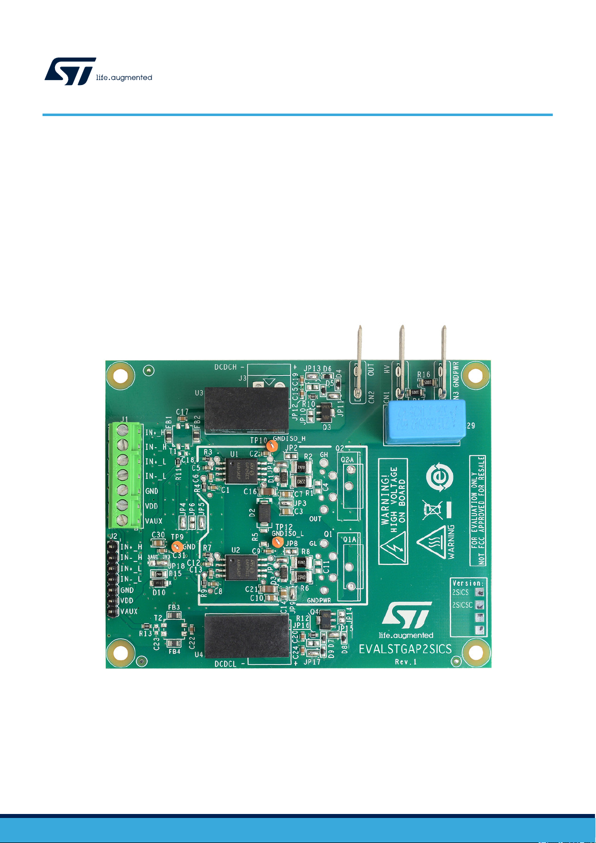
EVALSTGAP2SICS: isolated 4 A single gate driver demonstration board
Introduction
The EVALSTGAP2SICS board allows evaluating all the STGAP2SICS features while driving a half-bridge power stage with
voltage rating up to 1200 V in a TO-220 or TO-247 package.
This document refers to both the EVALSTGAP2SICS and EVALSTGAP2SICSC board because the two boards are the same
with different default configuration (see Table 2 and Table 7).
The board allows easily selecting and modifying the values of the relevant external components in order to facilitate the driver’s
performance evaluation under different applicative conditions and fine pre-tuning of the final application’s components.
Figure 1. EVALSTGAP2SICS demonstration board
UM2849 - Rev 1 - March 2021
For further information contact your local STMicroelectronics sales office.
www.st.com
Page 2
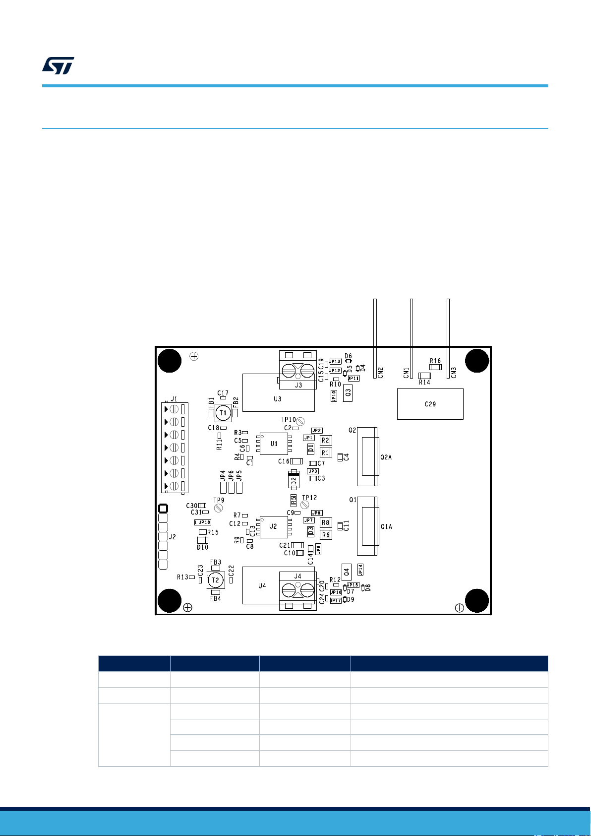
1 Board description and configuration
The board allows tuning several design parameters, giving the possibility to evaluate and optimize the
performance and switching characteristics of the power stage.
The user can select and mount the power switch of choice in either a TO-220 or TO-247 package; the board also
allows installing an optional heat-sink.
The demonstration board comes populated with isolated DC-DC converters in the standard SIP7 package to
supply the gate driving section, which significantly reduce the effort to supply the system and allows fast and easy
evaluation of the gate driving performances.
The board is compatible with the whole STGAP2SIC family in an SO-8W package, so it is possible to evaluate the
part number of interest just by replacing the gate driver.
Figure 2 shows the position of the main components and connectors on the board.
Figure 2. EVALSTGAP2SICS – Main components and connectors position
UM2849
Board description and configuration
UM2849 - Rev 1
Table 1. Board connectors
Name
J4 1 - 2 DCDCL Low-side VH supply voltage
J3 1 - 2 DCDCH High-side VH supply voltage
J2
J1
Pin Label Description
1 IN+_H High-side driver logic input, active high
2 IN-_H High-side driver logic input, active low
3 IN+_L Low-side driver logic input, active high
4 IN-_L Low-side driver logic input, active low
page 2/11
Page 3
Logic supply voltage (VDD)
Name Pin Label Description
J2
J1
CN3 1 GNDPWR Power ground
CN2 1 OUT Power stage output
CN1 1 HV High voltage power supply
5 GND Logic ground
6 VDD Logic supply voltage
7 AUX Auxiliary power supply
Table 2. Board jumpers setting
Jumper Permitted configurations Default condition
JP3
JP4 Input signals configuration: IN-_L connected to IN+_H Closed
JP5 Input signals configuration: IN+_L connected to IN-_H Closed
JP6 Input signals configuration: IN-_L connected to IN-_H Open
JP2
JP1
JP8
JP7
JP9
JP14
JP12
JP13
JP10
JP11
JP15
JP17
JP16
JP18 VDD logic supply configuration (refer to Table 3) Closed 2-3
HS gate voltage configuration: selection of negative voltage (refer to
Table 5)
HS gate resistor configuration: connection of CLAMP pin to power
gate
HS gate resistor configuration: connection of GOFF pin to turn-off
gate path
LS gate resistor configuration: connection of CLAMP pin to power
gate
LS gate resistor configuration: connection of GOFF pin to turn-off
gate path
LS gate voltage configuration: selection of negative voltage (refer to
Table 5 )
LS gate voltage configuration: direct connection of DCDCL+ to VH_L
net
HS gate voltage configuration: connection of DCDCH 0V output
reference to OUT net
HS gate voltage configuration: connection of DCDCH- to GNDISO_H
net
HS gate voltage configuration: direct connection of DCDCH+ to
VH_H net
HS gate voltage configuration: selection of positive voltage (refer to
Table 5)
LS gate voltage configuration: selection of positive voltage (refer to
Table 5)
LS gate voltage configuration: connection of DCDCL- to GNDISO_L
net
LS gate voltage configuration: connection of DCDCL 0V output
reference to GNDPWR net
Closed
Open in EVALSTGAP2SICS
Closed in EVALSTGAP2SICSC
Closed in EVALSTGAP2SICS
Open in EVALSTGAP2SICSC
Open in EVALSTGAP2SICS
Closed in EVALSTGAP2SICSC
Closed in EVALSTGAP2SICS
Open in EVALSTGAP2SICSC
Closed
Open
Open
Closed
Open
Closed
Closed
Closed
Open
UM2849
1.1 Logic supply voltage (VDD)
It is possible to provide the gate driver control logic supply VDD in three alternative ways to match driver input
threshold with the controlling signals voltage swing:
UM2849 - Rev 1
page 3/11
Page 4
UM2849
Gate driver supply voltage (VH)
• Using the on-board 3.3 V Zener D10 regulator to supply VDD. The Zener is supplied from DC-DC input
voltage VAUX. So only the 5 V VAUX DC-DC supply input is powered to supply the whole system (default
configuration).
• Supplying externally VDD net from J1 or J2 (pin 6) with a voltage between 3 V and 5.5 V.
• Supplying externally VDD and VAUX together (VDD max. 5.5 V).
In case the default option is not used, it is required to modify JP18 according to Table 3 and R15 according to
Table 4 also to avoid regulator component damage.
Table 3. Logic supply voltage selection (VDD)
VDD JP18 Note
3.3 V, on-board (default) 2-3 closed VDD generated from VAUX with Zener diode D10
3.3 V, external Open VDD directly supplied from J1 or J2 (pin 6)
VDD = VAUX, external 1-2 closed VDD and VAUX (DC-DC supply) tied together by JP18
The R15 resistor value has been selected for using 5 V input DC-DC module. If a different VAUX input voltage is
used, follow Table 4 to modify resistor R15 (which biases Zener D10) to avoid resistor overheating.
Table 4. R17 value selection with a 3.3 V Zener diode D10 regulator
DCDC module supply input voltage VAUX R15 JP18
3.3 V Do not care 1-2 closed
5 V (default) 240 Ω 2-3 closed or JP18 open
12 V 1200 Ω 2-3 closed or JP18 open
15 V 1500 Ω 2-3 closed or JP18 open
24 V 2700 Ω 2-3 closed or JP18 open
1.2 Gate driver supply voltage (VH)
It is possible to provide the gate driver supply voltage VH in several alternative ways:
• Using isolated DC-DC converters in the standard SIP7 package (U3, U4)
• Using the bootstrap diode D2 by supplying the low-side driver via J4 and mounting the resistor R5 (initial
suggested value 10 Ω)
• Supplying directly J3 and J4 connectors (not mounted) with two separated isolated supplies.
The faster, easier and safer way to supply the board is by using isolated DC-DC converters.
The bootstrap diode supplying method is much simpler and less expensive but does not allow evaluating negative
gate driving voltage. The bootstrap diode is 1200 V rated, if a higher bus voltage is required the diode must be
replaced accordingly.
Supplying externally via J3 and J4 is in general not recommended, unless using supplies specifically designed for
this purpose (with high voltage isolation) or batteries.
Supplies provided from the optional DC-DC or from J3 and J4 connectors are post regulated in order to allow an
easy modification of the gate driving voltages. Some predefined supply voltages can be selected through solder
jumpers; further tuning can be made by changing the value of the relevant Zener diodes.
UM2849 - Rev 1
page 4/11
Page 5

UM2849
Drivers logic input signals
Table 5. Gate driving voltage configuration (positive/negative)
Gate driving voltage JP3, JP9 JP11, JP15
+17 V / 0 V (default) Closed Closed
+17 V / -2.7 V Open Closed
+19 V / 0 V Closed Open
+19 / -2.7 V Open Open
The board has been designed for indifferently using 5 V input and 24 V single output or “12 + 12 V” dual output
DC-DCs.
Other output voltage DC-DCs can be used by modifying the post regulation network.
Other input voltage DC-DCs can be used by modifying R15 (see Section 1.1 ).
DC-DC's input voltage is connected to VAUX signal, available on J1 and J2.
DC-DCs with SIP7 footprint are available mostly with 1 W and 2 W output rated power. For most applications, 1 W
power modules are enough.
Especially for high dV/dt applications, low input to output isolation capacitance (referred to as input to output
coupling capacitance) regulators are recommended.
During applicative output transients (dV/dt), the possible noise generated by the isolation capacitance could make
user measurements difficult and noisy. To simplify, user measurements task DC-DC input supply is filtered with
FB1, FB2, FB3 and FB4 ferrite beads. In the final application, beads are usually removed for cost reasons. On the
other hand, if the user wants a still more improved filter, replacing the beads with a common mode filter (T1 and
T2) like, for instance, the TDK ACM4520-142, is suggested.
1.3
Drivers logic input signals
Drivers logic input signals can be applied through the dedicated pins of J1 or J2 connector (refer to Table 1 for
details).
It is possible to reduce the required driving signals exploiting the on-board jumpers according to Table 6.
Input configuration Description Jumper Default condition
IN+_H = IN-_L
IN+_L = IN-_H
IN-_L = IN-_H
The same input signal is applied to IN+ of high-side driver U1 and
IN- of low-side driver U2
The same input signal is applied to IN- of high-side driver U1 and
IN+ of low-side driver U2
The same input signal is applied to IN- of high-side driver U1 and
IN- of low-side driver U2
1.4 Drivers gate resistors
The gate resistors are selected based on the selected power switch and application topology.
It is possible to evaluate different gate drivers of the STGAP2SIC family by setting few jumpers according to
Table 7.
Table 6. Input signals settings
JP4 Closed
JP5 Closed
JP6 Open
UM2849 - Rev 1
page 5/11
Page 6

Table 7. Gate driver resistors and jumper settings
UM2849
Power stage decoupling
Gate driver Feature JP8, JP2 JP1, JP7
STGAP2SICSM
STGAP2ICSCM
(1)
(2)
1. The presence of D1 and D3 does not influence turn-off speed and these diodes are not required in the final application. D1
and D3 are mounted on board to speed up evaluation of STGAP2SC (Miller Clamp version).
2. R2, D1, R8 and D3 are only required if differentiated turn-on and turn-off speed are required by the user.
1.5 Power stage decoupling
As for all switching applications, high voltage supply is properly decoupled and appropriate decoupling capacitor
is connected to the board to reduce bus ringing and power switch overvoltage spikes during operation.
The board is equipped with a small 1.25 kV DC rated film capacitor (C29) in a convenient position to operate the
power switches more safely.
Depending on the application, bus decoupling can be modified also by using the provided footprint and holes for
the bus capacitors C28, C29, C27, C26, C25.
Danger:
DANGER OF DEATH! High voltage present on the board! Before operating on the board, ensure
that all capacitors are discharged.
Turn-on
resistor
Turn-off
resistor
Separated outputs Open Closed R6, R1 R8, R2
Miller Clamp Closed Open R6, R1
R8 // R6
R1 // R2
UM2849 - Rev 1
page 6/11
Page 7

Revision history
UM2849
Table 8. Document revision history
Date Version Changes
12-Mar-2021 1 Initial release.
UM2849 - Rev 1
page 7/11
Page 8

UM2849
Contents
Contents
1 Board description and configuration ...............................................2
1.1 Logic supply voltage (VDD) ......................................................3
1.2 Gate driver supply voltage (VH) ..................................................4
1.3 Drivers logic input signals........................................................5
1.4 Drivers gate resistors ...........................................................5
1.5 Power stage decoupling .........................................................6
Revision history ........................................................................7
Contents ...............................................................................8
List of tables ...........................................................................9
List of figures..........................................................................10
UM2849 - Rev 1
page 8/11
Page 9

UM2849
List of tables
List of tables
Table 1. Board connectors ...................................................................2
Table 2. Board jumpers setting ................................................................3
Table 3. Logic supply voltage selection (VDD) ......................................................4
Table 4. R17 value selection with a 3.3 V Zener diode D10 regulator ......................................4
Table 5. Gate driving voltage configuration (positive/negative) ........................................... 5
Table 6. Input signals settings .................................................................5
Table 7. Gate driver resistors and jumper settings ...................................................6
Table 8. Document revision history ..............................................................7
UM2849 - Rev 1
page 9/11
Page 10

UM2849
List of figures
List of figures
Figure 1. EVALSTGAP2SICS demonstration board..................................................1
Figure 2. EVALSTGAP2SICS – Main components and connectors position .................................2
UM2849 - Rev 1
page 10/11
Page 11

UM2849
IMPORTANT NOTICE – PLEASE READ CAREFULLY
STMicroelectronics NV and its subsidiaries (“ST”) reserve the right to make changes, corrections, enhancements, modifications, and improvements to ST
products and/or to this document at any time without notice. Purchasers should obtain the latest relevant information on ST products before placing orders. ST
products are sold pursuant to ST’s terms and conditions of sale in place at the time of order acknowledgement.
Purchasers are solely responsible for the choice, selection, and use of ST products and ST assumes no liability for application assistance or the design of
Purchasers’ products.
No license, express or implied, to any intellectual property right is granted by ST herein.
Resale of ST products with provisions different from the information set forth herein shall void any warranty granted by ST for such product.
ST and the ST logo are trademarks of ST. For additional information about ST trademarks, please refer to www.st.com/trademarks. All other product or service
names are the property of their respective owners.
Information in this document supersedes and replaces information previously supplied in any prior versions of this document.
© 2021 STMicroelectronics – All rights reserved
UM2849 - Rev 1
page 11/11
 Loading...