


Iso high side smart power solid state relay
Features
Typ e V
VND05BSP 40 V 0.2 Ω 1.6A 26 V
DSSRDS(on)IOUT
VND05BSP
V
CC
10
1
■ Output current (continuous): 9A @ Tc=85°C
■ 5V logic level compatible input
■ Thermal shutdown
■ Under voltage shutdown
■ Open drain diagnostic output
■ Inductive load fast demagnetization
■ Very low standby power dissipation
Table 1. Device summary
Package
PowerSO-10
Description
The VND05BSP is a monolithic device made
using STMicroelectronics VIPower Technology,
intended for driving resistive or inductive loads
with one side grounded.
This device has two channels, and a common
diagnostic. Built-in thermal shutdown protects the
chip from over temperature and short circuit.
The status output provides an indication of open
load in on state, open load in off state,
overtemperature conditions and stuck-on to V
Order codes
Tube Tape & reel
CC.
VND05BSP VND05BSP VND05BSP13TR
November 2008 Rev 3 1/16
www.st.com
16

Contents VND05BSP
Contents
1 Block diagram and pin description . . . . . . . . . . . . . . . . . . . . . . . . . . . . . 5
2 Electrical specifications . . . . . . . . . . . . . . . . . . . . . . . . . . . . . . . . . . . . . . 6
2.1 Absolute maximum ratings . . . . . . . . . . . . . . . . . . . . . . . . . . . . . . . . . . . . . 6
2.2 Thermal data . . . . . . . . . . . . . . . . . . . . . . . . . . . . . . . . . . . . . . . . . . . . . . . 7
2.3 Electrical characteristics . . . . . . . . . . . . . . . . . . . . . . . . . . . . . . . . . . . . . . . 7
3 Application information . . . . . . . . . . . . . . . . . . . . . . . . . . . . . . . . . . . . . 11
3.1 Functional description . . . . . . . . . . . . . . . . . . . . . . . . . . . . . . . . . . . . . . . 12
3.2 Protecting the device against reverse battery . . . . . . . . . . . . . . . . . . . . . 12
4 Package and packing information . . . . . . . . . . . . . . . . . . . . . . . . . . . . . 13
4.1 ECOPACK® packages . . . . . . . . . . . . . . . . . . . . . . . . . . . . . . . . . . . . . . . 13
4.2 PowerSO-10 mechanical data . . . . . . . . . . . . . . . . . . . . . . . . . . . . . . . . . 13
5 Revision history . . . . . . . . . . . . . . . . . . . . . . . . . . . . . . . . . . . . . . . . . . . 15
2/16

VND05BSP List of tables
List of tables
Table 1. Device summary . . . . . . . . . . . . . . . . . . . . . . . . . . . . . . . . . . . . . . . . . . . . . . . . . . . . . . . . . . 1
Table 2. Absolute maximum ratings . . . . . . . . . . . . . . . . . . . . . . . . . . . . . . . . . . . . . . . . . . . . . . . . . . 6
Table 3. Thermal data. . . . . . . . . . . . . . . . . . . . . . . . . . . . . . . . . . . . . . . . . . . . . . . . . . . . . . . . . . . . . 7
Table 4. Power . . . . . . . . . . . . . . . . . . . . . . . . . . . . . . . . . . . . . . . . . . . . . . . . . . . . . . . . . . . . . . . . . . 7
Table 5. Switching (V
Table 6. Logic inputs. . . . . . . . . . . . . . . . . . . . . . . . . . . . . . . . . . . . . . . . . . . . . . . . . . . . . . . . . . . . . . 8
Table 7. Protections and diagnostics . . . . . . . . . . . . . . . . . . . . . . . . . . . . . . . . . . . . . . . . . . . . . . . . . 8
Table 8. Truth table. . . . . . . . . . . . . . . . . . . . . . . . . . . . . . . . . . . . . . . . . . . . . . . . . . . . . . . . . . . . . . 10
Table 9. PowerSO-10 mechanical data . . . . . . . . . . . . . . . . . . . . . . . . . . . . . . . . . . . . . . . . . . . . . . 14
Table 10. Document revision history . . . . . . . . . . . . . . . . . . . . . . . . . . . . . . . . . . . . . . . . . . . . . . . . . 15
=13V) . . . . . . . . . . . . . . . . . . . . . . . . . . . . . . . . . . . . . . . . . . . . . . . . . . . . . . 7
CC
3/16

List of figures VND05BSP
List of figures
Figure 1. Block diagram . . . . . . . . . . . . . . . . . . . . . . . . . . . . . . . . . . . . . . . . . . . . . . . . . . . . . . . . . . . . 5
Figure 2. Configuration diagram (top view) . . . . . . . . . . . . . . . . . . . . . . . . . . . . . . . . . . . . . . . . . . . . . 5
Figure 3. Current and voltage conventions . . . . . . . . . . . . . . . . . . . . . . . . . . . . . . . . . . . . . . . . . . . . . 6
Figure 4. I
Figure 5. t
Figure 6. Switching time waveforms . . . . . . . . . . . . . . . . . . . . . . . . . . . . . . . . . . . . . . . . . . . . . . . . . . 9
Figure 7. Waveforms . . . . . . . . . . . . . . . . . . . . . . . . . . . . . . . . . . . . . . . . . . . . . . . . . . . . . . . . . . . . . 10
Figure 8. Typical application circuit with a schottky diode for reverse supply protection . . . . . . . . . . 11
Figure 9. Typical application circuit with separate signal ground . . . . . . . . . . . . . . . . . . . . . . . . . . . . 11
Figure 10. PowerSO-10 package dimensions . . . . . . . . . . . . . . . . . . . . . . . . . . . . . . . . . . . . . . . . . . . 13
circuit . . . . . . . . . . . . . . . . . . . . . . . . . . . . . . . . . . . . . . . . . . . . . . . . . . . . . . . . . . . . . . 9
L(off)
pol/tpovl
waveforms . . . . . . . . . . . . . . . . . . . . . . . . . . . . . . . . . . . . . . . . . . . . . . . . . . . . . . . . 9
4/16
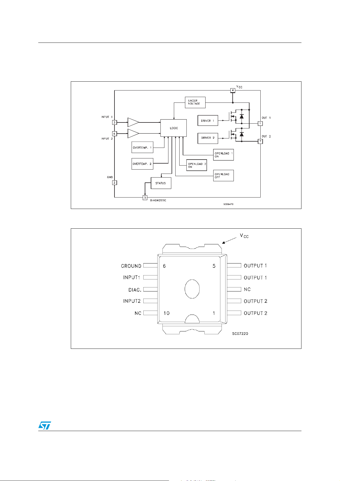
VND05BSP Block diagram and pin description
1 Block diagram and pin description
Figure 1. Block diagram
Figure 2. Configuration diagram (top view)
5/16

Electrical specifications VND05BSP
2 Electrical specifications
Figure 3. Current and voltage conventions
2.1 Absolute maximum ratings
Stressing the device above the rating listed in the “Absolute maximum ratings” table may
cause permanent damage to the device. These are stress ratings only and operation of the
device at these or any other conditions above those indicated in the operating sections of
this specification is not implied. Exposure to Absolute maximum rating conditions for
extended periods may affect device reliability. Refer also to the STMicroelectronics sure
program and other relevant quality document.
Table 2. Absolute maximum ratings
Symbol Parameter Value Unit
V
(BR)DSS
I
OUT
I
OUT (RMS)
I
R
I
IN
-V
CC
I
STAT
V
ESD
Ptot Power dissipation at T
Tj Junction operating temperature -40 to 150 °C
Tstg Storage temperature -55 to 150 °C
Drain-Source breakdown voltage 40 V
Output current (cont.) at Tc=85°C 9 A
RMS output current at Tc=85°C and f> 1Hz 9 A
Reverse output current at Tc=85°C -9 A
Input current ±10 mA
Reverse supply voltage -4 V
Status current ±10 mA
Electrostatic discharge (1.5 kΩ, 100 pF) 2000 V
c = 25 °C 59 W
6/16

VND05BSP Electrical specifications
2.2 Thermal data
Table 3. Thermal data
Symbol Parameter Max. value Unit
R
thj-case
R
thj-amb
Thermal resistance junction-case 2.1 °C/W
Thermal resistance junction-ambient 50 °C/W
2.3 Electrical characteristics
Values specified in this section are for 8<VCC<16V; -40°C<Tj<125°C, unless otherwise
stated.
Table 4. Power
Symbol Parameter Test conditions Min. Typ. Max. Unit
V
I
n
Ron On state resistance
V
DS(MAX)
Supply voltage 6 13 26 V
CC
(1)
Nominal current
T
V
I
OUT
Tj = 25°C
I
Supply current
S
Maximum voltage drop
Output to GND internal
Ri
impedance
Off state Tj = 25 °C
V
I
OUT
V
Tj = 25 °C 5 10 20 KΩ
=85°C V
C
CC
CC
=13V
=I
n; VCC
=13V
DS(on)
=13V
=7.5 A; Tj = 85°C
=13V
CC
<0.5
1.6 2.6 A
0.13 0.2 Ω
35 100 µA
1.44 2.3 V
1. In= Nominal current according to ISO definition for high side automotive switch(Tc = 85 oC for battery voltage of 13V which
produces a voltage drop of 0.5 V).
Table 5. Switching (VCC=13V)
Symbol Parameter Test conditions Min. Typ. Max. Unit
= 5.4 Ω
R
OUT
(see
= 5.4 Ω 10 50 180 µs
R
OUT
= 5.4 Ω 10 75 250 µs
R
OUT
R
= 5.4 Ω 10 35 180 µs
OUT
= 5.4 Ω 0.003 0.1
OUT
= 5.4 Ω 0.005 0.1
OUT
525200µs
A/µs
A/µs
A/µs
A/µs
dV
dV
t
d(on)
t
d(off)
OUT
OUT
Turn-on delay time of
output current
t
r
Rise time of output
current
Turn-off delay time of
output current
t
f
/dt
/dt
Fall time of output
current
Turn-on current slope R
(on)
Turn-off current slope R
(off)
7/16

Electrical specifications VND05BSP
Table 6. Logic inputs
Symbol Parameter Test conditions Min. Typ. Max. Unit
V
IL
V
IH
V
I(hyst.)
I
IN
V
ICL
1. The VIH is internally clamped at 6V about. It is possible to connect this pin to an higher voltage via an external resistor
calculated to not exceed 10 mA at the input pin.
Table 7. Protections and diagnostics
Input low level voltage 1.5 V
(1)
Input high level voltage 3.5 V
Input hysteresis voltage 0.2 0.9 1.5 V
Input current VIN = 5 V; Tj= 25°C 30 100 µA
Input clamp voltage
IIN = 10 mA
= -10 mA
I
IN
56
-0.7
7V
Symbol Parameter Test conditions Min. Typ. Max. Unit
V
STAT
V
USD
V
SCL
T
TSD
T
TSD(hyst)
Status voltage output low I
= 1.6 mA 0.4 V
STAT
Under voltage shutdown 3.5 4.5 6 V
Status clamp voltage
Thermal shutdown
temperature
STAT
I
STAT
= 10 mA
= -10 mA
56
-0.7
140 160 180 °C
I
Thermal shutdown
hysteresis
7V
50 °C
V
V
t
povl
t
T
V
I
pol
Reset temperature 125 °C
R
Open voltage level Off-state
OL
Open load current
OL
level
(2)
Status delay
(2)
Status delay
1. IOL(off) = (VCC -VOL)/ROL
2. ISO definition.
(1)
2.5 4 5 V
On-state 5 180 mA
8/16

VND05BSP Electrical specifications
Figure 4. I
Figure 5. t
circuit
L(off)
pol/tpovl
waveforms
Figure 6. Switching time waveforms
9/16

Electrical specifications VND05BSP
Table 8. Truth table
Conditions Input 1 Input 2 Output 1 Output 2 Diagnostic
Normal operation
L
H
L
H
L
H
L
H
Undervoltage X X L L H
Channel 1 H X L X L
Thermal shutdown
Channel 2 X H X L L
Openload
Output shorted to V
CC
Channel 1
Channel 2
Channel 1
Channel 2
H
L
X
L
H
L
X
L
X
L
H
L
X
L
H
L
H
L
X
L
H
H
X
L
X
L
H
L
X
L
H
H
Figure 7. Waveforms
H
H
L
L
L
L
L
L
L
L
10/16

VND05BSP Application information
3 Application information
Figure 8. Typical application circuit with a schottky diode for reverse supply protection
Figure 9. Typical application circuit with separate signal ground
11/16

Application information VND05BSP
3.1 Functional description
The device has a diagnostic output which indicates open load in on-state, open load in offstate, over temperature conditions and stuck-on to V
From the falling edge of the input signal, the status output, initially low to signal a fault
condition (overtemperature or open load on-state), will go back to a high state with a
different delay in case of overtemperature (tpovl) and in case of open open load (tpol)
respectively.
This feature allows to discriminate the nature of the detected fault. To protect the device
against short circuit and over current condition, the thermal protection turns the integrated
Power MOSFET off at a minimum junction temperature of 140°C. When this temperature
returns to 125°C the switch is automatically turned on again. In short circuit the protection
reacts with virtually no delay, the sensor being located inside the Power MOSFET area. An
internal function of the devices ensures the fast demagnetization of inductive loads with a
typical voltage (V
demag) of -18V. This function allows to greatly reduces the power dissipation
according to the formula:
P
dem = 0.5 • Lload •(Ι load)2 • [(VCC+Vdemag)/Vdemag] • f
CC
.
where f = switching frequency and V
demag = demagnetization voltage.
The maximum inductance which causes the chip temperature to reach the shut-down
temperature in a specified thermal environment is a function of the load current for a fixed
V
, Vdemag and f according to the above formula. In this device if the GND pin is
CC
disconnected, with V
not exceeding 16V, it will switch off.
CC
3.2 Protecting the device against reverse battery
The simplest way to protect the device against a continuous reverse battery voltage (-26V)
is to insert a Schottky diode between pin 1 (GND) and ground, as shown in the typical
application circuit (Figure 8.).
The consequences of the voltage drop across this diode are as follows:
● If the input is pulled to power GND, a negative voltage of -VF is seen by the device. (VIL,
V
IH thresholds and VSTAT are increased by VF with respect to power GND).
● The undervoltage shutdown level is increased by VF.
If there is no need for the control unit to handle external analog signals referred to the power
GND, the best approach is to connect the reference potential of the control unit to node [1]
(see Figure 9.), which becomes the common signal GND for the whole control board. In this
way no shift of V
pin; this solution allows the use of a standard diode, with a breakdown voltage able to
handle any ISO normalized negative pulses that occours in the automotive environment.
IH, VIL and VSTAT takes place and no negative voltage appears on the INPUT
12/16

VND05BSP Package and packing information
4 Package and packing information
4.1 ECOPACK® packages
In order to meet environmental requirements, ST offers these devices in ECOPACK®
packages. ECOPACK
®
packages are lead-free. The category of Second Level Interconnect
is marked on the package and on the inner box label, in compliance with JEDEC Standard
JESD97. The maximum ratings related to soldering conditions are also marked on the inner
box label.
ECOPACK is an ST trademark. ECOPACK specifications are available at www.st.com.
4.2 PowerSO-10 mechanical data
Figure 10. PowerSO-10 package dimensions
10
HE
h
A
F
A1
1
eB
0.25
D
= =
D1
= =
E2
DETAIL "A"
B
0.10 A
E
SEATING
PLANE
A
C
B
E4
SEATING
PLANE
A1
DETAIL "A"
L
α
13/16

Package and packing information VND05BSP
Table 9. PowerSO-10 mechanical data
mm
Dim.
Min. Typ. Max.
A 3.35 3.65
(1)
A
A1 0 0.10
B 0.40 0.60
(1)
B
C 0.35 0.55
(1)
C
D 9.40 9.60
D1 7.40 7.60
E 9.30 9.50
3.4 3.6
0.37 0.53
0.23 0.32
E2 7.20 7.60
(1)
E2
E4 5.90 6.10
(1)
E4
e1.27
F 1.25 1.35
(1)
F
H 13.80 14.40
(1)
H
h0.50
L 1.20 1.80
(1)
L
α 0° 8°
(1)
α
1. Muar only POA P013P.
7.30 7.50
5.90 6.30
1.20 1.40
13.85 14.35
0.80 1.10
2° 8°
14/16

VND05BSP Revision history
5 Revision history
Table 10. Document revision history
Date Revision Changes
Apr-2001 1 Initial release.
03-May-2006 2
24-Nov-2008 3
Added contents, list of tables and figures.
Added Table 10.: Document revision history.
Document reformatted and restructured.
Added Table 1.: Device summary.
Added ECOPACK® packages information.
15/16

VND05BSP
Please Read Carefully:
Information in this document is provided solely in connection with ST products. STMicroelectronics NV and its subsidiaries (“ST”) reserve the
right to make changes, corrections, modifications or improvements, to this document, and the products and services described herein at any
time, without notice.
All ST products are sold pursuant to ST’s terms and conditions of sale.
Purchasers are solely responsible for the choice, selection and use of the ST products and services described herein, and ST assumes no
liability whatsoever relating to the choice, selection or use of the ST products and services described herein.
No license, express or implied, by estoppel or otherwise, to any intellectual property rights is granted under this document. If any part of this
document refers to any third party products or services it shall not be deemed a license grant by ST for the use of such third party products
or services, or any intellectual property contained therein or considered as a warranty covering the use in any manner whatsoever of such
third party products or services or any intellectual property contained therein.
UNLESS OTHERWISE SET FORTH IN ST’S TERMS AND CONDITIONS OF SALE ST DISCLAIMS ANY EXPRESS OR IMPLIED
WARRANTY WITH RESPECT TO THE USE AND/OR SALE OF ST PRODUCTS INCLUDING WITHOUT LIMITATION IMPLIED
WARRANTIES OF MERCHANTABILITY, FITNESS FOR A PARTICULAR PURPOSE (AND THEIR EQUIVALENTS UNDER THE LAWS
OF ANY JURISDICTION), OR INFRINGEMENT OF ANY PATENT, COPYRIGHT OR OTHER INTELLECTUAL PROPERTY RIGHT.
UNLESS EXPRESSLY APPROVED IN WRITING BY AN AUTHORIZED ST REPRESENTATIVE, ST PRODUCTS ARE NOT
RECOMMENDED, AUTHORIZED OR WARRANTED FOR USE IN MILITARY, AIR CRAFT, SPACE, LIFE SAVING, OR LIFE SUSTAINING
APPLICATIONS, NOR IN PRODUCTS OR SYSTEMS WHERE FAILURE OR MALFUNCTION MAY RESULT IN PERSONAL INJURY,
DEATH, OR SEVERE PROPERTY OR ENVIRONMENTAL DAMAGE. ST PRODUCTS WHICH ARE NOT SPECIFIED AS "AUTOMOTIVE
GRADE" MAY ONLY BE USED IN AUTOMOTIVE APPLICATIONS AT USER’S OWN RISK.
Resale of ST products with provisions different from the statements and/or technical features set forth in this document shall immediately void
any warranty granted by ST for the ST product or service described herein and shall not create or extend in any manner whatsoever, any
liability of ST.
ST and the ST logo are trademarks or registered trademarks of ST in various countries.
Information in this document supersedes and replaces all information previously supplied.
The ST logo is a registered trademark of STMicroelectronics. All other names are the property of their respective owners.
© 2008 STMicroelectronics - All rights reserved
STMicroelectronics group of companies
Australia - Belgium - Brazil - Canada - China - Czech Republic - Finland - France - Germany - Hong Kong - India - Israel - Italy - Japan -
Malaysia - Malta - Morocco - Singapore - Spain - Sweden - Switzerland - United Kingdom - United States of America
www.st.com
16/16
 Loading...