

现货库存、技术资料、百科信息、热点资讯,精彩尽在鼎好!
VIPer53DIP
®
TYPICAL OUTPUT POWER CAPABILITY
TYPE
European
(195 - 265 Vac)
DIP-8 50W 30W
PowerSO-10
™
Note: Above power capabilities are given under adequate
thermal conditions
65W 40W
US / Wide range
(85 - 265 Vac)
FEATURES
n
SWITCHING FREQUENCY UP TO 300 kHz
n
CURRENT LIMITATION
n
CURRENT MODE CONTROL WITH
ADJUSTABLE LIMITATION
n
SOFT START AND SHUT DOWN CONTROL
n
AUTOMATIC BURST MODE IN STAND-BY
CONDITION (“BLUE ANGEL” COMPLIANT)
n
UNDERVOLTAGE LOCKOUT WITH
HYSTERESIS
n
HIGH VOLTAGE STARTUP CURRENT
SOURCE
n
OVERTEMPERATUR E PR O TECTION
n
OVERLOAD AND SHORT-CIRCUIT CONTROL
VIPer53SP
OFF LINE PRIMARY SWITCH
10
1
DIP-8
DESCRIPTION
The VIPer53 combines in the same package an
enhanced current mode PWM controller with a
high voltage MDMesh Power Mosfet. Typical
applications cover off line power supplies with a
secondary power capability ranging up to 30W in
wide range input voltage or 50W in single
European voltage range and DIP-8 package, with
the following benefits:
– Overload and short circuit controlled by
feedback monitoring and delayed device reset.
– Efficient standby mode by enhanced pulse
skipping.
– Primary regulation or secondary loop failure
protection through high gain error amplifier.
PowerSO-10™
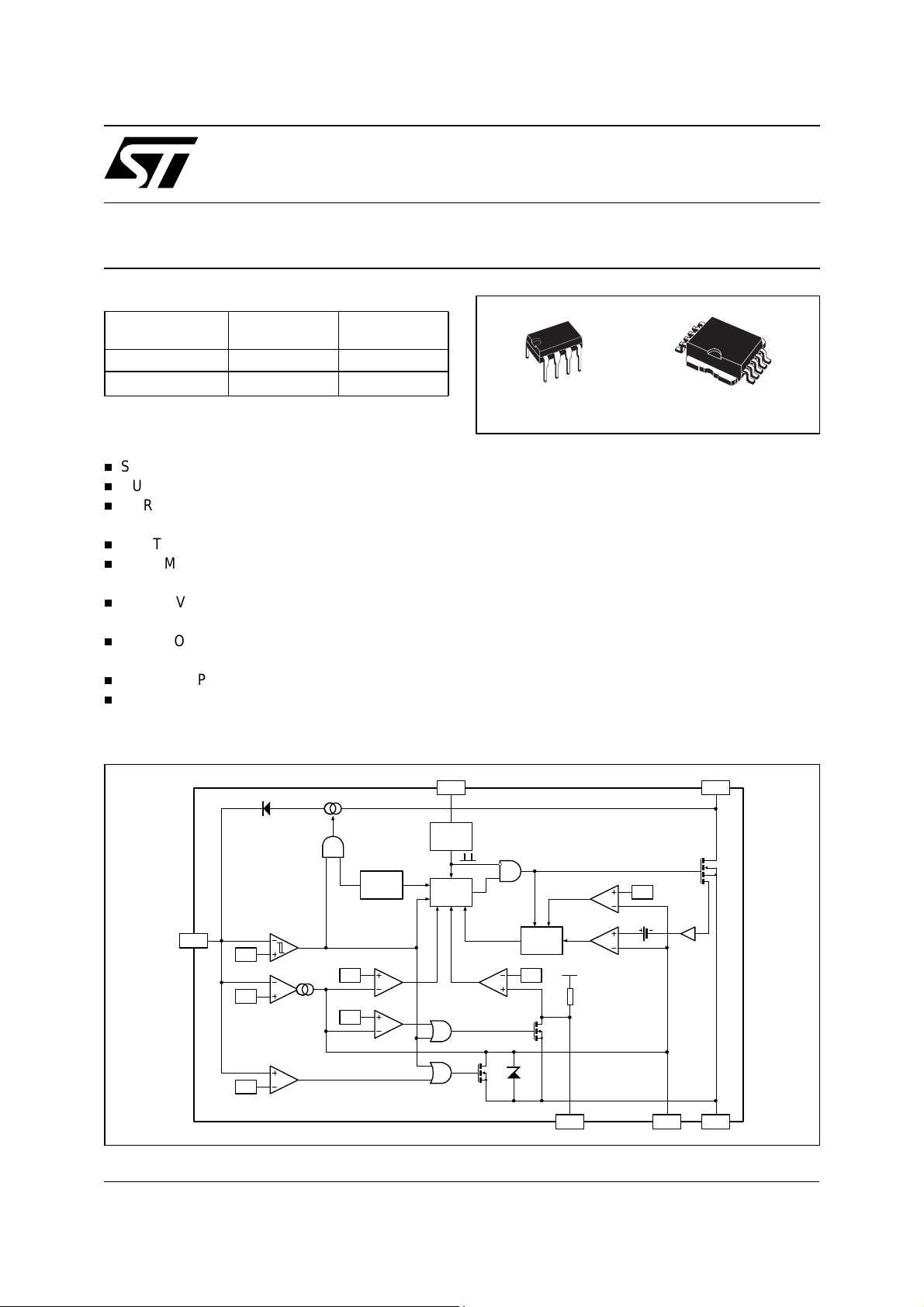
BLOCK DIAGRAM
OSC DRAIN
ON/OFF
OSCILLATOR
PWM
STANDBY
OVERLOAD
LATCH
S
R1
FF
R2
R3 R4 R5
BLANKING TIME
Q
4.5V
SELECTION
150/400ns
BLANKING
4V
PWM
COMPARATOR
8V
125k
TOVL COMP SOURCE
1V
H
0.5V
COMP
CURRENT
AMPLIFIER
OVERTEMP.
DETECTOR
UVLO
11.5V
8.4/
15V
18V
COMPARATOR
ERROR
AMPLIFIER
OVERVOLTAGE
COMPARATOR
0.5V
4.35V
COMPARATOR
COMPARATOR
VDD
June 2004 1/24
VIPer53DIP / VIPer53SP
PIN FUNCTION
Name Function
Power supply of the control circuits. Also provides the charging current of the external capacitor during
start-up. The functions of this pin are managed by four threshold voltages:
: Voltage value at which the device starts switching (Typically 11.5 V).
- V
V
DD
SOURCE Power Mosfet source and circuit ground reference.
DRAIN
COMP
TOVL
OSC Allows the setting of the switching frequency through an external Rt-Ct network.
DDon
- V
: Voltage value at which the device stops switching (Typically 8.4 V).
DDoff
- V
- V
: Regulation voltage point when working in primary feedback (Trimmed to 15 V).
DDreg
: Triggering voltage of the overvoltage protection (Trimmed to 18 V).
DDovp
Power Mosfet drain. Also used by the internal high voltage current source during the start-up phase, for
charging the external V
capacitor.
DD
Input of the current mode structure, and output of the internal error amplifier. Allows the setting of the
dynamic characteristic of the converter through an external passive network. Useful voltage range
extends from 0.5 V to 4.5 V. The Power Mosfet is always off below 0.5 V, and the overload protection is
triggered if the voltage exceeds 4.35V. This action is delayed by the timing capacitor connected to the
TOVL pin.
Allows the connection of an external capacitor for delaying the overload protection, which is triggered by
a voltage on the COMP pin higher than 4.35V.
CURRENT AND VOLTAGE CONVENTIONS
I
DD
I
OSC
OSC
V
DD
V
OSC
V
TOVL
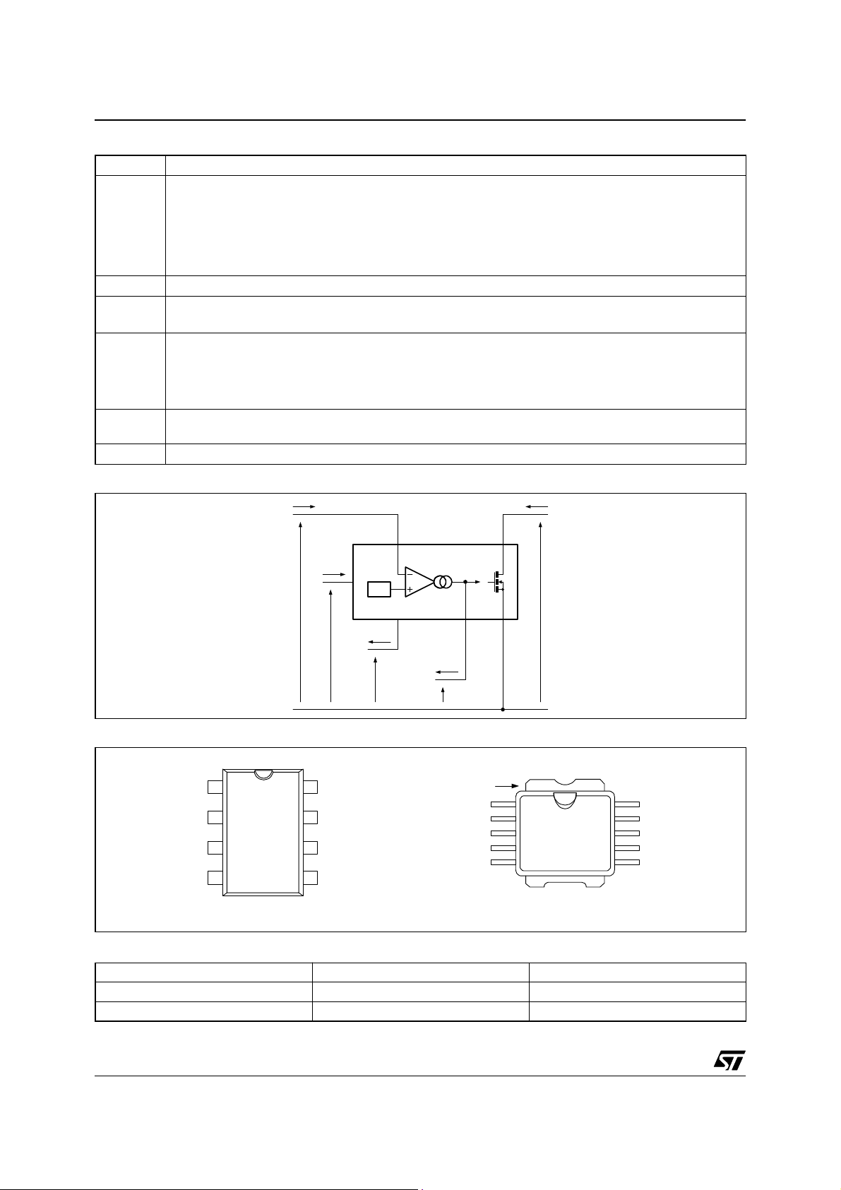
CONNECTION DIAGRAM
OSC
SOURCE
SOURCE
1
2
3
8
TOVLCOMP
7
VDD
6
NC
DRAIN
54
I
D
VDD
15V
I
TOVL
V
COMP
DRAIN
V
SOURCECOMPTOVL
I
COMP
DRAIN
NC
NC
NC
VDD
TOVL
DS
1
2
3
4
5
10
SOURCE
9
NC
8
NC
7
OSC
6
COMP
ORDER CODES
PACKAGE
DIP-8
PowerSO-10™
2/24
DIP-8
PowerSO-10™
TUBE
VIPer53DIP -
VIPer53SP VIPer53SP13TR
TAPE and REEL
VIPer53DIP / VIPer53SP
ABSOLUTE MAXIMUM RATINGS
Symbol Parameter Value Unit
V
DS
I
D
V
DD
V
OSC
I
COMP
I
TOVL
V
ESD
T
T
T
stg
Note: 1. In or der t o imp rov e th e rugg ed ness of t he devic e ver su s ev entua l dr ain overv olt ages , a r esi stan ce of 1 k Ω shou l d be i nse rted in
THERMA L D ATA
Symbol Parameter Max Value Unit
R
thj-case
R
thj-amb
R
thj-case
R
thj-amb
Note: 2. When mounted on a standard singl e-sided FR4 board with 50mm² of C u (at l east 35 µm thick) connected to the DRAIN pin.
3. When mounted on a st andard sin gl e-sided FR 4 board with 50mm² of Cu (at l east 35 µm thick) connected to the device tab.
Continuous Drain Source Voltage (Tj=25 ... 125°C) (See note 1)
-0.3 ... 620 V
Continuous Drain Current Internally limited A
Supply Voltage 0 ... 19 V
OSC Input Voltage Range
0 ... V
DD
COMP and TOVL Input Current Range (See note 1) -2 ... 2 mA
Electrostatic Discharge:
Machine Model (R=0Ω; C=200pF)
Charged Device Model
Junction Operating Temperature Internally limited °C
j
Case Operating Temperature -40 to 150 °C
c
200
1.5
Storage Temperature -55 to 150 °C
series wit h the TOVL pin.
DIP-8 20 °C/W
DIP-8 (See note 2) 80 °C/W
PowerSO-10™
2 °C/W
PowerSO-10™ (See note 3) 60 °C/W
V
V
kV
3/24
VIPer53DIP / VIPer53SP
ELECTRICAL CHARACTERISTICS (Tj=25°C, VDD=13V, unless otherwise specified)
POWE R SECT ION
Symbol Parameter Test Conditions Min. Typ. Max. Unit
BV
DSS
I
DSS
R
DS(on)
t
fv
t
rv
C
oss
C
Eon
Note 4. On clamped indu ct i ve load
5. This parameter c an be used to compute the ener gy dissipated at turn on E
Drain-Source Voltage
Off State Drain Current
Static Drain-Source
On State Resistance
Fall Time
Rise Time
Drain Capacitance
Effective Output
Capacitance
and the following formula:
E
ton
=1mA; V
I
D
=500V; V
V
DS
=1A; V
I
D
T
=25°C
j
T
=100°C
j
I
=0.2A; VIN=300V
D
(See figure 1 and note 4)
=1A; VIN=300V
I
D
(See figure 1 and note 4)
=25V
V
DS
200V < V
1
=
⋅⋅⋅
-- - C
2
Eon
300
2
=0V
COMP
=0V; Tj=125°C
COMP
=4.5V; V
COMP
< 400V (See note 5)
DSon
V
DSon
--------------- -
300
TOVL
1.5
620 V
=0V
0.9 1
100 ns
50 ns
170 pF
60 pF
accordin g to the initial dr ai n to source voltage V
ton
150 µA
1.7
Ω
Ω
DSon
OSCILLATOR S E C TI ON
Symbol Parameter Test Conditions Min. Typ. Max. Unit
F
OSC1
F
OSC2
V
OSChi
V
OSClo
Oscillator Frequency
Initial Accuracy
Oscillator Frequency
Total Variation
=8kΩ; CT=2.2nF (See figure 9)
R
T
=8kΩ; CT=2.2nF (See figure 12)
R
T
V
DD=VDDon
... V
; Tj=0 ... 100°C
DDovp
95 100 105 kHz
93 100 107 kHz
Oscillator Peak Voltage 9 V
Oscillator Valley Voltage 4 V
4/24
VIPer53DIP / VIPer53SP
ELECTRICAL CHARACTERISTICS (Tj=25°C, VDD=13V, unless otherwise specified)
SUPPLY SECTION
Symbol Parameter Test Conditions Min. Typ. Max. Unit
V
DSstart
I
DDch1
I
DDch2
I
DDchoff
I
DD0
I
DD1
V
DDoff
V
DDon
V
DDhyst
V
DDovp
Drain Voltage Starting
Threshold
Startup Charging Current
Startup Charging Current
Startup Charging Current
in Thermal Shutdown
Operating Supply Current
Not Switching
Operating Supply Current
Switching
V
Undervoltage
DD
Shutdown Threshold
VDD Startup Threshold
VDD Threshold
Hysteresis
V
Overvoltage
DD
Shutdown Threshold
V
=5V; IDD=0mA
DD
=0 ... 5V; VDS=100V (See figure 2)
V
DD
=10V; VDS=100V (See figure 2)
V
DD
=5V; VDS=100V (See figure 5)
V
DD
T
> TSD - T
j
Fsw=0kHz; V
F
sw
=100kHz
HYST
COMP
=0V
0mA
34 50 V
-12 mA
-2 mA
811mA
9mA
(See figure 2) 7.5 8.4 9.3 V
(See figure 2) 10.2 11.5 12.8 V
(See figure 2) 2.6 3.1 V
(See figure 7) 17 18 19 V
ERROR AMPLIFIER SECTION
Symbol Parameter Test Conditions Min. Typ. Max. Unit
V
DDreg
∆V
DDreg
G
BW
AV
G
V
COMPlo
V
COMPhi
I
COMPlo
I
COMPhi
Note 6. In order to insure a co rrect stability of the error amplifier, a capacitor of 10nF (minimum value: 8nF) should always be present on
VDD Regulation Point I
VDD Regulation Point
Total Variation
Unity Gain Bandwidth
Voltage Gain
OL
DC Transconductance
m
Output Low Level
Output High Level
Output Sinking Current
Output Sourcing Current
the COMP pin .
=0mA (See figure 3)
COMP
I
=0mA; Tj=0 ... 100°C
COMP
From Input =V
I
=0mA (See figure 10)
COMP
=0mA (See figure 10)
I
COMP
=2.5V (See figure 3)
V
COMP
=-0.4mA; VDD=16V
I
COMP
=0.4mA; VDD=14V (See note 6)
I
COMP
=2.5V; VDD=16V (See figure 3)
V
COMP
=2.5V; VDD=14V (See figure 3)
V
COMP
to Output = V
DD
COMP
14.5 15 15.5 V
2%
700 kHz
40 45 dB
1 1.4 1.8 mS
0.2 V
4.5 V
-0.6 mA
0.6 mA
5/24
VIPer53DIP / VIPer53SP
ELECTRICAL CHARACTERISTICS (Tj = 25 °C, VDD = 13 V, unless otherwise specified)
PWM COMPARATOR SECTION
Symbol Parameter Test Conditions Min. Typ. Max. Unit
V
=1 ... 4 V (See figure 8)
H
COMP
V
COMPosVCOMP
I
Dlim
I
Dmax
t
d
V
COMPbl
t
b1
t
b2
t
ONmin1
t
ONmin2
V
COMPoff
∆V
Peak Drain Current
Limitation
Drain Current Capability
Current Sense Delay to
Turn-Off
V
COMP
Change Threshold
Blanking Time
Blanking Time
Minimum On Time
Minimum On Time
V
COMP
Threshold
/ ∆I
COMP
DPEAK
Offset dID/dt=0 (See figure 8)
Blanking Time
Shutdown
COMP
dI
/dt=0 1.7 2 2.3 V/A
D
0.5 V
=0mA; V
I
COMP
dI
/dt=0 1.7 2 2.3 A
D
V
COMP=VCOMPovl
dI
/dt=0 (See figure 8) 1.6 1.9 2.3 A
D
ID=1A
=0V (See figure 8)
TOVL
; V
=0V
TOVL
250 ns
(See figure 11) 1 V
V
COMP
V
COMP
V
COMP
V
COMP
< V
> V
< V
> V
COMPBL
COMPBL
COMPBL
COMPBL
(See figure 11)
(See figure 11)
300 400 500 ns
100 150 200 ns
450 600 750 ns
250 350 450 ns
(See figure 6) 0.5 V
OVERLOAD PROTECTION SECTION
Symbol Parameter Test Conditions Min. Typ. Max. Unit
V
Overload
V
COMPovl
V
DIFFovl
V
OVLth
t
OVL
Note 7. V
COMP
Threshold
V
COMPhi
Voltage Difference
V
Overload
TOVL
Threshold
Overload Delay
is always lower than V
COMPovl
to V
COMPovl
I
=0mA (See figure 4 and note 7)
TOVL
VDD=V
DDoff
(See figure 4 and note 7)
... V
DDreg
; I
TOVL
=0mA
50 150 250 mV
4.35 V
(See figure 4) 4 V
=100nF (See figure 4)
COMPhi
C
OVL
.
8ms
OVERTEMPERATURE PROTECTION SECTION
Symbol Parameter Test Conditions Min. Typ. Max. Unit
T
T
HYST
SD
Thermal Shutdown
Tem pera ture
Thermal Shutdown
Hysteresis
(See fig. 5) 140 160 °C
(See fig. 5) 40 °C
6/24
Figure 1: Rise and Fall Time
I
D
V
DS
90%
t
fv
VIPer53DIP / VIPer53SP
C<<C
OSS
CLD
t
VDD
OSC
15V
t
rv
DRAIN
300V
SOURCECOMPTOVL
10%
Figure 2: Start-up VDD Current
I
DD
I
DD0
V
DDhyst
I
DDch2
V
DDoff
V
VDS = 100 V
F
I
DDch1
Figure 3: Output Characteristics
I
COMP
I
COMPhi
Slope = Gm
DDon
= 0 kHz
SW
t
Figure 4: Overload event
V
DD
Normal
operati on
V
DDon
V
DDoff
V
DD
V
COMP
V
COMPhi
V
COMPovl
V
TOVL
V
OVLth
t
OVL
Abnormal
operation
V
DIFFovl
t
t
t
I
COMPlo
V
V
0
DDreg
V
DD
DS
Not
switching
Switching
t
7/24
VIPer53DIP / VIPer53SP
Figure 5: Thermal Shutdown
T
j
T
SD
TSD-T
HYST
V
DD
V
DDon
V
COMP
Automatic
startup
Figure 7: Overvoltage Event
V
DD
V
DDovp
t
V
COMP
Abnormal
operation
operation
t
V
DS
Switching
Not
switching
t
t
Normal
t
t
Figure 6: Shut Down Action
V
OSC
V
OSChi
V
OSClo
V
COMP
V
COMPoff
I
D
Figure 8: Comp Pin Gain and Offset
I
Dpeak
I
Dlim
I
Dmax
t
t
t
V
COMPos
Slope = 1 / H
COMP
V
COMPovl
V
COMPhi
V
COMP
8/24

Figure 9: Oscillator Schematic and Settings
Vcc
VIPer53DIP / VIPer53SP
The switching frequency settings shown
320 Ω
VDD
SOURCE
PWM
section
Rt
OSC
Ct
on the graphic here below is valid within
the following boundaries:
2kΩ>
R
t
300 kHz<
SW
Frequency (kHz)
300
100
2.2nF
4.7nF
10nF
1nF
22nF
10
1 10 100
T
(KΩ)
R
9/24

VIPer53DIP / VIPer53SP
Figure 10: Error Amplifier Transfer Function
Vin
OSC
VDD
15V
2.5 V
Gain (dB)
60
40
20
R
R = 10 k
R = 2.2 k
DRAIN
SOURCECOMPTOVL
Open
Ω
Ω
Vout
This configuration is for test purpose only. In
order to insure a correct stability of the error
amplifier, a capacitor of 10nF (minimum
value: 8nF) should be always connected
between COMP pin and ground. See figures 14,
15 and 18.
Figure 11: Blanking Time
t
b
t
b1
t
b2
R = 470 Ω
0
-20
-40
-60
1 10 100 1k 10k 100k 1M 10M
Frequency (Hz)
10/24
V
COMPbl
V
COMPhi
V
COMP

Figure 12: Typical Freque nc y Variation vs. Junction Tem perature
Normalised Frequency
1.04
1.02
1
0.98
0.96
-20 0 20 40 60 80 100 120
Temperature (°C)
VIPer53DIP / VIPer53SP
Figure 13: Typical Current Limitation vs. Junction Temperature
Normalised IDlim
1.04
1.02
1
0.98
0.96
-20 0 20 40 60 80 100 120
Temperature (°C)
11/24

VIPer53DIP / VIPer53SP
Figure 14: Off Line Power Supply With Auxiliary Supply Feedback
F1
AC IN
C1
R1
C4
T1
U1
VIPer73
R3
OSC
15V
C5
VDD
D1
C2
R4
DRAIN
SOURCECOMPTOVL
R6
1k
C6
C11
10nF
R5
C7
R2
C3
T2
D2
C10
L1
C8
C9
DC OUT
D3
D4
PRIMARY REGULATION CONFIGURATION
EXAMPLE
The schematic on figure 14 deli vers a fixed out put
voltage by using the internal error amplifier of the
device in a primary feedback configuration. The
primary auxiliary winding provides a voltage to the
VDD pin, and is automatically regulated at 15 V
thanks to the internal error am plifier con necte d on
this pin. The secondary voltage has to be adjusted
through the turn ratio of the transformer between
auxiliary and secondary.
The error amplifier of the VIPer53 is a
transconductance one: its output is a current
proportional to the difference of voltage between
the VDD pin and the internal trimmed 15 V
reference, i.e. the error voltage. As the
transconductance value is set at a relatively low
value to control the overall loop gain and insure
stability, this current has to be integrated by a
capacitor (C7 in the above schem atic). When the
steady state operation is reached, this capacitor
blocks any DC current from the COMP pin and
imposes a nil error voltage. Therefore, the V
DD
voltage is accurately regulated to 15 V.
12/24
This results in a good load regulation, which
depends only o n transformer c oupling and output
diodes impedance. The current mode structure
takes care of all incoming voltage changes, thus
providing at the same time an excellent line
regulation.
The switching frequency can be se t to any value
through the choice of R3 and C5. This allows to
optimize the efficiency of the converter by adopting
the best compromise between switching losses,
EMI (Lower with low switching frequencies) and
transformer size (Smaller with high switching
frequencies). For an output power o f a few watts,
typical switching frequencies are comprised
between 20 kHz and 40 kHz because of the small
size of the transformer. For higher p ower, 70 kHz
to 130 kHz are generally chosen.
The value of the compensation resistor R5 sets the
dynamic behavior of the converter. It can be
adjusted to provide the best compro mise between
stability and recovering time with fast load
changes.

Figure 15: Off Line Power Supply With Optocoupler Feedback
F1
VIPer53DIP / VIPer53SP
AC IN
C1
R1
C4
T1
U1
VIPer73
R3
OSC
15V
C5
VDD
D1
C2
R4
DRAIN
SOURCECOMPTOVL
C11
R9
1k
C6
10nF
R5
C7
R2
C3
T2
D2
D3
D4
U2
L1
C8
C10
R8
C12
U3
DC OUT
C9
R7
R6
SECONDARY FEEDBACK CONFIGURATION
EXAMPLE
When a more accurate outp ut voltage is needed,
the definitive way is to monitor it directly on
secondary side, and to drive the PWM controller
through an optocoupler as shown on figure 15.
The optocoupler is connected in paral lel with the
compensation network on the COMP pin. The
design of the auxiliary winding will be made in such
a way that the V
voltage is always lower than the
DD
internal 15 V reference. The internal error amplifier
will there fore be saturat ed in the high s tate, an d
because of its transconductance nature, will
deliver a constant biasi ng current of 0. 6 mA to the
optotransistor. This current does n’t depe nd on the
compensation voltage, and so it doesn’t depend on
the output load either. The gain of the optocoupler
ensures consequently a constant biasing of the
TL431 device (U3) which is in charge of secondary
regulation. If the optocoupler gain is sufficiently
low, no additional components are required to
ensure a minimum current biasing of U3. Also, the
low biasing current value av oid any agein g of the
optocoupler.
The constant current biasing can be used to
simplify the secondary circuit: Instead of a TL431,
a simple zener and resistance network in series
with the optocoupler diode can insure a good
secondary regulation. As the current flowing in this
branch remains c onstant for the same reason as
above, typical load regulation of 1% can be
achieved from zero to full output current with this
simple configuration.
Since the dynamic c haract eristics o f the converter
are set on the secondary side through components
associated to U 3, the compensa tion network has
only a role of gain stabilization for the optocoupler,
and its value can be freely chosen. R5 can be set
to a fixed value of 1 kΩ, off ering the po ssibility of
using C7 as a soft start capacitor: When starting up
the converter, the VIPer53 device delivers a
constant current of 0.6 mA on the COMP pin,
creating a constant voltage of 0.6 V in R5 and a
rising slope across C7. This voltage shape
together with the operating range of 0.5 V to 4.5 V
13/24

VIPer53DIP / VIPer53SP
I
provides a soft start-up of the converter. The rising
speed of the output voltage can be set through the
value of C7. C4 and C6 values must be adjusted
accordingly in order to ensure a correct start-up.
CURRENT MODE TOPOLOGY
The VIPer53 implements the conventional current
mode control method for regulating the output
voltage. This kind of feedback includes two nested
regulation loops:
The inner loop controls the peak primary current
cycle by cycle. When the Power MOSFET output
transistor is on, the inductor current (primary side
of the transformer) is monitored with a SenseFET
technique and converted into a voltage V
S reaches V
V
, the power switch is turned off.
COMP
S. When
This structure is completely integrated as shown
on the Block Diagram of page 1, with the current
amplifier, the PWM com parator, the bl anking ti me
function and the PWM latch. The following formula
gives the peak current in the Power MOSFET
according to the compensation voltage:
Dpeak
V
--------------------------------------------- -=
–
COMPVCOMPos
H
COMP
The outer loop defines the level at which t he inne r
loop regulates peak current in the power switch.
For this purpose, V
is driven by the output of
COMP
the error amplifier (Either the internal one in
primary feedback configuration or a TL431 through
an optocoupler in secondary feedback
configuration, see figures 14 and 15) and is set
accordingly the peak drain current for each
switching cycle .
As the inner loop regulates the peak primary
current in the primary side of the t ransformer, all
input voltage changes are compensated for before
impacting the output voltage. This results in an
improved line regulation, instantaneous correction
to line changes and better stability for the voltage
regulation loop.
Current mode topology also provides a good
converter start-up control. As the compensation
voltage can be controlled to increase slowly during
the start-up phase, the peak primary current will
follow this soft voltage slope to provide a smo oth
output voltage rise, without any overshoot. The
simpler voltage mode structure which only controls
the duty cycle, leads generally to high currents at
start-up with the risk of transformer saturation. The
compensation pin can also be used to limit the
current capability of the device (See Current
Limitation section).
An integrated blanking filter inhibits the PWM
comparator output for a short time after the
integrated Power MOSFET is switched on. This
function prevents anomalous or premature
termination of the switching pulse in the case of
current spikes caused by primary side transformer
capacitance or secondary side rectifier reverse
recovery time when working in continuous mode.
STANDBY MODE
The device implements a special feature to
address the low load condition. The corresponding
function described hereafter consist s of reducing
the switching frequency by going into burst mode,
with the following benefits:
– It reduces the switching losses, thus providing
low consumption on the mains lines. The device
is compliant with “Blue Angel” and other similar
standards, requiring less than 0.5 W of input
power when in standby.
– It allows the regulation of the output voltage,
even if the load corresponds to a duty cycle that
the device is not able to generate because of the
internal blanking time, and associated minimum
turn on.
For this purpose, a comparator monitores the
COMP pin voltage, and maintains the PWM latch
and the Power MOSFET in the off state as long as
V
remains below 0.5 V (See Block Diagram
COMP
on page 1). If the output load requires a duty cycle
below the one defined by t he minimum turn on of
the device, the error amplifier decreases its output
voltage until it reaches this 0.5 V threshold
(V
COMPoff
). The Power MOSFET can be
completely off for some cycles, and resumes
normal operation as soon as V
is higher than
COMP
0.5 V. The output voltage is regulated in burst
mode. The correspondi ng rippl e is not hi gher t han
the nominal one at full load.
In addition, the minimum turn on time which
defines the frontier bet ween no rmal operat ion and
burst mode changes according to V
Below 1 V (V
COMPbl
), the blanking time increases
COMP
value.
to 400 ns, whereas it is 150 ns for higher voltages
(See figure 11). The minimum turn on times
resulting from these values are respectively 600 ns
and 350 ns, when taking into account internal
propagation time. Th is brutal change induc es an
hysteresis between normal operation and burst
mode as shown on figure 16.
When the output power decreases, the system
reaches point 2 where V
COMP
equals V
COMPbl
The minimum turn on time passes immediately
from 350 ns to 600 ns, exceeding the effective turn
on time that should be needed at such output
power level. Therefore the regulation loop will
quickly drive V
COMP
to V
COMPoff
(Point 3) in order
to pass into burst mode and to control the output
voltage. The corresponding hysteresis can be
seen on the switching frequency which passes
from F
which is the normal switching
SWnom
frequency set by the components connected to the
OSC pin, to F
. Note that this frequency is
SWstby
.
14/24

VIPer53DIP / VIPer53SP
Fi
gure 16: Standby Mode Implementation
ton
IN
RST
3
V
COMPsd
V
COMPoff
F
SWstby
1
2
V
V
COMPbl
1
3
2
F
SWnom
COMP
F
SW
600ns
Minimum
turn on
350ns
P
P
P
STBY
actually an equivalent number of s witching pulses
per second, rather than a fixed switching
frequency, as the device is working in burst mode.
As long as the power remains below P
RST
the
output of the regulation loop remains stuck at
V
COMPsd
Its “density” increases (i.e. the number of missing
cycles decreases) as the p ower app roac hes P
and the converter works in burst mode.
RST
and resumes finally normal operation at point 1.
The hysteresis cannot be seen on the switching
frequency, but the COMP pin voltage which
passes brutally at that po wer leve l from poi nt 3 to
point 1.
The power points value P
defined by the following formulas:
RST
STBY
1
-- - F
SWnomtb1
2
1
-- - F
2
COMPbl
SWnom
Ip2V
) is the peak Power MOSFET
P
P
Where Ip(V
RST
2
td+()
()Lp⋅⋅ ⋅=
COMPbl
V
and P
1
2
------⋅⋅ ⋅⋅=
IN
Lp
STBY
are
current corresponding to a compensation voltage
of V
COMPbl
that the power point P
(1V), that is to say about 250 mA. Note
where the c onvert er i s
STBY
going into burst mode doesn’t depend on the input
voltage.
The standby frequency F
P
F
SWstby
STBY
-------------- F
⋅=
P
RST
SWnom
SWstb y
is given by:
The ratio between the nominal switching frequency
and the standby one can be as high as 4,
depending on the Lp value and input voltage.
HIGH VOLTAGE START-UP CURRENT
SOURCE
An integrated high voltage current source provides
a bias current from the DRAIN pin during the startup phase. This current is partially absorbed by
internal control circuits in standby mode with
reduced consumption and also supplies the
external capacitor connected to the VDD pin. As
soon as the voltage on this pin reaches the high
voltage threshold V
of the UVLO logic, the
DDon
device turns into active mode and starts switching.
The start-up current generator is switched off, and
the converter should normally provide the nee ded
current on the VDD pin through the auxiliary
winding of the transformer, as shown on figure 14
or 15.
The external capacitor C
on the VDD pin must
VDD
be sized according to the time needed by the
converter to start-up, when the device starts
switching. This time tss depends on many
parameters, among which transformer design,
output capacitors, soft start feature and
compensation network implemented on the COMP
pin and possible s econdary feedback circuit. The
following formula can be used for defining the
minimum capacitor needed:
I
tss⋅
DD1
VDD
---------------------- ->
V
DDhyst
is reached, the
DDoff
DDch1
DD
at
C
Figure 17 shows a typical start-up event. V
starts from 0 V with a charging current I
about 9 mA. When about V
Figure 17: Startup Waveforms
I
DD
I
DD1
t
I
DDch2
I
DDch1
V
V
V
DD
DDreg
V
DDst
DDsd
tss
tsu
t
15/24

VIPer53DIP / VIPer53SP
charging current is reduced down to I
DDch2
which
is about 0.6 mA. This lower current leads to a slope
change on the V
switching for a V
auxiliary winding delivers some energy to the V
rise. The device starts
DD
equal to V
DD
DDon
, and the
DD
capacitor after the start-up time tss.
The charging current change at V
complete start-up time tsu, and maintains a low
allows a fast
DDoff
restart duty cycle . This is especially use ful for short
circuits and overloads conditions, as described in
the following section.
SHORT-CIRCUIT AND OVERLOAD
PROTECTION
A V
COMPovl
implemented on the COMP pin. When V
threshold of about 4.35 V has been
goes
COMP
above this level, the capacitor connected on the
TOVL pin begins to charge. When reaching
typically 4 V (V
), the internal mosfet driver is
OVLth
disabled and the device stops switching. This state
is latched thanks to the regulation loop which
maintains the COMP pin voltage above the
V
COMPovl
threshold. Since the VDD pin doesn’t
receive any more energy from the auxiliary
winding, its voltage drops down until it reaches
VDDoff and the device is reset, recharging the
VDD capacitor for a new restart cycle. Note that if
VCOMP drops down below the V
for any reason during the VDD drop, the device
COMPovl
threshold
resumes switching immediately.
The device enters an endless restart sequence if
the overload or short circuit condition is
maintained. The restart duty cycle D
is defined
RST
as the time ratio for which the device tries to
restart, thus delivering its full power capability to
the output. In order to keep the whole converter in
a safe state during this event, D
must be kept
RST
as low as p ossible, without compromising t he real
start up of the converter. A typical value of about
10 % is generally sufficient. For this purpose, both
VDD and TOVL capacitors can be used to satisfy
the following conditions:
OVL
VDD
12.5 106–tss⋅⋅>
810
1
4
------------ 1–
D
RST
C
⋅
OVLIDDch2
----------------------------------⋅⋅ ⋅>
V
DDhyst
C
C
Refer to the previous start-up section for the
definition of tss, and C
must also be checked
VDD
against the limit given in this section. The
maximum value of the two calculus will be
adopted.
All this behavior can be observed on figure 4. In
Figure 8 the value of the drain current Id for
V
COMP=VCOMPovl
parameter I
account for design purpose. Since I
is shown. The corresponding
is the drain current to take into
Dmax
Dmax
represents the maximum value for which the
overload protection is not triggered, it defines the
power capability of the power supply.
TRANSCONDUCTANCE ERROR AMPLIFIER
The VIPer53 includes a transconductance error
amplifier. Transconductance Gm is the change in
output current I
I
∂
COMP
V
∂
DD
DD
. Thus:
voltage V
Gm
=
The output impe dance Z
versus change in input
COMP
at the output of t his
COMP
amplifier (COMP pin) can be defined as:
Z
COMP
V
∂
COMP
==
I
∂
COMP
1
-------- -
Gm
⋅
∂
∂
V
COMP
V
DD
This last equation shows that the open loop gain
can be related to Gm and Z
A
VOL
=
A
VOL
Gm Z
⋅
COMP
COMP
:
where Gm value for VIPer53 is typically 1.4 mA/V.
Gm is well defined by specification, but Z
therefore A
are subject to large to lerances. A n
VOL
COMP
and
impedance Z must be connected between the
COMP pin and ground in order to define accurately
the transfer function F of the error amplifier,
according to the following equation, very similar to
the one above:
Fs() Gm Z s()⋅=
The error amplifier frequency response is shown in
figure 10 for different values of a simple resistance
connected on the COMP pin. The unloaded
transconductance error amplifier shows an internal
Z
of about 140 KΩ. More complex
COMP
impedances can be connected on the COMP pin to
achieve different compensation methods. A
capacitor provides an integrator function, thus
eliminating the DC static error, and a resistance in
series leads to a flat gain at higher frequency,
Figure 18: T ypical Com pensat ion Network
VDD
OSC
15V
DRAIN
SOURCECOMPTOVL
Rcomp
10nF
Ccomp
16/24

VIPer53DIP / VIPer53SP
Fi
introducing a zero and ensuring a correct phase
margin. This configuration is illustrated in figure 18
gure 19: Typical Transfer Functions
Gain (dB)
60
50
40
30
20
10
0
-10
1 10 100 1k 10k 100k 1M
Frequ enc y (H z)
Phase (°)
0
-10
-20
-30
-40
-50
-60
-70
-80
-90
-100
1 10 100 1k 10k 100k 1M
Freque nc y (H z)
for the schematic and figure 19 for the error
Rcomp=4.7k
Ccomp=470nF
Rcomp=4.7k
Ccomp=470nF
amplifier transfer function for a typical set of values
for C
COMP
and R
. Note that a capacitor of
COMP
10 nF (minimum value: 8 nF) should always be
connected to the COMP pin to insure a correct
stability of the internal error amplifier.
The complete converter open loop transfer
function can be built from both power cell and error
amplifier transfer functions. A theoretical example
can be seen in figure 20 for a discontinuous mode
flyback loaded by a simple resistor, regulated from
primary side (no optocoupler, the internal error
amplifier is fully used for regulation). A typical
schematic corresponding to this s ituation can be
seen on figure 14.
The transfer function of the power cell is
represented as G(s) in figure 20. It exhibits a pole
which depends on the output load and on the
output capacitor value. As the load of a converter
may change, two curves are shown for two
different values of output resistance value, R
. A zero at higher frequency values then
R
L2
appears, due to the output capacitor ESR. Note
L1
and
that the overall transfer function doesn’t depend on
the input voltage, thanks to the current mode
control.
The error amplifier has a fixed b ehavior, s imil ar t o
the one shown in figure 19. Its bandwidth is limited,
in order to avoid i njection of high frequency noise
17/24

VIPer53DIP / VIPer53SP
Fi
gure 20: Complete Converter Transfer Function
G(S)
1
-------------------------------- -------RL1C
π
P
MAX
3.2
--------------------
⋅
P
OUT1
P
MAX
3.2
------ ----- ------ -- -
⋅
P
OUT2
⋅⋅
OUT
1
-------------------------------- -------RL2C
π
⋅⋅
OUT
F
1
1
-------------------------------- ---------------2πESR C
⋅⋅ ⋅
OUT
F(S)
1
Gm R
⋅
COMP
-------------------------------- -------------------------------2πR
⋅⋅ ⋅
COMPCCOMP
F
C
F
1
S).G(S)
F(
1
FBW1
FBW2
F
in the current mode section. A zero due to the
R
COMP-CCOMP
the maximum load R
network is set at the same valu e as
pole.
L2
The total transfer function is shown as F(s).G(s) at
the bottom of figure 20. Fo r maximum lo ad (plain
line), the load pole is exactly c ompensated b y the
zero of the error amplifier, and the result is a
perfect first order decreasing slope until it reaches
the zero of the output capacitor ESR. The error
amplifier cut off then prevents definitely any further
spurious noise or resonance from disturbing the
regulation loop.
The point where the complete transfer function has
a unity gain is known as t he regula tion bandwidth
and has a double interest:
– The higher it is the fas ter will be the reaction to
an eventual load change, and the smaller will be
the output voltage change.
– The phase shift in the complete system at this
point has to be less than 135 ° to ensure a good
stability. Generally, a first order gives 90 ° of
phase shift, and 180 ° for a second order.
In figure 20, the unity gain is reached in a first order
slope, so the s tability is ens ur ed.
The dynamic load regulation is improved by
increasing the regulation bandwidth, but some
limitations have to be respected: As the transfer
function above the zero due t he capacitor ESR is
not reliable (The ESR itse lf is not well specified,
and other parasitic effects may take place), the
bandwidth should always be lower than the
minimum of F
and ESR zero.
C
As the highest bandwidth is obtained with the
highest output power (Plain line with R
figure 20), the above criteria will be checked for
load in
L2
this condition and allows to define the value of
R
on this value for this frequency range. The
, as the error amplifier gain depends only
COMP
following formula can be derived:
P
OUT2
COMP
P
P
=
OUT2
MAX
-----------------
P
MAX
2
V
OUT
--------------=
R
1
=
⋅⋅ ⋅
-- - L
2
R
With:
And: :
⋅⋅
F
BW2RL2COUT
------------------------------------------------
⋅
L2
PILIM
Gm
2
F
SW
The lowest load gives another condition for
stability: The frequen cy F
the second order slope generated by the load pole
must not encounter
BW1
and the integrator part of the error amplifier. This
condition can be met by adjusting the C
value:
RL1C
C
COMP
With:
⋅
-------------------------------------------- -
6.3 Gm R
P
OUT1
OUT
⋅⋅
2
V
OUT
--------------=
R
2
COMP
L1
⋅>
P
OUT1
-----------------
P
MAX
COMP
The above formula gives a minimum value for
C
natural soft start function as this capacitor is
. It can be then increased to provide a
COMP
charged by the error amplifier current capacity
I
COMPhi
at start-up.
18/24

VIPer53DIP / VIPer53SP
SPECIAL RECOMMENDATIONS
As stated in the error amplifier section, a capacitor
of 10 nF (minimum value: 8 nF ) should a lways be
connected to the COMP pin to insure a correct
stability of the internal error amplifier. This is
represented on figures 14, 15 and 18.
In order to improve the ruggedness of the device
versus eventual drain overvoltages, a resistance of
1kΩ should b e inserted in series with t he TOVL
pin, as shown on figures 14 and 15. No te tha t this
resistance doesn’t impact the overload delay, as its
value is neg ligible in front of the internal pull up
resistance (about 125 kΩ).
SOFTWARE IMPLEMENT A TION
All the above considerations and some others are
included in a design software which provides all
the needed com ponents around the VIPer dev ice
for a specified output configuration. This software
is available in download on the ST internet site.
19/24

VIPer53DIP / VIPer53SP
Plastic DIP-8 MECHANICAL DATA
DIM.
A 5.33
A1 0.38
A2 2.92 3.30 4.95
b 0.36 0.46 0.56
b2 1.14 1.52 1.78
c 0.20 0.25 0.36
D 9.02 9.27 10.16
E 7.62 7.87 8.26
E1 6.10 6.35 7.11
e 2.54
eA 7.62
eB 10.92
L 2.92 3.30 3.81
Package Weight Gr. 470
MIN. TYP MAX.
mm.
20/24
P001

PowerSO-10™ MECHANICAL DATA
VIPer53DIP / VIPer53SP
DIM.
MIN. TYP MAX. MIN. TYP. MAX.
mm. inch
A 3.35 3.65 0.132 0.144
A (*) 3.4 3.6 0.134 0.142
A1 0.00 0.10 0.000 0.004
B 0.40 0.60 0.016 0.024
B (*) 0.37 0.53 0.014 0.021
C 0.35 0.55 0.013 0.022
C (*) 0.23 0.32 0.009 0.0126
D 9.40 9.60 0.370 0.378
D1 7.40 7.60 0.291 0.300
E 9.30 9.50 0.366 0.374
E2 7.20 7.60 0.283 300
E2 (*) 7.30 7.50 0.287 0.295
E4 5.90 6.10 0.232 0.240
E4 (*) 5.90 6.30 0.232 0.248
e 1.27 0.050
F 1.25 1.35 0.049 0.053
F (*) 1.20 1.40 0.047 0.055
H 13.80 14.40 0.543 0.567
H (*) 13.85 14.35 0.545 0.565
h 0.50 0.002
L 1.20 1.80 0.047 0.070
L (*) 0.80 1.10 0.031 0.043
α 0º 8º 0º 8º
α (*) 2º 8º 2º 8º
(*) Muar only POA P013P
HE
h
A
F
A1
10
1
eB
0.25
D
= =
D1
= =
E2
DETAIL "A"
DET AIL "A"
B
0.10 A
SEATING
PLANE
A
C
α
B
E4
SEATING
PLANE
A1
L
P095A
21/24

VIPer53DIP / VIPer53SP
PowerSO-10™ SUGGESTE D PAD LA YOUT
14.6 - 14.9
10.8 - 11
6.30
1
2
3
9.5
4
5
0.67 - 0.73
10
0.54 - 0.6
9
8
7
1.27
6
TAP E AND REEL SHIPMENT (suffix “13TR”)
TUBE SHIPMENT (no suffix)
C
A
B
A
All dimensions are in mm.
Base Q.ty Bulk Q.ty Tube length (± 0.5) A B C (± 0.1)
Casabl a n ca 50 1000 532 10.4 16.4 0.8
Muar 50 1000 532 4.9 17.2 0.8
MUARCASABLANCA
B
REEL DIMENSIONS
Base Q.ty 600
Bulk Q.ty 600
A (max) 330
B (min) 1.5
C (± 0.2) 13
F 20.2
G (+ 2 / -0) 24.4
N (min) 60
T (max) 30.4
C
TAPE DIMENSIONS
According to Electronic Industries Association
(EIA) Standard 481 rev. A, Feb. 1986
Tape width W 24
Tape Hole Spacing P0 (± 0.1) 4
Component Spacing P 24
Hole Diameter D (± 0.1/-0) 1.5
Hole Diameter D1 (min) 1.5
Hole Position F (± 0.05) 11.5
Compartment Depth K (max) 6.5
Hole Spacing P1 (± 0.1) 2
All dimensions are in mm.
Top
cover
tape
End
500mm m in
All dimensions are in mm.
Empty compone nts poc ke ts
saled with cov e r ta pe.
User direction of feed
Start
No compon entsNo components C omponents
500mm m in
22/24
1

DIP-8 TUBE SHIPMENT (no suffix)
VIPer53DIP / VIPer53SP
A
C
Base Q.ty 20
Bulk Q.ty 1000
Tube length (± 0.5) 532
A 8.4
B
B 11.2
C (± 0.1) 0.8
All dimensions are in mm.
23/24
1

VIPer53DIP / VIPer53SP
Information furnished is believed to be accurate and reliable. However, STMicroelectronics assumes no responsibility for the consequences
of use of such i nformat ion nor f or any infr ingement of patents or other rig hts of third par ties w hich may res ults from i ts use. No license is
granted by i m pl i cation or ot herwise under any patent or patent rights of STM i croelectronics. Specifications menti oned in this publication are
subject to change without notice. This publication supersedes and replaces all information previously supplied. STMicroelectronics products
are not authorized for use as critical compone nts in life support devices or systems wi thout express written approval of S T M i croelectronics.
The ST logo is a trademark of STMicroelectronics.
All other names are the property of their re spective owners
2004 STMicroelectronics - Printed in ITALY- All Rights Reserved.
Austra lia - Belgium - Brazil - C anada - China - Czech Re public - Finland - Franc e - Germany - Hong Kong - India - Israel - Italy - Japan -
Malaysi a - M al ta - Morocco - Singapo re - Spain - Sweden - Switz erl and - United Kingdom - United States
STMicroele ctronics GROUP OF C OM PANIES
http:// www.st.co m
24/24
 Loading...