

Page 1
查询VKA60LS03供应商
Corporate: www.cdtechno.com
Product: www.cdpowerelectronics.com
VKA60xS
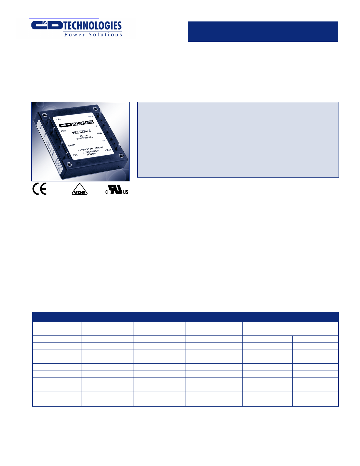
60 Watt Single Output Half Brick DC/DC Converter
The VKA60xS Series DC/DC
converters present an economical and
practical solution for distributed
power system architectures which
require high power density and
efficiency while maintaining system
modularity and upgradeability. With
the ability to operate over a wide
input voltage range of 18 to 36 and
33 to 75 volts, these modules are
18-36 V & 33 - 75V Input Range
High Efficiency: 87% Typical at
5V
100µS Transient Response 50-
100% Load Step
420 kHz Fixed-Frequency
Operation
Remote Sense
ideal for use in battery backup
applications common in todays'
telecommunication and electronic
data processing applications. The
output is fully isolated from the
input, allowing for a variety of
polarity and grounding configurations.
The VKA60xS's proprietary
control circuitry responds to 50-100%
Operation to +100°C Baseplate
Temperature
Primary Remote On/Off, Choice of
Pos/Neg Logic
Adjustable Output Voltage
Continuout Short-Circuit Protection
Thermal Shutdown
Case Ground Pin
load steps in 100µSeconds to within
1% nominal Vout.
The patented fixed frequency
architecture combined with surface
mount technology results in a compact, efficient and reliable solution to
DC/DC conversion requirements.
Safety per UL1950, EN 60950 and
CSA 22.2 #234
PRODUCT SELECTION CHART
MODEL INPUT VOUT IOUT EFFICIENCY
VKA60LS03 3.3V 12.0 80 81
VKA60LS05 24VDC 5.0V 12.0 85 86
VKA60LS12 12.0V 5.0 87 88
VKA60LS15 (18-36) 15.0V 4.0 88 89
VKA60LS24 24.0V 2.5 89 90
VKA60MS03 3.3V 12.0 81 82
VKA60MS05 48VDC 5.0V 12.0 86 87
VKA60MS12 12.0V 5.0 88 89
VKA60MS15 (33-75) 15.0V 4.0 89 90
VKA60MS24 24.0V 2.5 89 90
VOLTAGE (VDC) (A) MIN TYP
Page 2

SPECIFICATIONS, ALL MODELS
Specifications are at T
PARAMETER CONDITIONS MIN TYP MAX UNITS
INPUT
Voltage Range
VKA60LS 18 24 36 VDC
VKA60MS 33 48 75 VDC
Maximum Input Current
VKA60LS VIN = 16VDC 4.4 A
VKA60MS VIN = 27VDC 2.6 A
Reflected Ripple Current Peak - Peak 20 mA
Input Ripple Rejection DC to 1KHz 50 60 dB
No Load Input Current LS/MS 50/100 mA
Power Dissipation LS/MS
INPUT
No Load 3.6/4.8 W
Standby, Primary On/Off Disabled LS/MS 0.18/0.4 W
Inrush Charge VIN = VINmax.
VKA60LS 0.520 mC
VKA60MS 0.360 mC
Quiescent Operating Current
Primary On/Off Disabled 8 12 mA
PARAMETER CONDITIONS MIN TYP MAX UNITS
OUTPUT
Rated Power 0 60 W
Set point Accuracy 1%
Line Regulation High Line to Low Line 0.02 0.05 %
Load Regulation No Load to Rated Load 0.02 0.05 %
Output Temperature Drift ±.02 %/°C
Output Ripple, p-p DC to 20MHz BW 1% V
Output Current Limit Inception 130% l
Output Short-Circuit Current (2) test 110% l
OUTPUT
Output Overvoltage Limit 125% 135% V
Transient Response 50 to 100% Load Step
Peak Deviation di/dt = 1.0A/µSec 2% V
Settling Time V
PARAMETER CONDITIONS MIN TYP MAX UNITS
ISOLATION
Input to Output Peak Test for 2 Seconds 1500 VDC
Input to Baseplate 1500 VDC
Output to Baseplate 500 VDC
Resistance 10 MΩ
Capacitance 2000 pF
Leakage Current V
GENERAL
Efficiency, Line, Load, Temp. (3)
Switching Frequency 400 420 440 KHz
Remote Sense Compensation 0.5 V
Output Voltage Adjust Range 12V & higher(4) -50% / +25% V
Remote On/Off Control Inputs
Primary Open Collector/Drain
Sink Current-Logic Low 1.0 mA
GENERAL
Vlow 0.4 V
Vhigh Open Collector
Turn-on Time Within 1% of Rated Output 10.0 12.5 mSec
Weight 85 (3.0) g (oz.)
TEMPERATURE
Operation/Specification Case Temperature -40 +25 +100 °C
Storage Case Temperature -55 +25 +125 °C
Shutdown Temperature Case Temperature +100 +115 °C
Thermal Impedance, case-ambient 7.1 °C/W
Lead Solder Temperature 10 Seconds max +300 °C
NOTES: (1) See Typical Performance Curves, page 3
Product: www.cdpowerelectronics.com
(2) Continuous Mode
(3) See graphs for Efficiency vs. Output Load, VIN, T
(4) 3.3V Models Limited in Trim Down Range
(5) Consult Factory for Details
= +40°C nominal input voltage unless otherwise specified.
CASE
, 1% of Nominal Output 100 µSec
OUT
= 240VAC, 60Hz 180 µA, rms
ISO
CASE
VKA60xS Rev C 3/2001
OUT
OUT
OUT
OUT
OUT
, Nom
, Nom
, Nom
, Nom
, Nom
2
Page 3
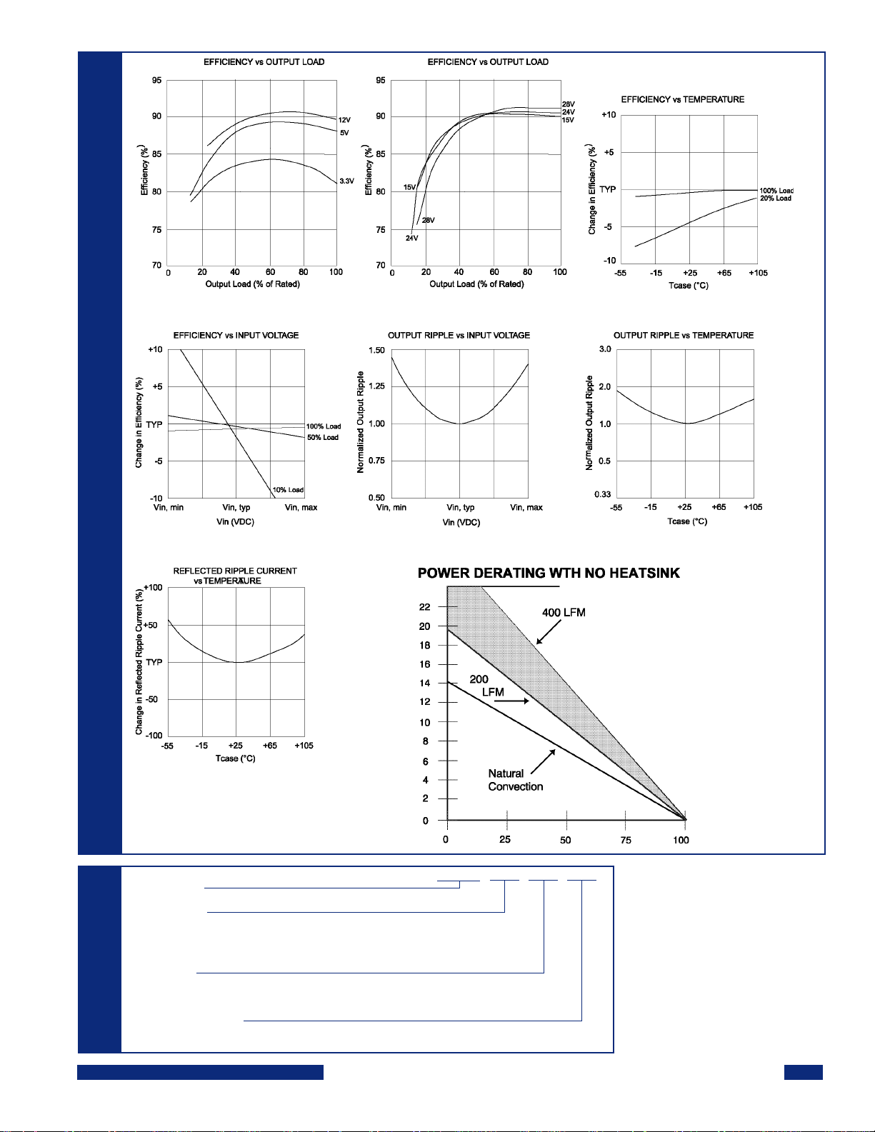
TYPICAL PERFORMANCE CURVES
= +40°C nominal input voltage unless otherwise specified.
CASE
T
Device Family
Indicates 60 Watt Regulated Unit
Model Number
Selected from Table of Electrical Characteristics
Where:
x = Input Voltage (L = 24VDC; M = 48VDC)
zz = Output Voltage (03=3.3V, 05=5V, etc.)
Lead Length
ORDERING
Product: www.cdpowerelectronics.com
0.200" - No Number
0.145" - (6)
0.110" - (8)
INFORMATION
Remote On-Off Logic:
Positive - No Number
Negative - (1)
VKA60 xSzz -
VKA60xS Rev C 3/2001
3
Page 4
0.530 MAX
[13.46]
0.20 [5.1]
0.20 [5.1]
0.50 [12.7]
.040 [1.02] DIA.
7 PLACES
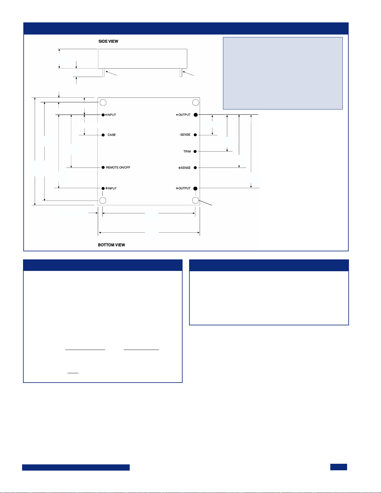
MECHANICAL
.081 [2.06] DIA.
2 PLACES
NOTES:
All dimensions are in inches (millimeters).
PIN PLACEMENT TOLERANCE: ± 0.005"
MECHANICAL TOLERANCE: ± 0.015"
Marked with: specific modeL ordered, date code, job code.
MATERIAL: Units are encapsulated in a low thermal
resistance molding compound which has excellent chemical
resistance and electrical properties in high humidity
environments and over a wide operating temperature range.
The encapsulant and outer shell of the unit have UL94V-0
ratings. Lead material is solder plated to allow ease of
solderability.
0.40 [10.16]
2.000
2.40
[61.0]
MAX
[50.80]
1.400
[35.56]
1.000
[25.40]
0.19 [4.8]
VKA60xS
1.900
[48.26]
2.28
[57.91]
MAX
OUTPUT ADJUST VOLTAGE
This feature allows the user to accurately adjust the
module's output voltage set point to a specified level.
This is achieved by connecting a resistor or potentiometer
from the TRIM terminal to either the +Vout terminal (for
increased Vout) or the -Vout terminal (for decreased
Vout). The formulae below describe the trim resistor
value to obtain a Vout change of ∆%. VO is output
voltage prior to adjustment (3.3V, 5V, 12V, 15V, or 24V).
.400 [10.16]
0.700
[17.78]
1.000
[25.40]
1.400
[35.56]
MOUNTING INSERTS M3 X 0.5 THRU, 4 PLACES
MAX. TORQUE, 8 IN/LBS
OVP NOTE
Special attention should be given to the peak voltage
deviation during a dynamic load step when trimming
the output above the original set point to avoid
tripping the overvoltage protection circuit. Should an
OVP condition occur, the converter will go into a
latch condition and must be externally reset before it
will return to normal operation.
Radj - up = (
Vo(100 + ∆%)
1.225∆% ∆%
Radj - down = (
C&D Technologies (Power Electronics) Ltd.
Shannon, Co. Clare, Ireland
Tel: +353.61.474.133 Fax:+353.61.474.141
Any data, prices, descriptions or specifications presented herein are subject to revision by C&D Technologies, Inc. without notice. While such information is believed to be
accurate as indicated herein, C&D Technologies, Inc. makes no warranty and hereby disclaims all warranties, express or implied, with regard to the accuracy or
completeness of such information. Further, because the product(s) featured herein may be used under conditions beyond its control, C&D Technologies, Inc. hereby
disclaims all warranties, either express or implied, concerning the fitness or suitability of such product(s) for any particular use or in any specific application or arising from
any course of dealing or usage of trade. The user is solely responsible for determining the suitability of the product(s) featured herein for user’s intended purpose and in
user’s specific application. C&D Technologies, Inc. does not warrant or recommend that any of its products be used in any life support or aviation or aerospace applications.
Product: www.cdpowerelectronics.com
100
∆%
- 2)
kΩ
_
(100 + 2∆%)
3400 E Britannia Drive, Tucson, Arizona 85706
kΩ
)
Power Electronics Division, United States
Tel: 800.547.2537 Fax: 520.770.9369
VKA60xS Rev C 3/2001
C&D Technologies, (NCL)
Tel: +44 (0)1908 615232 Fax: +44 (0)1908 617545
Milton Keynes MK14 5BU UK
4
 Loading...