

现货库存、技术资料、百科信息、热点资讯,精彩尽在鼎好!
Features
VIPER28
Off-line high voltage converters
■ 800 V avalanche rugged power section
■ PWM operation with frequency jittering for low
EMI
■ Operating frequency:
– 60 kHz for L type
– 115 kHz for H type
■ Standby power < 50 mW at 265 Vac
■ Limiting current with adjustable set point
■ Adjustable and accurate over-voltage
protection
■ On-board soft-start
■ Safe auto-restart after a fault condition
■ Hysteretic thermal shutdown
■ Delayed overload protection
Application
■ Auxiliary power supply for consumer and home
equipment
■ ATX auxiliary power supply
■ Low / medium power AC-DC adapters
■ SMPS for set-top boxes, DVD players and
recorders, white goods
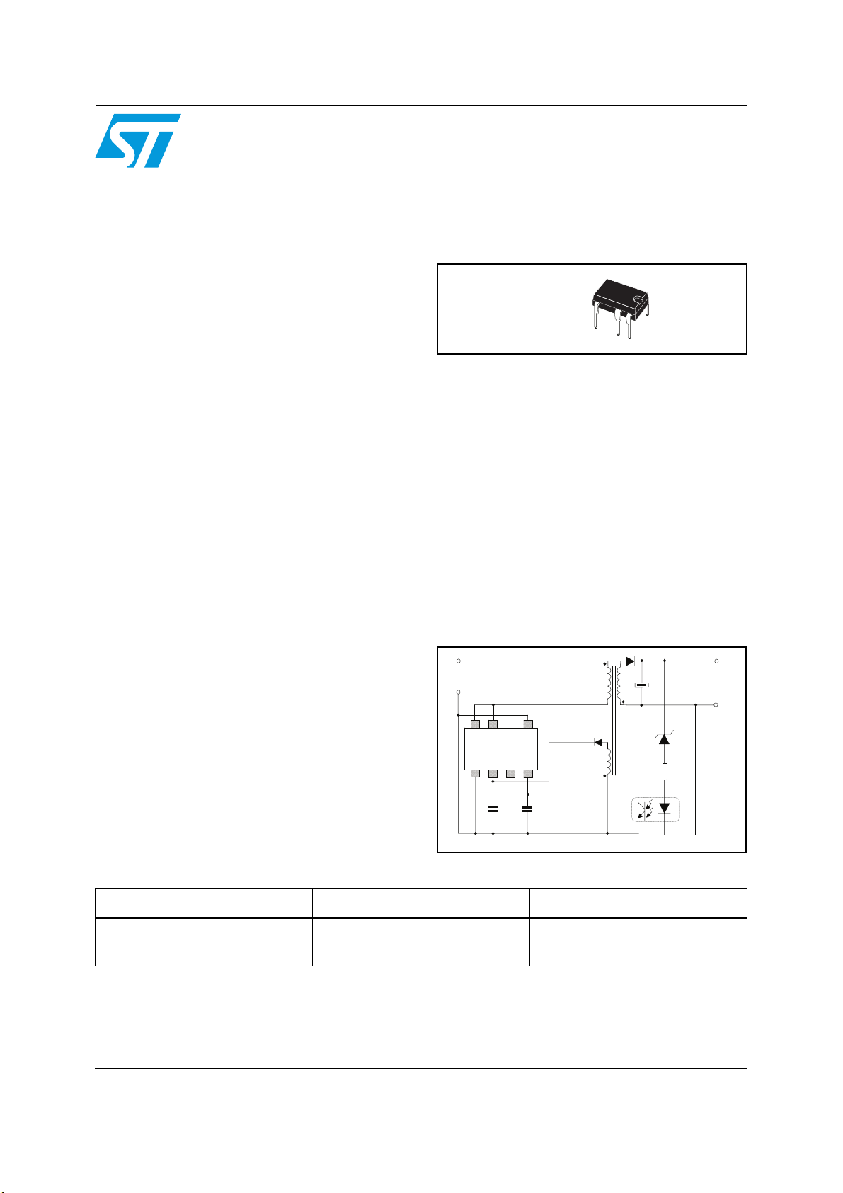
DIP-7DIP-7
Description
The device is an off-line converter with an 800 V
rugged power section, a PWM control, two levels
of over-current protection, over-voltage and
overload protections, hysteretic thermal
protection, soft-start and safe auto-restart after
any fault condition removal. Burst mode operation
and device very low consumption helps to meet
the standby energy saving regulations. Advance
frequency jittering reduces EMI filter cost. The
extra power timer allows the management of
output peak power for a designed time window.
The high voltage start-up circuit is embedded in
the device.
Figure 1. Typical topology
+
DC input high voltage
wide range
-
DRAIN
DRAIN
VIPER28
VDD
GND
CONT
EPT
FB
+
DC Output voltage
-
Table 1. Device summary
Order codes Package Packaging
VIPER28LN
DIP-7 Tube
VIPER28HN
September 2008 Rev 1 1/29
www.st.com
29

Contents VIPER28
Contents
1 Block diagram . . . . . . . . . . . . . . . . . . . . . . . . . . . . . . . . . . . . . . . . . . . . . . 4
2 Typical power . . . . . . . . . . . . . . . . . . . . . . . . . . . . . . . . . . . . . . . . . . . . . . . 4
3 Pin settings . . . . . . . . . . . . . . . . . . . . . . . . . . . . . . . . . . . . . . . . . . . . . . . . 5
3.1 Connection diagram . . . . . . . . . . . . . . . . . . . . . . . . . . . . . . . . . . . . . . . . . . 5
3.2 Pin description . . . . . . . . . . . . . . . . . . . . . . . . . . . . . . . . . . . . . . . . . . . . . . 5
4 Electrical data . . . . . . . . . . . . . . . . . . . . . . . . . . . . . . . . . . . . . . . . . . . . . . 6
4.1 Maximum ratings . . . . . . . . . . . . . . . . . . . . . . . . . . . . . . . . . . . . . . . . . . . . 6
4.2 Thermal data . . . . . . . . . . . . . . . . . . . . . . . . . . . . . . . . . . . . . . . . . . . . . . . 6
4.3 Electrical characteristics . . . . . . . . . . . . . . . . . . . . . . . . . . . . . . . . . . . . . . . 7
5 Typical electrical characteristics . . . . . . . . . . . . . . . . . . . . . . . . . . . . . . 11
6 Typical circuit . . . . . . . . . . . . . . . . . . . . . . . . . . . . . . . . . . . . . . . . . . . . . 14
7 Operation descriptions . . . . . . . . . . . . . . . . . . . . . . . . . . . . . . . . . . . . . . 15
7.1 Power section and gate driver . . . . . . . . . . . . . . . . . . . . . . . . . . . . . . . . . 15
7.2 High voltage startup generator . . . . . . . . . . . . . . . . . . . . . . . . . . . . . . . . . 15
7.3 Power-up and soft-start up . . . . . . . . . . . . . . . . . . . . . . . . . . . . . . . . . . . . 16
7.4 Power down operation . . . . . . . . . . . . . . . . . . . . . . . . . . . . . . . . . . . . . . . 18
7.5 Auto restart operation . . . . . . . . . . . . . . . . . . . . . . . . . . . . . . . . . . . . . . . . 18
7.6 Oscillator . . . . . . . . . . . . . . . . . . . . . . . . . . . . . . . . . . . . . . . . . . . . . . . . . 18
7.7 Current mode conversion with adjustable current limit set point . . . . . . . 19
7.8 Over-voltage protection (OVP) . . . . . . . . . . . . . . . . . . . . . . . . . . . . . . . . . 19
7.9 About CONT pin . . . . . . . . . . . . . . . . . . . . . . . . . . . . . . . . . . . . . . . . . . . . 21
7.10 Feed-back and overload protection (OLP) . . . . . . . . . . . . . . . . . . . . . . . . 21
7.11 Burst-mode operation at no load or very light load . . . . . . . . . . . . . . . . . . 24
7.12 Extra power management function (EPT) . . . . . . . . . . . . . . . . . . . . . . . . 24
7.13 2nd level over-current protection and hiccup mode . . . . . . . . . . . . . . . . . 25
2/29

VIPER28 Contents
8 Package mechanical data . . . . . . . . . . . . . . . . . . . . . . . . . . . . . . . . . . . . 26
9 Revision history . . . . . . . . . . . . . . . . . . . . . . . . . . . . . . . . . . . . . . . . . . . 28
3/29
Block diagram VIPER28
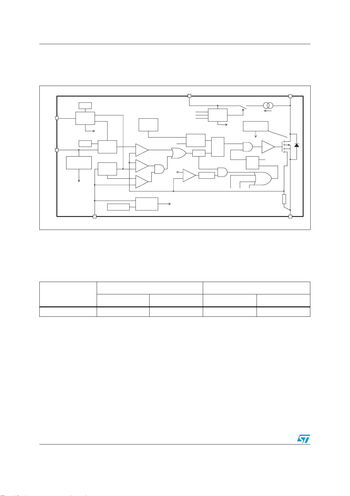
1 Block diagram
Figure 2. Block diagram
EPT
CONT
CONT
Tovl
Tovl
LEB
LEB
EPT
Tov l
Tov l
BLOCK
BLOCK
SOFT
SOFT
START
START
OVP DETECTION
OVP DETECTION
LOGIC
LOGIC
OVP
OVP
OLP
OLP
OCP
OCP
BLOCK
BLOCK
PWM
PWM
BLOCK
BLOCK
BURST-MODE
BURST-MODE
REFERENCES
REFERENCES
OSCI LLATOR
OSCI LLATOR
-
-
OCP
OCP
+
+
PWM
PWM
+
+
-
-
+
+
-
Disable
Disable
BURST-MODE
BURST-MODE
LOGIC
LOGIC
BURST
BURST
Vcc
VDD
Internal Supply bus
Internal Supply bus
&
&
Ref erence Voltag es
Ref erence Voltag es
TURN-ON
TURN-ON
2nd OCP
2nd OCP
-
-
+
+
BURST
BURST
LOGIC
LOGIC
LEB
LEB
2nd OCP
2nd OCP
LOGIC
LOGIC
SUPPLY
SUPPLY
& UVLO
& UVLO
S
S
R
R
UVLO
UVLO
Q
Q
OTP OVP OLP
OTP OVP OLP
HV_ON Ist art-up
HV_ON Ist art-up
TH ER MAL
TH ER MAL
SHUTD OWN
SHUTD OWN
OTP
OTP
HV_ON
HV_ON
SRQ
SRQ
Rsense
Rsense
DRAIN
DRAIN
FB
FB
2 Typical power
Table 2. Typical power
Part number
1. Typical continuous power in non ventilated enclosed adapter measured at 50 °C ambient.
2. Maximum practical continuous power in an open frame design at 50
Adapter
(1)
230 V
AC
Open frame
(2)
Adapter
85-265 V
(1)
VIPER28 18 W 24 W 10 W 13 W
°C ambient, with adequate heat sinking.
GND
GND
AC
Open frame
(2)
4/29
VIPER28 Pin settings
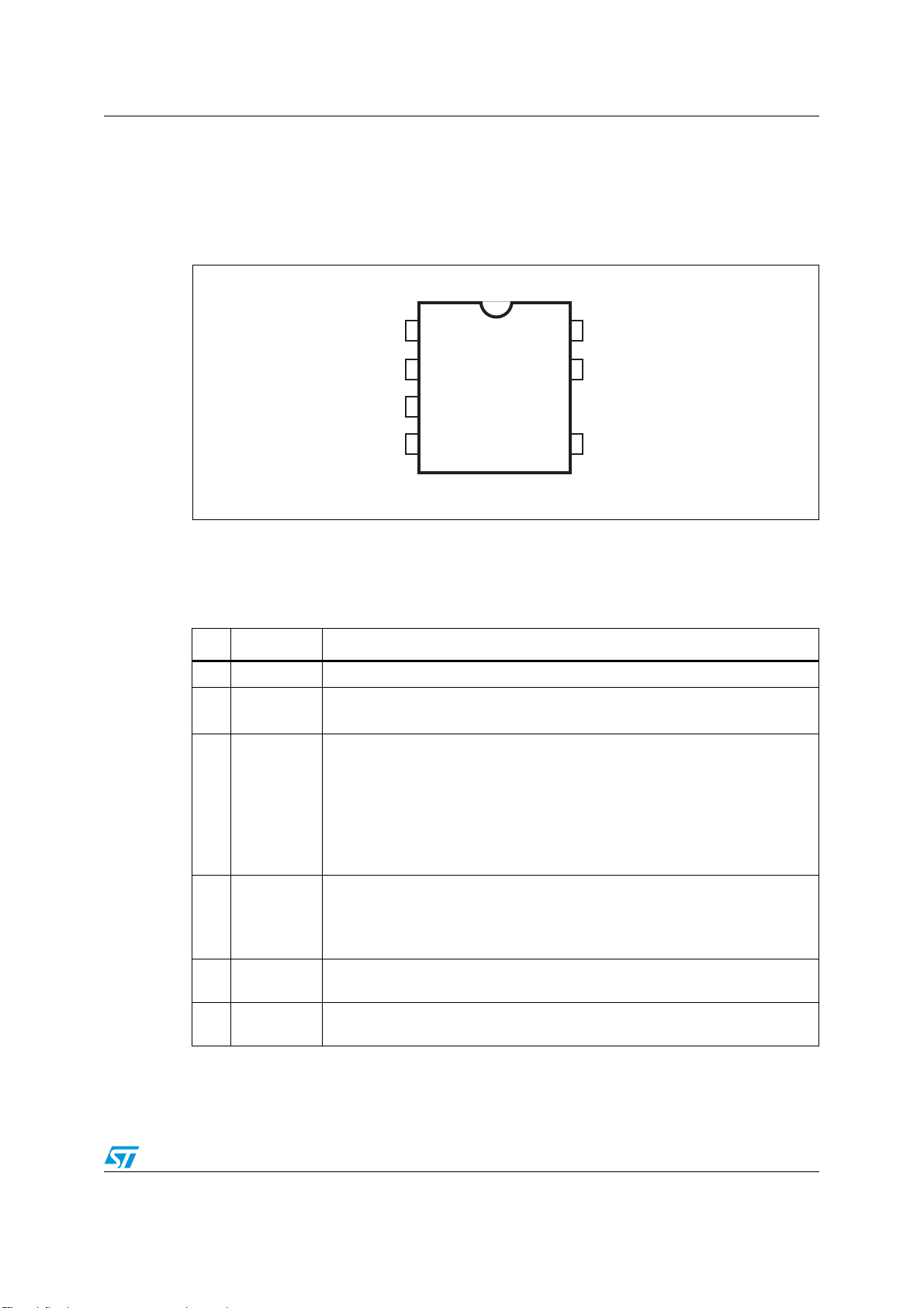
3 Pin settings
3.1 Connection diagram
Figure 3. Connection diagram (top view)
3.2 Pin description
Table 3. Pin description
N. Name Function
1 GND This pin represents the device ground and the source of the power section.
2VDD
3CONT
4FB
5 EPT
7,8 DRAIN
Supply voltage of the control section. This pin also provides the charging
current of the external capacitor during start-up time.
Control pin. The following functions can be selected:
1. current limit set point adjustment. The internal set default value of the cycleby-cycle current limit can be reduced by connecting to ground an external
resistor.
2. output voltage monitoring. A voltage exceeding 3 V shuts the IC down
reducing the device consumption. This function is strobed and digitally filtered
for high noise immunity.
Control input for duty cycle control. Internal current generator provides bias
current for loop regulation. A voltage below 0.6 V activates the burst-mode
operation. A level close to 3.3 V means that the device is approaching the
cycle-by-cycle over-current set point.
This pin allows the connection of an external capacitor for the extra power
management. If the function is not used, the pin has to be connected to GND.
High voltage drain pin. The built-in high voltage switched start-up bias current is
drawn from this pin too.
GND
VDD
CONT
FB
DRAIN
DRAIN
EPT
BR
5/29
Electrical data VIPER28
4 Electrical data
4.1 Maximum ratings
Table 4. Absolute maximum ratings
Symbol Pin Parameter Value Unit
V
DRAIN
E
I
AR
I
DRAIN
V
CONT
V
V
EPT
V
I
DD
P
TOT
T
T
STG
AV
FB
DD
J
7, 8 Drain-to-source (ground) voltage 800 V
7, 8 Repetitive avalanche energy (limited by TJ = 150 °C) 5 mJ
7, 8 Repetitive avalanche current (limited by TJ = 150 °C) 1.5 A
7, 8 Pulse drain current 3 A
3 Control input pin voltage (with I
4 Feed-back voltage -0.3 to 5.5 V
5 EPT input pin voltage 5 V
2 Supply voltage (IDD = 25 mA) Self limited V
2 Input current 25 mA
4.2 Thermal data
Table 5. Thermal data
Symbol Parameter Max value Unit
= 1 mA) Self limited V
CONT
Power dissipation at TA < 50 °C 1 W
Operating junction temperature range -40 to 150 °C
Storage temperature -55 to 150 °C
R
R
1. When mounted on a standard single side FR4 board with 100 mm2 (0.155 sq in) of Cu (35 m thick)
Thermal resistance junction pin 25 °C/W
thJP
Thermal resistance junction ambient 75
thJA
6/29
(1)
°C/W
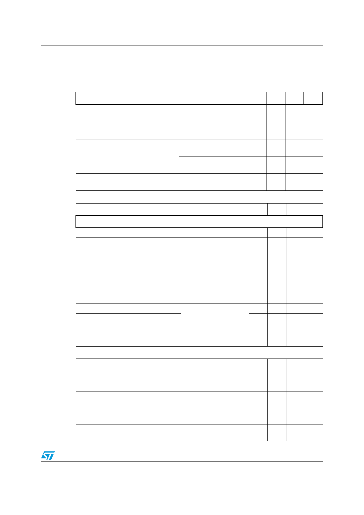
VIPER28 Electrical data
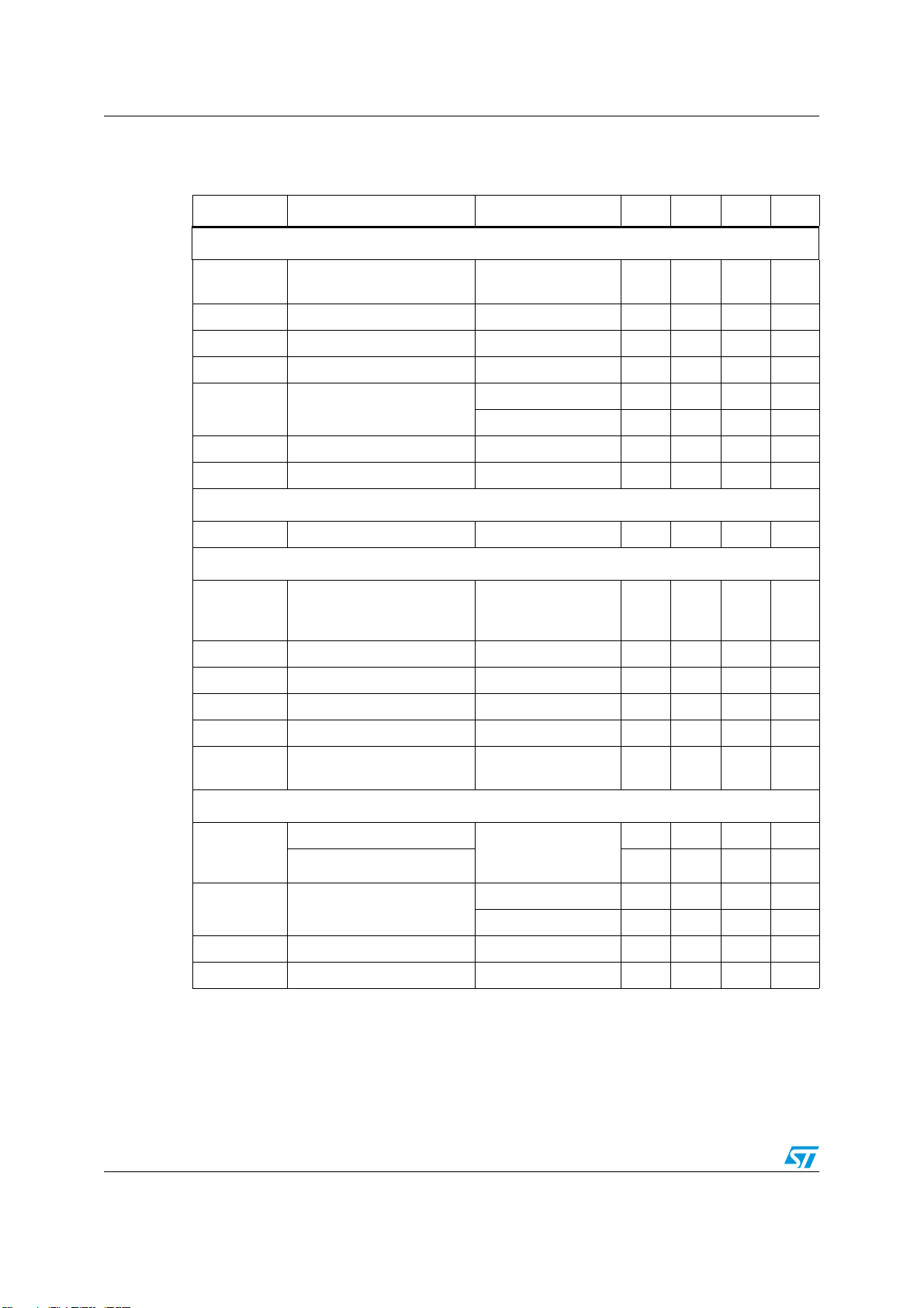
4.3 Electrical characteristics
(TJ = -25 to 125 °C, VDD = 14 V; unless otherwise specified)
Table 6. Power section
Symbol Parameter Test condition Min Typ Max Unit
I
= 1 mA, VFB = GND
V
BVDSS
I
OFF
R
DS(on)
C
OSS
Table 7. Supply section
Break-down voltage
OFF state drain current
Drain-source on state
resistance
Effective (energy related)
output capacitance
Symbol Parameter Test condition Min Typ Max Unit
DRAIN
TJ = 25 °C
V
V
I
V
I
V
V
= max rating,
DRAIN
= GND
FB
= 0.4 A, VFB = 3 V,
DRAIN
= GND, TJ = 25 °C
EPT
= 0.4 A, VFB = 3 V,
DRAIN
= GND, TJ = 125 °C
EPT
= 0 to 640 V 40 pF
DRAIN
800 V
60 μA
7 Ω
14 Ω
Volt ag e
V
DRAIN
I
DDch
V
DD
V
DDclamp
V
DDon
V
DDoff
V
DD(RESTART)
Current
I
DD0
I
DD1
I
DD_FAULT
I
DD_OFF
Drain-source start voltage 60 80 100 V
_START
Start up charging current
V
V
V
V
V
= 120 V,
DRAIN
= GND, VFB = GND,
EPT
= 4 V
DD
= 120 V,
DRAIN
= GND, VFB = GND,
EPT
-2 -3 -4 mA
-0.4 -0.6 -0.8 mA
VDD = 4 V after fault.
Operating voltage range After turn-on 8.5 23.5 V
VDD clamp voltage IDD = 20 mA 23.5 V
VDD start up threshold
VDD under voltage
shutdown threshold
VDD restart voltage
threshold
Operating supply current,
not switching
Operating supply current,
switching
V
V
V
V
= 120 V,
DRAIN
= GND, VFB = GND
EPT
= 120 V,
DRAIN
= GND, VFB = GND
EPT
VFB = GND, FSW = 0 k H z ,
V
= GND, VDD = 10 V
EPT
V
DRAIN
= 120 V,
FSW = 60 kHz
V
DRAIN
= 120 V,
13 14 15 V
7.588.5V
44.55 V
FSW = 115 kHz
Operating supply current,
with protection tripping
Operating supply current
with VDD < V
DD_OFF
VDD = 7 V 270 uA
0.9 mA
2.5 mA
3.5 mA
400 uA
7/29
Electrical data VIPER28
Table 8. Controller section
(T
= -25 to 125 °C, V
J
Symbol Parameter Test condition Min Typ Max Unit
Feed-back pin
= 14 V; unless otherwise specified)
DD
V
FBolp
V
FBlin
V
FBbm
V
FBbmhys
Over-load shut down
threshold
Linear dynamics upper limit 3.2 3.5 3.7 V
Burst mode threshold Voltage falling 0.6 V
Burst mode hysteresis Voltage rising 100 mV
4.7 4.8 5.2 V
VFB = 0.3 V -150 -200 -280 uA
I
R
FB(DYN)
H
FB
FB
Feed-back sourced current
Dynamic resistance V
ΔVFB / ΔI
D
3.3 V < V
FB
< 4.8 V -3 uA
FB
< 3.3 V 14 20 kΩ
26V/A
CONT pin
VCONT_l Low level clamp voltage I
= -100 uA 0.5 V
CONT
Current limitation
VFB = 4 V,
I
Dlim
Max drain current limitation
I
CONT
= -10 µA
0.75 0.80 0.85 A
TJ = 25 °C
t
SS
T
ON_MIN
Soft-start time 8.5 ms
Minimum turn ON time 220 400 480 ns
td Propagation delay 100 ns
t
LEB
I
D_BM
Leading edge blanking 300 ns
Peak drain current during
burst mode
Oscillator section
VIPER28LV
F
OSC
FD Modulation depth
FM Modulation frequency 250 Hz
D
MAX
8/29
VIPER28H 103 115 127 kHz
Maximum duty cycle 70 80 %
V
= 0.6 V 160 mA
FB
= operating
DD
54 60 66 kHz
voltage range,
VFB = 1 V
VIPER28L±4kHz
VIPER28H ±8 kHz
VIPER28 Electrical data
Table 8. Controller section (continued)
(T
= -25 to 125 °C, V
J
Symbol Parameter Test condition Min Typ Max Unit
= 14 V; unless otherwise specified)
DD
Over-current protection (2
I
DMAX
Second over-current
threshold
Over-voltage protection
V
OVP
T
STROBE
Over-voltage protection
threshold
Over-voltage protection
strobe time
Extra power management
I
DLIM_EPT
V
EPT(STOP)
V
EPT(RESTART)
I
EPT
Drain current limit with
EPT function
EPT shut down threshold
EPT restart threshold 0.6 V
Sourced EPT current 5 μA
Thermal shutdown
T
T
HYST
SD
Thermal shutdown
temperature
Thermal shutdown
hysteresis
nd
OCP)
I
CONT
T
I
CONT
< -10 μA
= 25 °C
J
< -10 μA
1.2 A
2.733.3V
2.2 us
85%
IDLIM
A
4V
150 170 °C
30 °C
9/29

Electrical data VIPER28
Figure 4. Minimum turn-on time test circuit
EPT
Figure 5. OVP threshold test circuits
EPT
(The OVP protection is triggered
after four consecutive oscillator cycles)
10/29

VIPER28 Typical electrical characteristics
5 Typical electrical characteristics
Figure 6. Current limit vs TJ Figure 7. Switching frequency vs T
J
Figure 8. Drain start-up voltage vs T
J
Figure 10. Operating supply current
(no switching) vs T
J
Figure 9. HFB vs T
J
Figure 11. Operating supply current
(switching) vs T
J
11/29

Typical electrical characteristics VIPER28
Figure 12. current limit vs R
Figure 13. Power MOSFET on-resistance
LIM
Figure 14. Power MOSFET break down
voltage vs T
J
vs T
J
12/29

VIPER28 Typical electrical characteristics
Figure 15. Thermal shutdown
T
J
TSD
T
HYST
V
V
DD RESTART
V
DD OFF
DD ON
V
DD
V
DS
t
t
t
13/29

Typical circuit VIPER28
6 Typical circuit
Figure 16. Flyback application (basic)
EPT
Figure 17. Flyback application
EPT
14/29

VIPER28 Operation descriptions
7 Operation descriptions
VIPER28 is a high-performance low-voltage PWM controller chip with an 800 V, avalanche
rugged Power section.
The controller includes: the oscillator with jittering feature, the start up circuits with soft-start
feature, the PWM logic, the current limit circuit with adjustable set point, the second
over-current circuit, the burst mode management circuit, the EPT circuit, the UVLO circuit,
the auto-restart circuit and the thermal protection circuit.
The current limit set-point is set by the CONT pin. The burst mode operation guaranties high
performance in the stand-by mode and helps in the energy saving norm accomplishment.
All the fault protections are built in Auto Restart Mode with very low repetition rate to prevent
IC's overheating.
7.1 Power section and gate driver
The Power section is implemented with an avalanche ruggedness N-channel MOSFET,
which guarantees safe operation within the specified energy rating as well as high dv/dt
capability. The Power section has a BV
at 25 °C.
of 800 V min. and a typical R
DSS
DS(on)
of 7 Ω
The integrated SenseFET structure allows a virtually loss-less current sensing.
The gate driver is designed to supply a controlled gate current during both turn-on and turnoff in order to minimize common mode EMI. Under UVLO conditions an internal pull-down
circuit holds the gate low in order to ensure that the Power section cannot be turned on
accidentally.
7.2 High voltage startup generator
The HV current generator is supplied through the DRAIN pin and it is enabled only if the
input bulk capacitor voltage is higher than V
the HV current generator is ON, the
capacitor on the V
pin. In case of Auto Restart mode after a fault event, the I
DD
I
DDch
is reduced to 0.6 mA, typ. in order to have a slow duty cycle during the restart phase.
See Figure 18 on page 16.
DRAIN_START
current (3 mA typical value) is delivered to the
threshold, 80 VDC typically. When
current
DDch
15/29

Operation descriptions VIPER28
7.3 Power-up and soft-start up
If the input voltage rises up till the device start level (V
to grow due to the
voltage start up circuit. If the V
I
current (see Table 6 on page 7) coming from the internal high
DDch
voltage reaches V
DD
DRAIN_START
threshold (~14 V) the power
DDon
), the VDD voltage begins
MOSFET starts switching and the HV current generator is turned OFF. See Figure 19 on
page 17.
The IC is powered by the energy stored in the capacitor on the VDD Pin, C
, until the self-
VDD
supply circuit (typically an auxiliary winding of the transformer and a steering diode)
develops a voltage high enough to sustain the operation.
C
capacitor must be sized enough to avoid fast discharge and keep the needed voltage
VDD
value higher than V
threshold: a too low capacitance value could terminate the
DDoff
switching operation before the controller receives any energy from the auxiliary winding.
The following formula can be used for the V
capacitor calculation:
DD
Equation 1
I
×
DDchtSSaux
VDD
----------------------------------------=
V
–
DDonVDDoff
The t
C
is the time needed for the steady state of the auxiliary voltage. This time is
SSaux
estimated by applicator according to the output stage configurations (transformer, output
capacitances, etc.).
During the converter start up time, the drain current limitation is progressively increased to
the maximum value. In this way the stress on the secondary diode is considerably reduced.
It also helps to prevent transformer saturation. The soft-start time lasts 8.5 ms and the
feature is implemented for every attempt of start up converter or after a fault. See Figure 20
on page 17.
Figure 18. Start up I
I
DD
2 mA
1 mA
I
DD_FAULT
I
DD_OFF
I
DS_CH_FAULT
-1 mA
-2 mA
-3 mA
-4 mA
I
I
DS_CH
DD0
V
DD
DDrestart
current
V
DDoff
16/29
V
= 120V
DS
= 0 kHz
F
SW
AFTER FAULT
V
DDon
VDD

VIPER28 Operation descriptions
V
V
V
Figure 19. Timing diagram: normal power-up and power-down sequences
Vin
Vin
Start
Start
V
V
V
V
V
Vcc
Vcc
V
DD
Vcc
Vcc
DRAIN
I
DDch
I
I
3 mA
3 mA
DD
cc
cc
DD
Vcc
Vcc
DD
OFF
OFF
restart
restart
charge
charge
ON
ON
Power
Power
Normal
-
-
on
on
Normal
operation
operation
regulation is lost here
regulation is lost here
Power - off
Power - off
t
t
t
t
t
t
t
t
t
t
t
t
Figure 20. Soft-start: timing diagram
I
DRAIN
t
ss
IDLIM
V
FB
V
FB OL P
V
FB_lin
t
t
17/29

Operation descriptions VIPER28
7.4 Power down operation
At converter power down, the system loses regulation as soon as the input voltage is so low
that the peak current limitation is reached. The V
the V
the IC is interrupted and consequently the V
on page 17. Later, if the V
threshold (8 V typical) the power MOSFET is switched OFF, the energy transfer to
DDoff
is lower than V
IN
DD
DRAIN_START
voltage drops and when it falls below
DD
voltage continues to decreases, Figure 19
(80 V typical), the start up sequence
is inhibited and the power down completed. This feature is useful to prevent converter’s
restart attempts and ensures monotonic output voltage decay during the system power
down.
7.5 Auto restart operation
If after a converter power down, the VIN is higher than V
is not inhibited and will be activated only when the V
DRAIN_START,
voltage drops down the V
DD
threshold (4.5 V typical). This means that the HV start up current generator restarts the V
capacitor charging only when the V
voltage drops below V
DD
DDrestart
the start up sequence
DDrestart
DD
. The scenario above
described is for instance a power down because of a fault condition. After a fault condition,
the charging current is 0.6 mA (typ.) instead of the 3 mA (typ.) of a normal start up converter
phase. This feature together with the low V
DDrestart
threshold (4.5 V) ensures that, after a
fault, the restart attempts of the IC has a very long repetition rate and the converter works
safely with extremely low power throughput. The Figure 21 shows the IC behavioral after a
short circuit event.
Figure 21. Timing diagram: behavior after short circuit
V
V
DD
DD
V
V
DD
DDon
V
V
DD
DDoff
V
DD(RESTART)
VDS
VDS
IDD_CH
IDD_CH
0.6 mA
0.6 mA
Short circuit occurs here
Short circuit occurs here
Trep
Trep
< 0.03Trep
< 0.03Trep
t
t
t
t
t
t
FB Pin
FB Pin
4.8 V
4.8 V
3.3 V
3.3 V
7.6 Oscillator
The switching frequency is internally fixed to 60 kHz or 115 kHz. In both case the switching
frequency is modulated by approximately ±4 kHz (60 kHz version) or ±8 kHz
(115 kHz version) at 250 Hz (typical) rate, so that the resulting spread-spectrum action
distributes the energy of each harmonic of the switching frequency over a number of sideband harmonics having the same energy on the whole but smaller amplitudes.
18/29
t
t
t
t

VIPER28 Operation descriptions
7.7 Current mode conversion with adjustable current limit set
point
The device is a current mode converter: the drain current is sensed and converted in voltage
that is applied to the non inverting pin of the PWM comparator. This voltage is compared
with the one on the feed-back pin through a voltage divider on cycle by cycle basis.
The VIPER28 has a default current limit value, I
the electrical specification, by the R
resistor connected to the CONT see Figure 12 on
LIM
page 12.
The CONT pin has a minimum current sunk needed to activate the I
R
or with high R
LIM
(i.e. 100 kΩ) the current limit is fixed to the default value (see I
LIM
Table 8 on page 8).
7.8 Over-voltage protection (OVP)
The device can monitor the converter output voltage. This operation is done by CONT pin
during power MOSFET OFF-time, when the voltage generated by the auxiliary winding
tracks converter's output voltage, through turn ratio See Figure 22.
In order to perform the output voltage monitor, the CONT pin has to be connected to the aux
winding through a resistor divider made up by R
(see Figure 17 (R3, R4 are respectively R
applied to the CONT pin exceeds the internal 3 V reference for four consecutive times the
controller recognizes an over-voltage condition. This special feature uses an internal
counter; that is to reduce sensitivity to noise and prevent the latch from being erroneously
activated. see Figure 22 on page 20. The counter is reset every time the OVP signal is not
triggered in one oscillator cycle.
Referring to the Figure 17, the resistors divider ratio k
OVP
, that the designer can adjust according
DLIM
adjustment: without
DLIM
N
AUX
--------------
N
SEC
and R
LIM
and R
OVP
)and Figure 23). If the voltage
LIM
will be given by:
OVP
DLIM
,
Equation 2
Equation 3
k
OVP
V
---------------------------------------------------------------------------------------------------=
N
AUX
--------------
N
V
SEC
k
OVP
19/29
OVP
OUTOVPVDSEC
+()V
R
LIM
----------------------------------=
R
+
LIMROVP
–⋅
DAUX

Operation descriptions VIPER28
U
Where:
● V
● V
● N
● N
● V
● V
● R
Than, fixed R
is the OVP threshold (see Table 8 on page 8)
OVP
OUT OVP
AUX
SEC
DSEC
DAUX
OVP
is the converter output voltage value to activate the OVP set by designer
is the auxiliary winding turns
is the secondary winding turns
is the secondary diode forward voltage
is the Auxiliary diode forward voltage
together R
according to the desired I
LIM,
make the Output Voltage divider
LIM
DLIM
, the R
can be calculating by:
OVP
Equation 4
1k
–
OVP
R
OVP
-----------------------
R
×=
LIM
k
OVP
The resistor values will be such that the current sourced and sunk by the CONT pin be
within the rated capability of the internal clamp.
Figure 22. OVP timing diagram
V
V
DS
DS
VA
X
0
0
CONT
(pin 4)
(pin 4)
3V
3V
0.5 µs
STROBE
STROBE
OVP
OVP
COUNTER
COUNTER
RESET
RESET
COUNTER
COUNTER
STATUS
STATUS
FAULT
FAULT
2 µs
2 µs
0 0 0
0 0 0
NORMAL OPERATION TEMPORARY DISTURBANCE FEEDBACK LOOP FAILURE
NORMAL OPERATION TEMPORARY DISTURBANCE FEEDBACK LOOP FAILURE
0.5 µs
→
→
1
1
0
0
t
t
t
t
t
t
t
t
t
t
→
→
1
1
→
→
2
2
0
0
2
2
→
→
0
0
→
→
1
1
1
1
→
→
2
2
2
2
→
→
3
3
3
3
t
40
40
t
t
t
t
20/29

VIPER28 Operation descriptions
7.9 About CONT pin
Referring to the Figure 23, through the CONT PIN, the below features can be implemented:
1. Current Limit set point
2. Over-voltage protection on the converter output voltage
The Table9 on page21 referring to the Figure 23, lists the external resistance combinations
needed to activate one or plus of the CONT pin functions.
Figure 23. CONT pin configuration
OCP
Daux
Auxiliary
winding
Rovp
CONT
Rlim
SOFT
START
OVP DETECTION
LOGIC
To OVP Protect ion
Curr. Lim.
BLOCK
From SenseFET
Current Limit C omparator
-
+
To PWM Logic
Table 9. CONT pin configurations
Function / component R
I
reduction See Figure 6 No No
Dlim
OVP ≥ 80 KΩ See Equation 4 Ye s
I
reduction + OVP See Figure 6 See Equation 4 Ye s
Dlim
LIM
7.10 Feed-back and overload protection (OLP)
The VIPER28 is a current mode converter: the feedback pin controls the PWM operation,
controls the burst mode and actives the overload protection of the device. Figure 24 on
page 23 and Figure 25 show the internal current mode structure.
With the feedback pin voltage between
typical values) the drain current is sensed and converted in voltage that is applied to the non
inverting pin of the PWM comparator.
This voltage is compared with the one on the feedback pin through a voltage divider on
cycle by cycle basis. When these two voltages are equal, the PWM logic orders the switch
off of the power MOSFET. The drain current is always limited to I
In case of overload the feedback pin increases in reaction to this event and when it goes
higher than
V
the drain current is limited or to the default I
FBlin
through a resistor at the CONT pin (using the R
comparator is disabled.
V
FB_bm
and V
LIM
, (respectively 0.6 V and 3.5 V,
FBlin
, see Figure 6 on page 11); the PWM
R
OVP
value.
DLIM
value or the one imposed
DLIM
D
AUX
21/29

Operation descriptions VIPER28
At the same time an internal current generator starts to charge the feedback capacitor
(C
) and when the feedback voltage reaches the V
FB
off and the start up phase is activated with reduced value of I
threshold, the converter is turned
FBolp
charge
to 0.6 mA.
During the first start up phase of the converter, after the soft-start up time (typical value is
8.5 ms) the output voltage could force the feedback pin voltage to rise up to the
V
FBolp
threshold that switches off the converter itself.
To avoid this event, the appropriate feedback network has to be selected according to the
output load. More the network feedback fixes the compensation loop stability. The Figure 24
on page 23 and Figure 25 on page 23 show the two different feedback networks.
The time from the overload detection (VFB =
(VFB =
V
) can be calculated by CFB value (see Figure 24 on page 23 and Figure 25),
FBolp
V
) to the device shutdown
FBlin
using the formula:
Equation 5
V
–
FBolpVFBlin
T
OLP delay–
In the Figure 24, the capacitor connected to FB pin (C
C
×=
FB
----------------------------------------
3μ A
) is used as part of the circuit to
FB
compensate the feedback loop but also as element to delay the OLP shut down owing to the
time needed to charge the capacitor (see Equation 5).
After the start up time, 8.5 ms typ value, during which the feedback voltage is fixed at
V
FBlin
the output capacitor could not be at its nominal value and the controller interpreters this
situation as an overload condition. In this case, the OLP delay helps to avoid an incorrect
device shut down during the start up face.
Owing to the above considerations, the OLP delay time must be long enough to by-pass the
initial output voltage transient and check the overload condition only when the output voltage
is in steady state. The output transient time depends from the value of the output capacitor
and from the load.
When the value of the C
capacitor calculated for the loop stability is too low and cannot
FB
ensure enough OLP delay, an alternative compensation network can be used and it is
showed in Figure 25 on page 23.
,
Using this alternative compensation network, two poles (f
introduced by the capacitors C
The capacitor C
introduces a pole (f
FB
and C
FB
PFB
is usually used to compensate the high frequency zero due to the ESR (Equivalent Series
Resistor) of the output capacitance of the fly-back converter.
The mathematical expressions of these poles and zero frequency, considering the scheme
in Figure 25 are reported by the equations below:
Equation 6
f
ZFB
22/29
, f
) and one zero (f
PFB1
.
FB1
and the resistor R
FB1
PFB
) at higher frequency than fZB and f
=
1
RC2
⋅⋅π⋅
1FB1FB
. This pole
PFB1
ZFB
) are

VIPER28 Operation descriptions
Equation 7
RR
+
f
PFB
=
()
1FB)DYN(FB
RRC2
⋅⋅⋅π⋅
1FB)DYN(FBFB
Equation 8
1
()
+⋅⋅π⋅
RRC2
)DYN(FB1FB1FB
results much higher than CFB.
FB1
The R
FB(DYN)
page 8
The C
FB1
The equation
is the dynamic resistance seen by the FB pin and reported on Tab l e 8 o n
.
capacitor fixes the OLP delay and usually C
Equation 5 can be still used to calculate the OLP delay time but C
considered instead of C
f
=
1PFB
. Using the alternative compensation network, the designer can
FB
satisfy, in all case, the loop stability and the enough OLP delay time alike.
Figure 24. FB pin configuration
From sense FET
Cfb
PWM
CONTROL
BURST-MODE
REFERENCES
OLP comparator
4.8V
PWM
+
-
BURST-MODE
LOGIC
+
-
To PWM Logic
BURST
To disable logic
has to be
FB1
Figure 25. FB pin configuration
Rfb1
Cfb1
Cfb
From sense FET
PWM
CONTROL
BURST-MODE
REFERENCES
OLP comparator
4.8V
PWM
+
-
BURST-MODE
LOGIC
+
-
To PWM Logic
BURST
To disable logic
23/29

Operation descriptions VIPER28
7.11 Burst-mode operation at no load or very light load
When the load decrease the feedback loop reacts lowering the feedback pin voltage. As the
voltage reach the burst mode threshold V
stops, as a result of the feedback reaction to the energy delivery stop, the feedback pin
voltage increases and exceeding V
FBbm
typical value MOSFET the power device start switching again.
behavior called burst mode. Systems alternates period of time where power MOSFET is
switching to period of time where power MOSFET is not switching. The power delivered to
output during switching periods exceeds the load power demands; the excess of power is
balanced from not switching period where no power is processed. The advantage of burst
mode operation is an average switching frequency much lower then the normal operation
working frequency, up to some hundred of hertz, minimizing all frequency related losses.
MOSFET stops switching. After the MOSFET
FBbm
threshold of 100 mV, the burst mode hysteresis
Figure 26 shows this
During the burst mode operation the drain current is limited to I
Figure 26. Burst mode timing diagram, light load management
FB
FBBM
V
I
DS
Normal - mode
Normal - mode Normal - mode
Burst-mode
Burst-mode Burst-mode
7.12 Extra power management function (EPT)
Some applications need an extra power for a limited time window during which the converter
regulation has to be guaranteed. The extra power management function allows to design a
converter that can satisfy this request and is provided by the EPT pin, see
page 9
This function requires the use of a capacitor on EPT pin (C
discharged by means of a 5 µA current cycle by cycle. When the drain current raises over
85% of Idlim value, see I
while when the drain current is below I
reaches the V
After the converter shut down, the VDD voltage will drop below the V
threshold (typ. 14.5 V) and according to the auto restart operation (see section 7.5) the VDD
pin voltage have to fall below the V
again the VDD capacitor. Moreover the PWM operation is enabled again only when the
voltage on EPT pin, drop below the V
current in combination with its low restart threshold, ensures safe operations and avoids
.
EPT
DLIM_EPT
threshold (typical, 4 V), the converter is shut down.
EPT
(Table8 on page8), the current generator charges C
DLIM_EPT
DD(RESTART)
EPT(RESTART)
discharges the capacitor. If C
threshold (typical, 4.5V) in order to charge
(typical, 0.6V). The low C
, 160 mA typ. value
D_BM
100
Normal - mode
Normal - mode Normal - mode
Ta b l e 8 o n
) that is charged or
EPT
start up
DD(ON)
discharge
EPT
50 mV
50 mV
hyster.
hyster.
t
t
t
t
EPT
‘s voltage
24/29

VIPER28 Operation descriptions
overheating in case of repeated overload events. The value of C
has to be selected in
EPT
order to prevent the device overheating. The EPT pin can be connected to GND if the
function is not used.
7.13 2nd level over-current protection and hiccup mode
The VIPER28 is protected against short circuit of the secondary rectifier, short circuit on the
secondary winding or a hard-saturation of fly-back transformer. Such as anomalous
condition is invoked when the drain current exceed 1s A typical.
To distinguish a real malfunction from a disturbance (e.g. induced during ESD tests) a
“warning state” is entered after the first signal trip. If in the subsequent switching cycle the
signal is not tripped, a temporary disturbance is assumed and the protection logic will be
reset in its idle state; otherwise if the 2
switching cycles a real malfunction is assumed and the power MOSFET is turned OFF.
The shutdown condition is latched as long as the device is supplied. While it is disabled, no
energy is transferred from the auxiliary winding; hence the voltage on the V
decays till the V
under voltage threshold (V
DD
The start up HV current generator is still off, until V
V
DD(RESTART)
. After this condition the VDD capacitor is charged again by 600 mA current,
and the converter switching restart if the V
the device enters in auto-restart mode. This behavioral, results in a low-frequency
intermittent operation (Hiccup-mode operation), with very low stress on the power circuit.
See the timing diagram of
Figure 27.
nd
OCP threshold is exceeded for two consecutive
), which clears the latch.
DDoff
voltage goes below its restart voltage,
DD
occurs. If the fault condition is not removed
DDon
capacitor
DD
Figure 27. Hiccup-mode OCP: timing diagram
V
Vcc
IDRAIN
DD
V
DD
V
DD
V
DD
Vccrest
Vccrest
IDm ax
IDm ax
V
DS
ON
OFF
Secondary diode is shorted here
Secondary diode is shorted here
t
t
t
t
t
t
25/29

Package mechanical data VIPER28
8 Package mechanical data
In order to meet environmental requirements, ST offers these devices in ECOPACK®
packages. These packages have a lead-free second level interconnect. The category of
second Level Interconnect is marked on the package and on the inner box label, in
compliance with JEDEC Standard JESD97. The maximum ratings related to soldering
conditions are also marked on the inner box label. ECOPACK is an ST trademark.
ECOPACK specifications are available at: www.st.com.
Table 10. DIP-7 mechanical data
mm
Dim.
Typ Mi n Max
A 5,33
A1 0,38
A2 3,30 2,92 4,95
b 0,46 0,36 0,56
b2 1,52 1,14 1,78
c 0,25 0,20 0,36
D 9,27 9,02 10,16
E 7,87 7,62 8,26
E1 6,35 6,10 7,11
e 2,54
eA 7,62
eB 10,92
L 3,30 2,92 3,81
(6)(8)
M
2,508
N 0,50 0,40 0,60
N1 0,60
(7)(8)
O
1- The leads size is comprehensive of the thickness of the leads finishing material.
2- Dimensions do not include mold protrusion, not to exceed 0,25 mm in total (both side).
3- Package outline exclusive of metal burrs dimensions.
4- Datum plane “H” coincident with the bottom of lead, where lead exits body.
5- Ref. POA MOTHER doc. 0037880
6- Creepage distance > 800 V
7- Creepage distance 250 V
8- Creepage distance as shown in the 664-1 CEI / IEC standard.
0,548
26/29

VIPER28 Package mechanical data
Figure 28. Package dimensions
27/29

Revision history VIPER28
9 Revision history
Table 11. Document revision history
Date Revision Changes
30-Sep-2008 1 Initial release
28/29

VIPER28
Please Read Carefully:
Information in this document is provided solely in connection with ST products. STMicroelectronics NV and its subsidiaries (“ST”) reserve the
right to make changes, corrections, modifications or improvements, to this document, and the products and services described herein at any
time, without notice.
All ST products are sold pursuant to ST’s terms and conditions of sale.
Purchasers are solely responsible for the choice, selection and use of the ST products and services described herein, and ST assumes no
liability whatsoever relating to the choice, selection or use of the ST products and services described herein.
No license, express or implied, by estoppel or otherwise, to any intellectual property rights is granted under this document. If any part of this
document refers to any third party products or services it shall not be deemed a license grant by ST for the use of such third party products
or services, or any intellectual property contained therein or considered as a warranty covering the use in any manner whatsoever of such
third party products or services or any intellectual property contained therein.
UNLESS OTHERWISE SET FORTH IN ST’S TERMS AND CONDITIONS OF SALE ST DISCLAIMS ANY EXPRESS OR IMPLIED
WARRANTY WITH RESPECT TO THE USE AND/OR SALE OF ST PRODUCTS INCLUDING WITHOUT LIMITATION IMPLIED
WARRANTIES OF MERCHANTABILITY, FITNESS FOR A PARTICULAR PURPOSE (AND THEIR EQUIVALENTS UNDER THE LAWS
OF ANY JURISDICTION), OR INFRINGEMENT OF ANY PATENT, COPYRIGHT OR OTHER INTELLECTUAL PROPERTY RIGHT.
UNLESS EXPRESSLY APPROVED IN WRITING BY AN AUTHORIZED ST REPRESENTATIVE, ST PRODUCTS ARE NOT
RECOMMENDED, AUTHORIZED OR WARRANTED FOR USE IN MILITARY, AIR CRAFT, SPACE, LIFE SAVING, OR LIFE SUSTAINING
APPLICATIONS, NOR IN PRODUCTS OR SYSTEMS WHERE FAILURE OR MALFUNCTION MAY RESULT IN PERSONAL INJURY,
DEATH, OR SEVERE PROPERTY OR ENVIRONMENTAL DAMAGE. ST PRODUCTS WHICH ARE NOT SPECIFIED AS "AUTOMOTIVE
GRADE" MAY ONLY BE USED IN AUTOMOTIVE APPLICATIONS AT USER’S OWN RISK.
Resale of ST products with provisions different from the statements and/or technical features set forth in this document shall immediately void
any warranty granted by ST for the ST product or service described herein and shall not create or extend in any manner whatsoever, any
liability of ST.
ST and the ST logo are trademarks or registered trademarks of ST in various countries.
Information in this document supersedes and replaces all information previously supplied.
The ST logo is a registered trademark of STMicroelectronics. All other names are the property of their respective owners.
© 2008 STMicroelectronics - All rights reserved
STMicroelectronics group of companies
Australia - Belgium - Brazil - Canada - China - Czech Republic - Finland - France - Germany - Hong Kong - India - Israel - Italy - Japan -
Malaysia - Malta - Morocco - Singapore - Spain - Sweden - Switzerland - United Kingdom - United States of America
www.st.com
29/29
 Loading...