

ST TN1625, TYN616, TYN816 User Manual
TN1625
TYN616, TYN816
16 A standard SCRs
Features
■ I
■ V
■ I
=16 A
T(RMS)
DRM/VRRM
= 25 mA
GT
= 600 to 1000 V
A
G
K
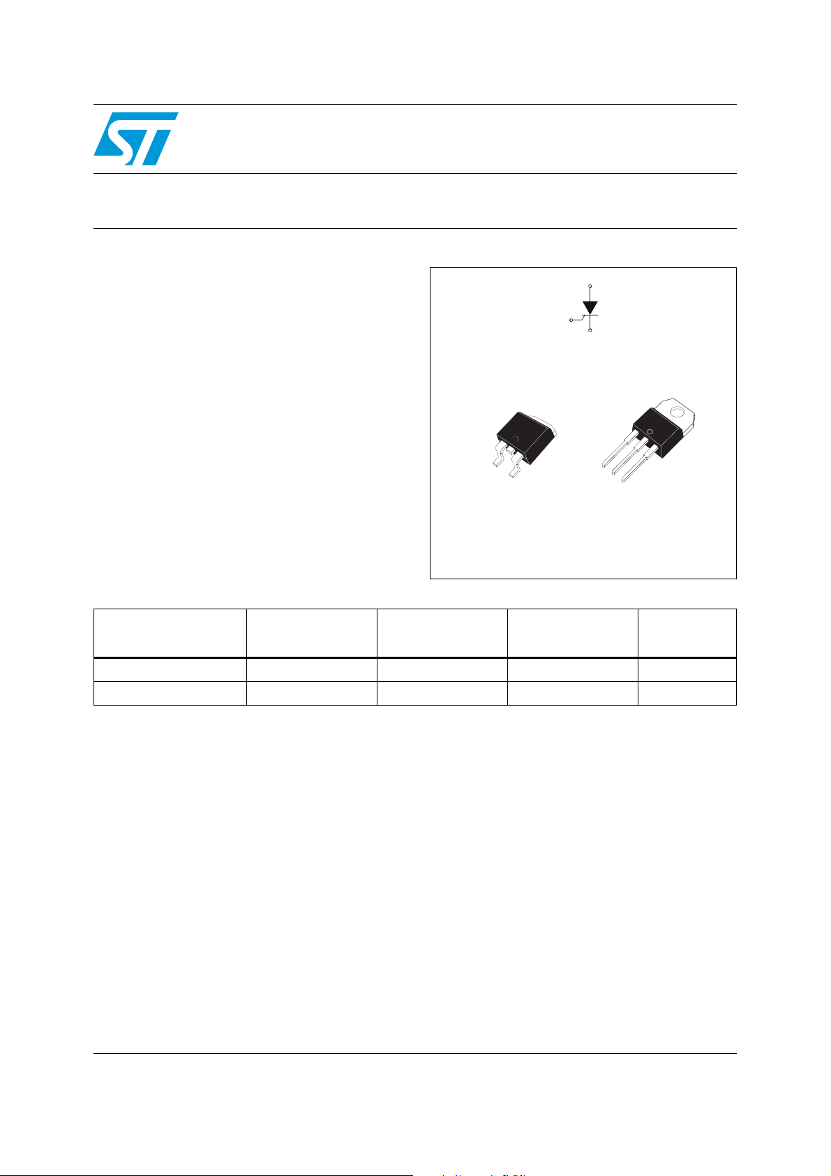
Description
The standard TN16 / TYNx16 16 A SCRs series
is suitable for general purpose applications.
Using clip assembly technology, they provide a
superior performance in surge current
K
A
capabilities.
(TN1625-x00G)
Table 1. Device summary
Parameter
V
DRM/VRRM
Sensitivity 25 25 25 mA
TN1625-600G
TYN616RG TYN816RG
600 800 1000 V
A
G
D2PAK
TN1625-1000G
K
A
G
TO-220AB
(TYNx16RG)
Unit
A
November 2007 Rev 6 1/9
www.st.com
9
Characteristics TN1625, TYN616, TYN816
1 Characteristics
Table 2. Absolute ratings (limiting values)
Symbol Parameter Value Unit
I
T(RMS)
I
T(AV)
I
TSM
I
dI/dt
I
GM
P
G(AV)
T
V
RGM
Table 3. Electrical characteristics (Tj = 25 °C, unless otherwise specified)
RMS on-state current (180 °Conduction angle) Tc = 110 °C 16 A
Average on-state current (180 °Conduction angle) Tc = 110 °C 10 A
t
= 8.3 ms
Non repetitive surge peak on-state current
2
tI2t Value for fusing tp = 10 ms Tj = 25 °C 180 A
Critical rate of rise of on-state current
= 2 x IGT , tr ≤ 100 ns
I
G
p
tp = 10 ms 190
F = 60 Hz T
= 25 °C
T
j
= 125 °C 50 A/µs
j
200
Peak gate current tp = 20 µs Tj = 125 °C 4 A
Average gate power dissipation Tj = 125 °C 1 W
Storage junction temperature range
stg
T
Operating junction temperature range
j
- 40 to + 150
- 40 to + 125
Maximum peak reverse gate voltage 5 V
Symbol Test Conditions Value Unit
I
GT
VD = 12 V RL = 33 Ω
V
GT
V
I
dV/dt V
V
V
R
I
DRM
I
RRM
Table 4. Thermal resistance
VD = V
GD
IT = 500 mA Gate open MAX. 40 mA
H
I
IG = 1.2 x I
L
= 67 % V
D
ITM = 32 A tp = 380 µs Tj = 25 °C MAX. 1.6 V
TM
Threshold voltage Tj = 125 °C MAX. 0.77 V
t0
Dynamic resistance Tj = 125 °C MAX. 23 mΩ
d
V
DRM
RL = 3.3 kΩ Tj = 125 °C MIN. 0.2 V
DRM
GT
Gate open Tj = 125 °C MIN. 500 V/µs
DRM
= V
RRM
Tj = 25 °C
T
= 125 °C 2 mA
j
MIN. 2
MAX. 25
MAX. 1.3 V
MAX. 60 mA
5µA
MAX.
mA
A
°C
2
S
Symbol Parameter Value Unit
R
th(j-c)
R
th(j-a)
S = copper surface under tab
Junction to case (DC) 1.1 °C/W
S = 01 cm
2
D2PA K 4 5
Junction to ambient (DC)
TO-220AB 60
2/9
°C/W
TN1625, TYN616, TYN816 Characteristics
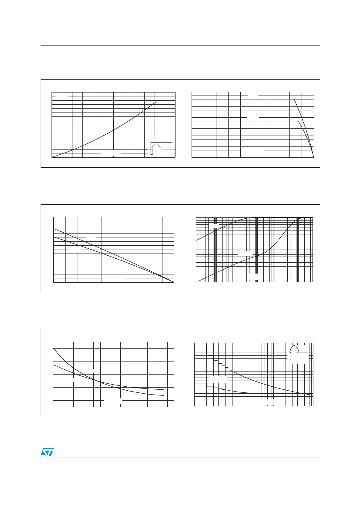
Figure 1. Maximum average power
dissipation versus average on-state
current
P(W)
16
α = 180°
14
12
10
8
6
4
2
0
024681012
I (A)
T(AV)
360°
α
Figure 3. Average and D.C. on-state current
versus ambient temperature
(copper surface under tab: S=1cm
2
(D
PAK )
I (A)
T(AV)
4.0
3.5
3.0
2.5
2.0
1.5
1.0
0.5
0.0
α = 180°
0 25 50 75 100 125
D.C.
T (°C)
amb
Figure 2. Average and D.C. on-state current
versus case temperature
I (A)
T(AV)
18
16
14
12
10
8
6
4
2
0
0 25 50 75 100 125
D.C.
α = 180°
T (°C)
case
Figure 4. Relative variation of thermal
impedance versus pulse duration
2
)
K=[Z /R
1.00
0.10
0.01
1E-3 1E-2 1E-1 1E+0 1E+1 1E+2 5E+2
th th
Z
th(j-c)
]
Z
th(j-a)
t (s)
p
Figure 5. Relative variation of gate trigger
current, holding current and
latching current versus junction
temperature
I,I,I[T] /
GT H L j
2.5
2.0
1.5
1.0
0.5
0.0
-40 -20 0 20 40 60 80 100 120 140
I ,I ,I [T =25°C]
GT H L j
I
GT
IH& I
L
T (°C)
j
Figure 6. Surge peak on-state current versus
number of cycles
I (A)
TSM
200
180
160
140
120
100
80
60
40
20
0
1 10 100 1000
Repetitive
T =110°C
C
Non repetitive
T initial=25°C
j
Number of cycles
3/9
t =10ms
p
One cycle
 Loading...