

ST TSV991, TSV992, TSV994, TSV991A, TSV992A User Manual
...
Features
TSV991, TSV992, TSV994
TSV991A, TSV992A, TSV994A
Rail-to-rail input/output 20 MHz GBP operational amplifiers
■ Low input offset voltage: 1.5 mV max (A grade)
■ Rail-to-rail input and output
■ Wide bandwidth 20 MHz, stable for gain ≥ 3
■ Low power consumption: 820 µA typ
■ High output current: 35 mA
■ Operating from 2.5 V to 5.5 V
■ Low input bias current, 1 pA typ
■ ESD internal protection ≥ 5kV
■ Latch-up immunity
Applications
■ Battery-powered applications
■ Portable devices
■ Signal conditioning
■ Active filtering
■ Medical instrumentation
■ Automotive applications
Description
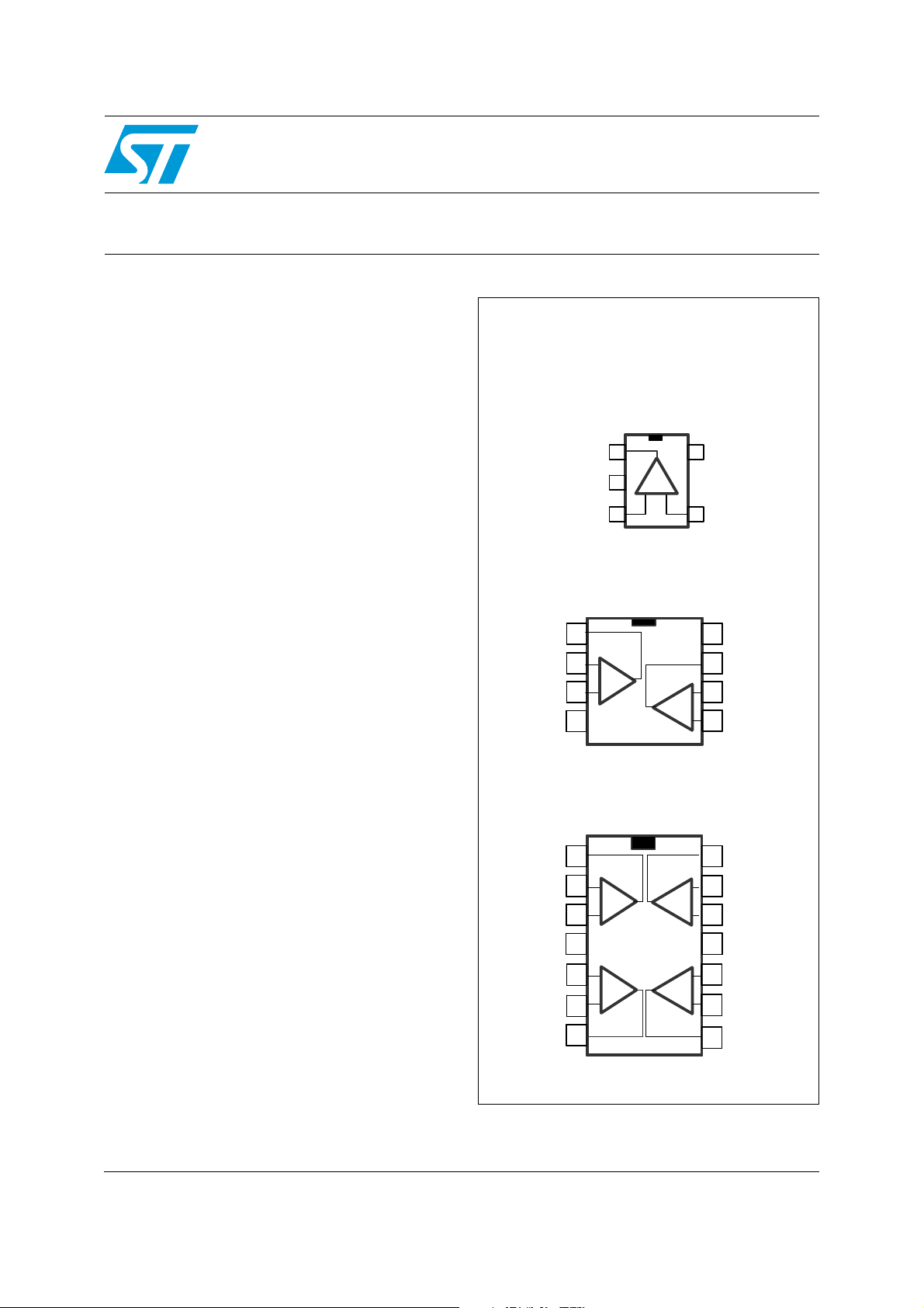
The TSV991/2/4 family of single, dual and quad
operational amplifiers offers low voltage operation
and rail-to-rail input and output.
These devices feature an excellent speed/power
consumption ratio, offering a 20 MHz gainbandwidth, stable for gains above 3 (100 pF
capacitive load), while consuming only 1.1 mA
maximum at 5 V. They also feature an ultra-low
input bias current.
These characteristics make the TSV991/2/4
family ideal for sensor interfaces, battery-supplied
and portable applications, as well as active
filtering.
Out1
Out1
In1-
In1-
In1+
In1+
V
V
CC-
CC-
Out1
Out1
In1-
In1-
In1+
In1+
V
V
CC+
CC+
In2+
In2+
In2-
In2-
Out2
Out2
Pin connections
(top view)
SOT23-5
Out
1
V
2
CC-
3
In+
MiniSO-8, SO-8
1
1
_
_
2
2
+
+
3
3
4
4
SO-14, TSSOP14
1
1
_
_
2
2
+
+
3
3
4
4
5
5
+
+
_
_
6
6
7
7
V
5
CC+
In-
4
8
8
V
V
CC+
CC+
7
7
Out2
Out2
_
_
+
+
_
_
+
+
+
+
_
_
14
14
13
13
12
12
11
11
10
10
In2-
In2-
6
6
In2+
In2+
5
5
Out4
Out4
In4-
In4-
In4+
In4+
V
V
CC-
CC-
In3+
In3+
In3-
In3-
9
9
Out3
Out3
8
8
January 2010 Doc ID 12833 Rev 8 1/20
www.st.com
20
Absolute maximum ratings and operating conditions TSV99x-TSV99xA
1 Absolute maximum ratings and operating conditions
Table 1. Absolute maximum ratings
Symbol Parameter Value Unit
(3)
(4)
(1)
(8)
(2)
(7)
(9)
(5) (6)
V
CC-
6V
±V
CC
-0.2 to V
+0.2 V
CC+
V
10 mA
250
125
190
°C/W
103
100
81
40
39
°C/W
31
32
5kV
400 V
1500
750
V
500
V
CC
V
id
V
in
I
in
T
stg
R
thja
R
thjc
T
ESD
Supply voltage
Differential input voltage
Input voltage
Input current
Storage temperature -65 to +150 °C
Thermal resistance junction to ambient
SOT23-5
SO-8
MiniSO-8
SO-14
TSSOP14
Thermal resistance junction to case
SOT23-5
SO-8
MiniSO-8
SO-14
TSSOP14
Maximum junction temperature 150 °C
j
HBM: human body model
MM: machine model
CDM: charged device model
SOT23-5, SO-8, MiniSO-8
TSSOP14
SO-14
Latch-up immunity 200 mA
1. Value with respect to VDD pin.
2. Differential voltages are the non-inverting input terminal with respect to the inverting input terminal.
3. VCC-Vin must not exceed 6 V.
4. Input current must be limited by a resistor in series with the inputs.
5. Short-circuits can cause excessive heating and destructive dissipation.
are typical values.
6. R
th
7. Human body model: 100 pF discharged through a 1.5 kΩ resistor between two pins of the device, done for
all couples of pin combinations with other pins floating.
8. Machine model: 200 pF charged to the specified voltage, then discharged directly between two pins of the
device with no external series resistor (internal resistor < 5 Ω), done for all couples of pin combinations with
other pins floating.
9. Charged device model: all pins plus package are charged together to the specified voltage and then
discharged directly to the ground.
2/20 Doc ID 12833 Rev 8
TSV99x-TSV99xA Absolute maximum ratings and operating conditions
Table 2. Operating conditions
Symbol Parameter Value Unit
V
CC
V
icm
T
Supply voltage 2.5 to 5.5 V
Common mode input voltage range V
Operating free air temperature range -40 to +125 °C
op
-0.1 to V
CC-
+0.1 V
CC+
Doc ID 12833 Rev 8 3/20
Electrical characteristics TSV99x-TSV99xA
2 Electrical characteristics
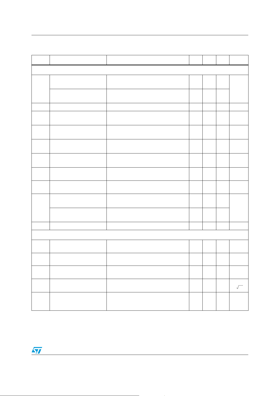
Table 3. Electrical characteristics at V
to V
/2, full temperature range (unless otherwise specified)
CC
= +2.5 V, V
CC+
CC-
= 0 V, V
= VCC/2, with RL connected
icm
(1)
Symbol Parameter Conditions Min. Typ. Max. Unit
DC performance
V
io
DV
I
io
I
ib
CMR
A
vd
VCC-
V
OH
V
OL
I
out
I
CC
Offset voltage
TSV99x
TSV99xA
Input offset voltage drift - 2 - µV/°C
io
/2)
/2)
(2)
(2)
Input offset current
(V
out=VCC
Input bias current
(V
out=VCC
Common mode rejection
ratio 20 log (ΔV
/ΔVio)
ic
Large signal voltage gain
High level output voltage
Low level output voltage
I
sink
I
source
Supply current (per operator) No load, V
Top= 25° C
< Top < T
T
min
max
Top= 25° C
< Top < T
T
min
= 25° C
T
op
T
< Top < T
min
= 25° C
T
op
< Top < T
T
min
0V to 2.5V, V
< Top < T
T
min
RL= 10 kΩ, V
< Top < T
T
min
=10kΩ, T
R
L
RL=600Ω, T
R
=10kΩ, T
L
RL=600Ω, T
max
max
max
= 1.25 V, Top= 25° C
out
max
= 0.5 V to 2 V, Top= 25° C
out
max
< Top < T
min
< Top < T
min
< Top < T
min
< Top < T
min
Vo = 2.5 V, Top= 25° C
< Top < T
T
min
max
Vo = 0 V, T = 25° C
< Top < T
T
min
max
out=VCC/2, Tmin
max
max
max
max
< Top < T
max
-
0.1-4.5
-
-
-
-
-
-
-
585375
807589
7.5
-
1.5
-
3
1
-10100
1
-10100
-dB
-
-
-
154540
150
154540
-
181632
181635
150
-
-
-
-
-
-
- 0.78 1.1 mA
mV
mV
mV
mA
AC performance
pA
pA
dB
R
=2kΩ, CL= 100 pF, f = 100 kHz,
GBP Gain bandwidth product
Gain Minimum gain for stability
SR Slew rate R
Equivalent input noise
e
n
voltage
THD+N Total harmonic distortion
1. All parameter limits at temperatures other than 25° C are guaranteed by correlation.
2. Guaranteed by design.
L
=25°C
T
op
Phase margin = 60°, R
= 100 pF, Top= 25° C
C
L
=2kΩ, CL= 100 pF, Top= 25° C - 10 - V/µs
L
f = 10 kHz, T
= 25° C - 21 -
op
G=1, f=1kHz, R
V
=(VCC+1)/2, V
icm
=25°C
T
op
= 10kΩ, RL=2kΩ,
f
=2kΩ, Bw = 22 kHz,
L
=1.1Vpp,
out
4/20 Doc ID 12833 Rev 8
-20- MHz
5V/V
nV
-----------Hz
0.0017
-
-%
TSV99x-TSV99xA Electrical characteristics
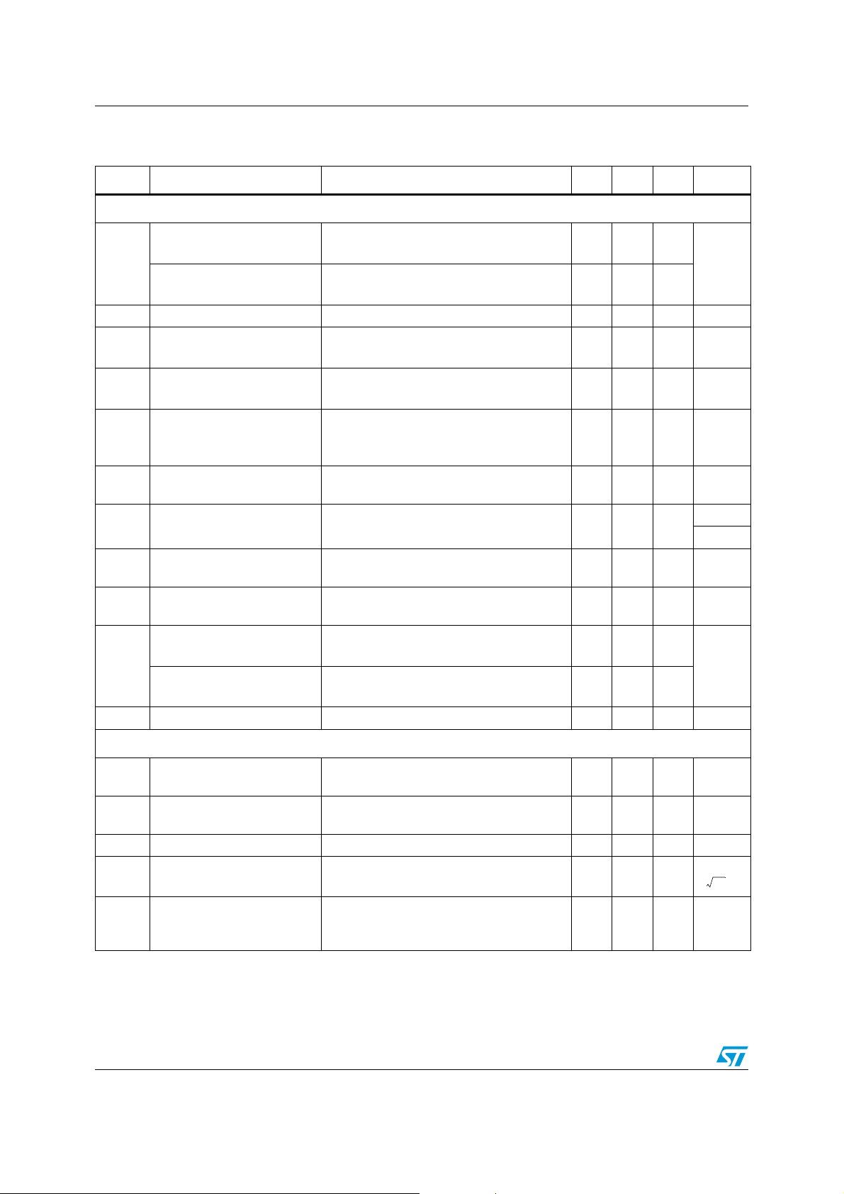
Table 4. Electrical characteristics at V
to V
/2, full temperature range (unless otherwise specified)
CC
= +3.3 V, V
CC+
CC-
= 0 V, V
= VCC/2, with RL connected
icm
(1)
Symbol Parameter Conditions Min. Typ. Max. Unit
DC performance
V
io
DV
I
io
I
ib
CMR
A
vd
V
CC
V
OH
V
OL
I
out
I
CC
Offset voltage
TSV99x
TSV99xA
Input offset voltage drift - 2 - µV/°C
io
/2)
/2)
(2)
(2)
Input offset current
(V
out=VCC
Input bias current
(V
out=VCC
Common mode rejection
ratio 20 log (ΔV
/ΔVio)
ic
Large signal voltage gain
High level output voltage
Low level output voltage
I
sink
I
source
Supply current (per operator) No load, V
Top= 25° C
T
< Top < T
min
= 25° C
T
op
T
< Top < T
min
= 25° C
T
op
< Top < T
T
min
= 25° C
T
op
< Top < T
T
min
0V to 3.3V, V
< Top < T
T
min
R
=10kΩ, V
L
< Top < T
T
min
=10kΩ, T
R
L
RL=600Ω, T
=10kΩ, T
R
L
RL=600Ω, T
max
max
max
max
= 1.65 V, Top= 25° C
out
max
= 0.5 V to 2.8 V, T=25° C
out
max
< Top < T
min
< Top < T
min
< Top < T
min
< Top < T
min
Vo = 3.3 V, Top= 25° C
T
< Top < T
min
max
Vo = 0 V, Top= 25° C
T
< Top < T
min
max
out=VCC
/2, T
max
max
max
max
< Top < T
min
max
-
0.1-4.5
-
-
-
-
-
-
-
605578
807590
7.5
-
1.5
-
3
1
-10100
1
-10100
-dB
-
-
-
154540
150
154540
-
181632
181635
150
-
-
-
-
-
-
-0.81.1mA
mV
mV
mV
mA
AC performance
pA
pA
dB
=2kΩ, CL= 100 pF, f = 100 kHz,
R
GBP Gain bandwidth product
Gain Minimum gain for stability
SR Slew rate
Equivalent input noise
e
n
voltage
THD+N Total harmonic distortion
L
= 25° C
T
op
Phase margin = 60°, R
= 10kΩ, RL=2kΩ,
f
CL= 100 pF, Top= 25° C
=2kΩ, CL= 100 pF, f = 100 kHz,
R
L
= 25° C
T
op
f = 10 kHz, T
G=1, f=1kHz, R
=(VCC+1)/2, V
V
icm
= 25° C - 21 -
op
=2kΩ, Bw = 22 kHz,
L
=1.9Vpp,
out
Top= 25° C
1. All parameter limits at temperatures other than 25°C are guaranteed by correlation.
2. Guaranteed by design.
Doc ID 12833 Rev 8 5/20
-20-MHz
5V/V
-10-V/µs
nV
-----------Hz
-0.001- %
Electrical characteristics TSV99x-TSV99xA
Table 5. Electrical characteristics at V
R
connected to VCC/2, full temperature range (unless otherwise specified)
L
= +5 V, V
CC+
= 0 V, V
CC-
= VCC/2,
icm
(1)
Symbol Parameter Conditions Min. Typ. Max. Unit
DC performance
V
io
DV
I
io
I
ib
CMR
SVR
A
vd
V
CC
V
OH
V
OL
I
out
I
CC
Offset voltage
TSV99x
TSV99xA
Input offset voltage drift - 2 - µV/°C
io
/2)
/2)
(2)
(2)
Input offset current
(V
out=VCC
Input bias current
(V
out=VCC
Common mode rejection
ratio
20 log (ΔV
/ΔVio)
ic
Supply voltage rejection ratio
20 log (ΔV
/ΔVio)
cc
Large signal voltage gain
High level output voltage
Low level output voltage
I
sink
I
source
Supply current (per operator) No load, V
Top= 25° C
T
< Top < T
min
= 25° C
T
op
< Top < T
T
min
= 25° C
T
op
< Top < T
T
min
= 25° C
T
op
T
< Top < T
min
0V to 5V, V
< Top < T
T
min
= 2.5 to 5 V 70 86 - dB
V
CC
RL=10kΩ, V
< Top < T
T
min
=10kΩ, T
R
L
RL=600Ω, T
=10kΩ, T
R
L
RL=600Ω, T
max
max
max
max
= 2.5 V,Top= 25° C
out
max
= 0.5 V to 4.5 V, T = 25° C
out
max
< Top < T
min
< Top < T
min
< Top < T
min
< Top < T
min
max
max
max
max
Vo = 5 V, Top= 25° C
T
< T
amb
< T
max
min
Vo = 0 V, Top= 25° C
< T
T
min
amb
out
< T
max
=2.5V, T
< Top < T
min
max
-
0.1-4.5
-
-
-
-
-
-
-
7.5
-
1.5
-
3
1
10
-
100
1
10
-
100
625782
807591
-
154540
150
154540
150
181632
-
181635
-
- 0.82 1.1 mA
mV
-dB
-
-
mV
mV
-
mA
-
-
AC performance
pA
pA
dB
dB
R
=2kΩ, CL= 100 pF, f = 100 kHz,
GBP Gain bandwidth product
Gain Minimum gain for stability
SR Slew rate R
Equivalent input noise
e
n
voltage
L
Top= 25° C
Phase margin = 60°, R
= 10kΩ, RL=2kΩ,
f
CL= 100 pF, Top= 25° C
=2kΩ, CL= 100 pF, Top= 25° C - 10 - V/µs
L
f = 10 kHz, T
= 25° C - 21 -
op
G=1, f=1kHz, RL=2kΩ, Bw = 22 kHz,
THD+N Total harmonic distortion
1. All parameter limits at temperatures other than 25°C are guaranteed by correlation.
2. Guaranteed by design.
V
=(VCC+1)/2, V
icm
= 25° C
T
op
=3.6Vpp,
out
6/20 Doc ID 12833 Rev 8
-20-MHz
5V/V
nV
-----------Hz
0.000
-
-%
7
 Loading...