

ST TSV912H, TSV912AH User Manual
rail-to-rail input/output 8 MHz operational amplifiers
Features
■ Rail-to-rail input and output
■ Wide bandwidth
■ Low power consumption: 820 µA typ
■ Unity gain stability
■ High output current: 35 mA
■ Operating range from 2.5 to 5.5 V
■ Low input bias current, 1 pA typ
■ ESD internal protection ≥ 5kV
■ Latch-up immunity
Applications
TSV912H, TSV912AH
High temperature
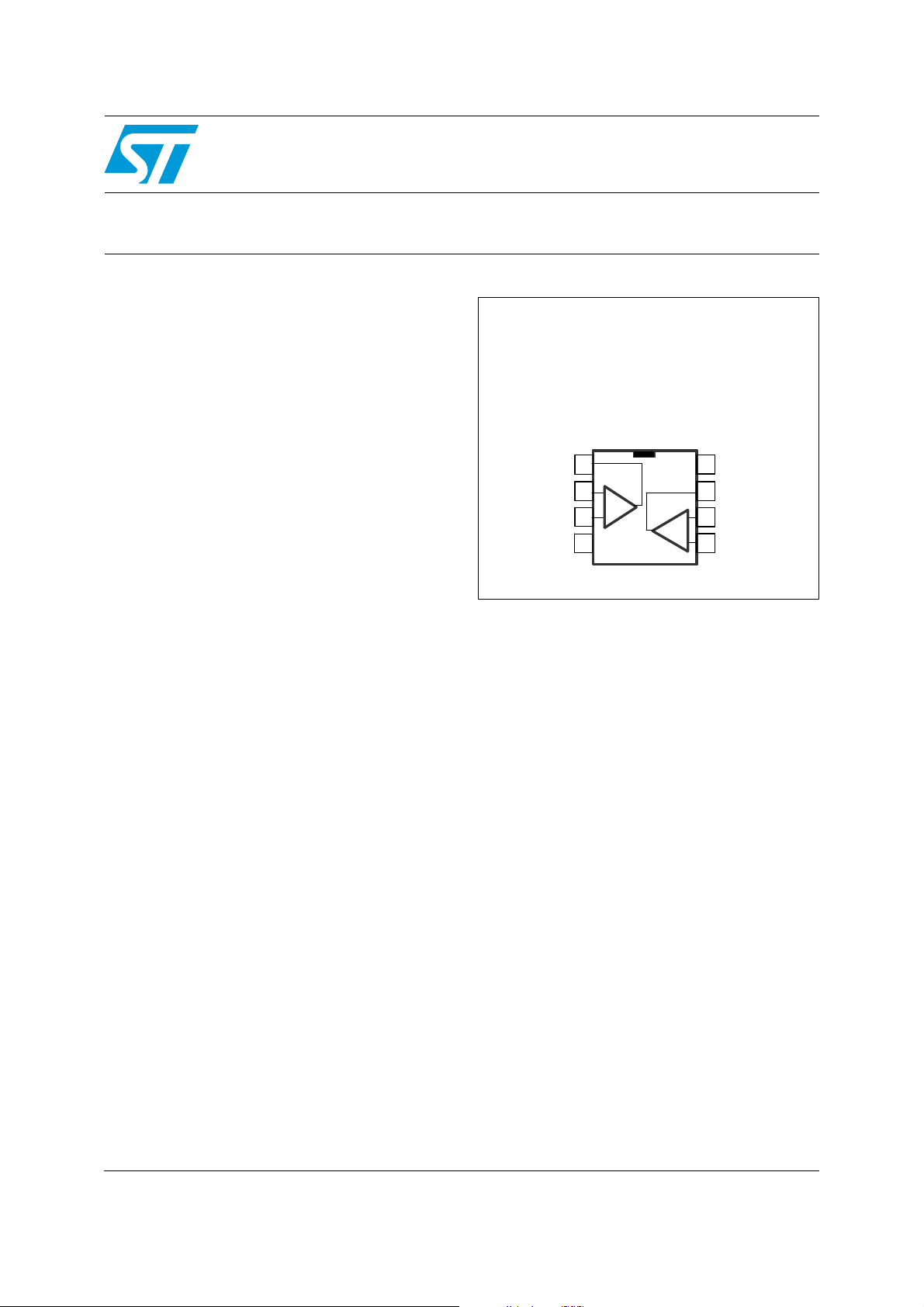
Pin connections
(top view)
SO-8
Out1
Out1
In1-
In1-
In1+
In1+
V
V
CC-
CC-
1
1
_
_
2
2
+
+
3
3
4
4
8
8
V
V
CC+
CC+
7
7
Out2
Out2
_
_
+
+
In2-
In2-
6
6
In2+
In2+
5
5
■ Automotive products
Description
The TSV912H and TSV912AH operational
amplifiers offer low voltage operation and rail-torail input and output.
The devices feature an excellent speed/power
consumption ratio, offering an 8 MHz gainbandwidth product while consuming only 1.1 mA
maximum at 5 V. They are unity gain stable and
feature an ultra-low input bias current.
The TSV912H is a high temperature version of
the TSV912, and can operate from -40°C to
+150°C with unique characteristics. Its main
target applications are automotive, but the device
is also ideal for sensor interfaces, batterysupplied and portable applications, as well as
active filtering.
July 2010 Doc ID 17688 Rev 1 1/16
www.st.com
16
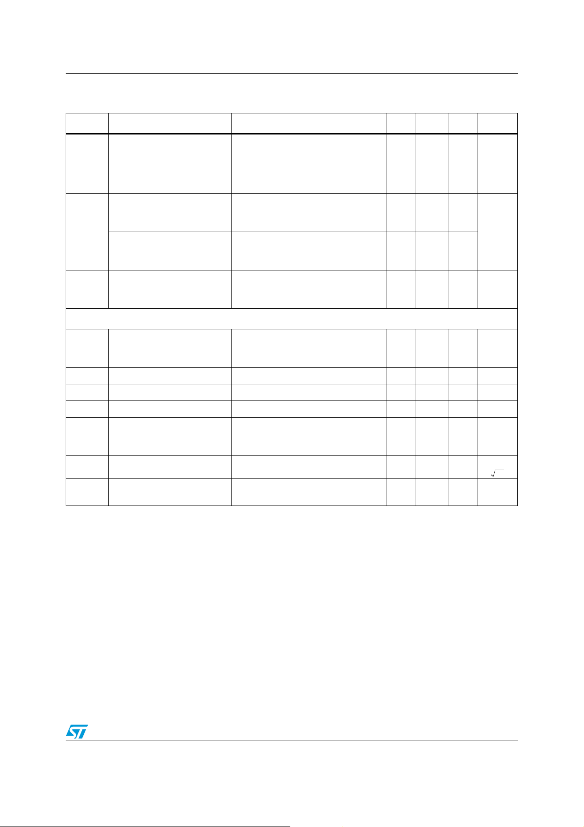
Absolute maximum ratings and operating conditions TSV912H, TSV912AH
1 Absolute maximum ratings and operating conditions
Table 1. Absolute maximum ratings
Symbol Parameter Value Unit
(3)
(4)
(1)
(V
CC+
(8)
- V
(2)
(7)
CC-
(9)
)
V
CC-
6V
±V
CC
-0.2 to V
+0.2 V
CC+
V
10 mA
(5) (6)
125
(5) (6)
°C/W
°C/W
5kV
400 V
1500 V
V
CC
V
V
I
in
T
stg
R
thja
R
thjc
T
Supply voltage
Differential input voltage
id
Input voltage
in
Input current
Storage temperature -65 to +150 °C
Thermal resistance junction to ambient
SO-8
Thermal resistance junction to case
SO-8 40
Maximum junction temperature 160 °C
j
HBM: human body model
ESD
MM: machine model
CDM: charged device model
Latch-up immunity 200 mA
1. All voltage values, except differential voltage, are with respect to network ground terminal.
2. Differential voltages are the non-inverting input terminal with respect to the inverting input terminal.
3. VCC-Vin must not exceed 6 V.
4. Input current must be limited by a resistor in series with the inputs.
5. Short-circuits can cause excessive heating and destructive dissipation.
are typical values.
6. R
th
7. Human body model: a 100 pF capacitor is charged to the specified voltage, then discharged through a
1.5kΩ resistor between two pins of the device. This is done for all couples of connected pin combinations
while the other pins are floating.
8. Machine model: a 200 pF capacitor is charged to the specified voltage, then discharged directly between
two pins of the device with no external series resistor (internal resistor < 5 Ω). This is done for all couples of
connected pin combinations while the other pins are floating.
9. Charged device model: all pins and the package are charged together to the specified voltage and then
discharged directly to the ground through only one pin. This is done for all pins.
Table 2. Operating conditions
Symbol Parameter Value Unit
T
V
V
CC
icm
oper
Supply voltage (V
CC+
- V
) 2.5 to 5.5 V
CC-
Common mode input voltage range V
Operating free-air temperature range -40 to +150 °C
2/16 Doc ID 17688 Rev 1
-0.1 to V
CC-
+0.1 V
CC+
TSV912H, TSV912AH Electrical characteristics
2 Electrical characteristics
Table 3. Electrical characteristics at V
Symbol Parameter Conditions Min. Typ. Max. Unit
DC performance
to V
/2, T = 25°C (unless otherwise specified)
CC
= +2.5 V with V
CC+
CC-
= 0 V, V
= VCC/2, RL connected
icm
V
DV
CMR
A
Input offset voltage
io
/DT Input offset voltage drift
io
Input offset current
I
io
I
Input bias current
ib
Common mode rejection ratio
20 log (ΔV
Large signal voltage gain
vd
/ΔVio)
ic
VCC-VOHHigh level output voltage
V
I
I
Low level output voltage
OL
I
sink
out
I
source
Supply current (per operator)
CC
AC performance
TSV912H, T=25°C
TSV912H, T
< T < T
min
TSV912AH, T=25°C
TSV912AH, T
< T < T
min
-40°C < T < +125°C
+125°C < T < +150°C
V
out=VCC
/2
T=25°C
< T < T
T
min
V
out=VCC
max
/2
T=25°C
T
< T < T
min
0V to 2.5V, V
max
out
= 1.25V
T=25°C
< T < T
T
min
R
= 10kΩ, V
L
max
= 0.5V to 2V
out
T=25°C
< T < T
T
min
max
RL=10kΩ, T=25°C
RL=10kΩ, T
min
< T < T
RL=600Ω, T=25°C
RL=600Ω, T
R
=10kΩ, T=25°C
L
RL=10kΩ, T
min
min
< T < T
< T < T
RL=600Ω, T=25°C
R
=600Ω, T
L
V
= 2.5V
out
< T < T
min
T=25°C
T
< T < T
min
V
= 0V
out
max
T=25°C
< T < T
T
min
No load, V
max
out=VCC
/2
T=25°C
< T < T
T
min
max
max
max
max
max
max
max
58
53
80
70
18
14
18
14
0.1 4.5
7.5
1.5
3
2
20
110
μV/°C
(1)
5
110
(1)
5
75 dB
89 dB
15
40
60
45
150
250
15
40
60
45
150
250
32
35
0.78 1.1
1.1
mV
pA
nA
pA
nA
mV
mV
mA
mA
GBP Gain bandwidth product
RL=2kΩ, CL=100pF, f =100kHz
T=25°C
< T < T
T
min
max
8
4
Doc ID 17688 Rev 1 3/16
MHz
Electrical characteristics TSV912H, TSV912AH
Table 3. Electrical characteristics at V
to V
/2, T = 25°C (unless otherwise specified) (continued)
CC
= +2.5 V with V
CC+
CC-
= 0 V, V
= VCC/2, RL connected
icm
Symbol Parameter Conditions Min. Typ. Max. Unit
F
Unity gain frequency RL=2kΩ, CL= 100pF 7.2 MHz
u
φm Phase margin RL=2kΩ, CL= 100pF 45 Degrees
G
Gain margin RL=2kΩ, CL= 100pF 8 dB
m
RL=2kΩ, CL=100pF, Av=1
SR Slew rate
e
Equivalent input noise voltage f= 10kHz 21
n
THD+enTotal harmonic distortion
1. Guaranteed by design.
Table 4. Electrical characteristics at V
to V
/2, T = 25°C (unless otherwise specified)
CC
T=25°C
< T < T
T
min
max
G=1, f=1kHz, R
=(VCC+1)/2, V
V
icm
= +3.3 V with V
CC+
=2kΩ, Bw= 22kHz,
L
=1.1V
out
pp
CC-
= 0 V, V
4.5
3.5
0.001 %
= VCC/2, RL connected
icm
Symbol Parameter Conditions Min. Typ. Max. Unit
DC performance
V
DV
I
I
CMR
A
V
CC-VOH
Input offset voltage
io
Input offset voltage drift
io
Input offset current
io
Input bias current
ib
Common mode rejection ratio
20 log (ΔVic/ΔVio)
Large signal voltage gain
vd
High level output voltage
TSV912H, T=25°C
TSV912H, T
< T < T
min
TSV912AH, T=25°C
TSV912AH, T
min
< T < T
-40°C < T < +125°C
+125°C < T < +150°C
V
out=VCC
/2
T=25°C
< T < T
T
min
V
out=VCC
max
/2
T=25°C
< T < T
T
min
0V to 3.3V, V
max
out
= 1.65V
T=25°C
< T < T
T
min
R
=10kΩ, V
L
max
= 0.5V to 2.8V
out
T=25°C
< T < T
T
min
R
=10kΩ, T=25°C
L
=10kΩ, T
R
L
max
min
< T < T
RL=600Ω, T=25°C
RL=600Ω, T
< T < T
min
max
max
60
55
80
70
max
max
0.1 4.5
7.5
1.5
3
2
20
110
μV/°C
(1)
5
110
(1)
5
78 dB
90 dB
15
40
60
45
150
250
V/μs
nV
-----------Hz
mV
pA
nA
pA
nA
mV
4/16 Doc ID 17688 Rev 1
TSV912H, TSV912AH Electrical characteristics
Table 4. Electrical characteristics at V
to V
/2, T = 25°C (unless otherwise specified) (continued)
CC
= +3.3 V with V
CC+
CC-
= 0 V, V
= VCC/2, RL connected
icm
Symbol Parameter Conditions Min. Typ. Max. Unit
R
=10kΩ, T=25°C
L
=10kΩ, T
R
V
Low level output voltage
OL
L
min
< T < T
max
RL=600Ω, T=25°C
=600Ω, T
R
L
V
= 3.3V
I
sink
I
out
I
source
out
T=25°C
< T < T
T
min
V
= 0V
out
T=25°C
< T < T
T
min
No load, V
I
Supply current (per operator)
CC
T=25°C
< T < T
T
min
< T < T
min
max
max
out=VCC
max
max
18
14
18
14
/2
15
40
60
45
150
250
32
35
0.8 1.1
1.1
AC performance
R
=2kΩ, CL= 100pF, f = 100kHz,
GBP Gain bandwidth product
Unity gain frequency RL= 2kΩ, CL=100pF 7.2 MHz
F
u
φm Phase margin R
G
Gain margin RL=2kΩ, CL=100pF 8 dB
m
SR Slew rate
Equivalent input noise voltage f= 10kHz 21
e
n
THD+e
1. Guaranteed by design.
Total harmonic distortion
n
L
T=25°C
< T < T
T
min
=2kΩ, CL=100pF 45 Degrees
L
R
=2kΩ, CL= 100pF, Av=1,
L
max
T=25°C
< T < T
T
min
G=1, f=1kHz, R
=(VCC+1)/2, V
V
icm
max
=2kΩ, BW= 22kHz,
L
=1.9Vpp,
out
8
4.2
4.5
3.5
0.0007 %
mV
mA
mA
MHz
V/μs
nV
-----------Hz
Doc ID 17688 Rev 1 5/16
 Loading...