

Features
■ Low supply current: 4.5 mA
■ High speed: 150 MHz - 110 V/μs
■ Unity gain stability
■ Low offset voltage: 4 mV
■ Low noise 4.2 nV/√ Hz
■ Specified for 600 Ω and 150 Ω loads
■ High video performances:
– differential gain: 0.03%
– differential phase: 0.07°
– gain flatness: 6 MHz, 0.1 dB max. at 10 db
gain
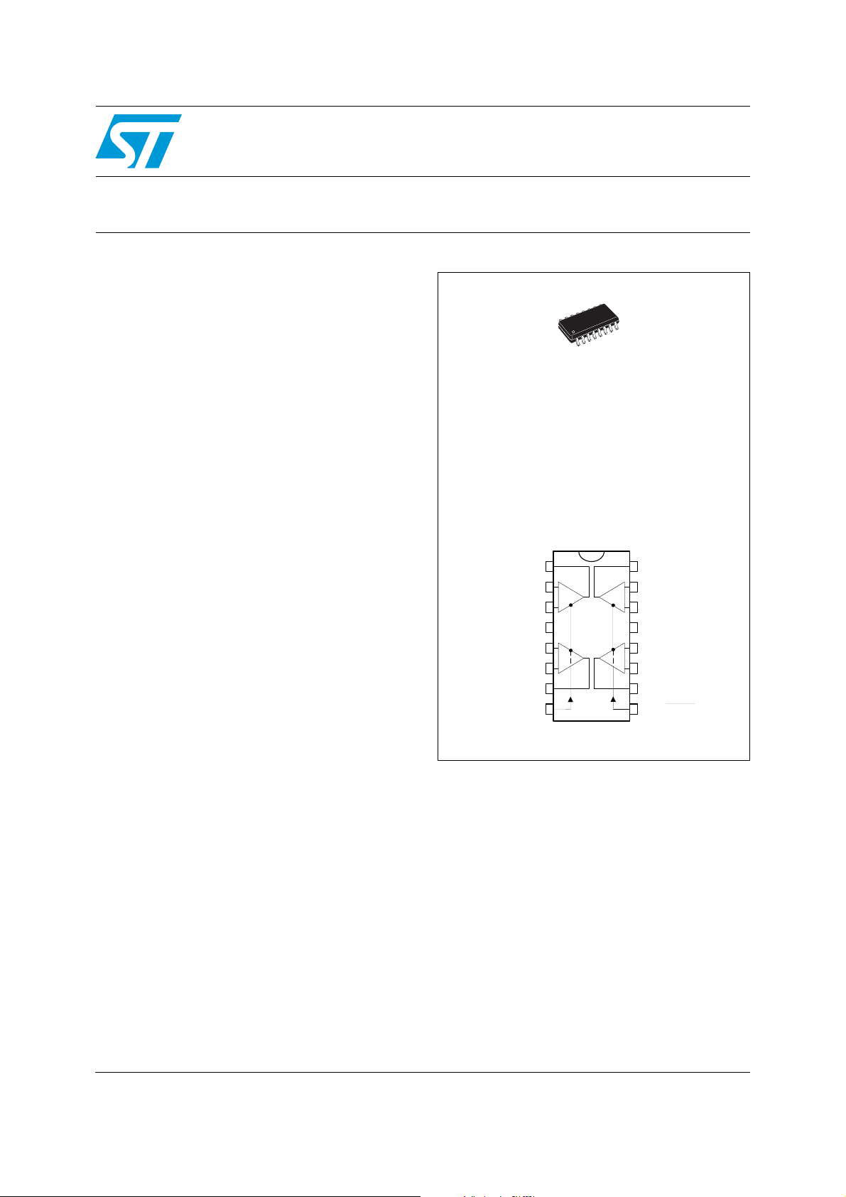
TSH95
High-speed low-power quad operational
amplifier with dual standby position
D
SO16
(Plastic micropackage)
Pin connections (top view)
Applications
■ Video buffers
■ A/D converter drivers
Description
The TSH95 is a low-power, high-frequency quad
operational amplifier designated for high-quality
video processing. The device offers an excellent
speed consumption ratio with 4.5 mA per
amplifier for a 150 MHz bandwidth.
A high slew rate and low noise also make it
suitable for high-quality audio applications.
The TSH95 offers two separate complementary
STANDBY pins: STANDBY 1 acting on operators
1 and 2, and STANDBY 2 acting on operators 3
and 4.
These pins reduce the consumption of the
corresponding operators and put the output in a
high impedance state.
Output 1
Inverting Input 1
Non-inverting Input 1
V
Non-inverting Input 2
Inverting Input 2
Output 2
Standby 1
1
2
-
+
3
+
4
CC
5
+
-
6
7
8
+
+
16
15
-
14
13
12
11
10
Output 4
Inverting Input 4
Non-inverting Input 4
-
V
CC
Non-inverting Input 3
Inverting Input 3
Output 3
Standby 2
9
August 2009 Doc ID 5243 Rev 2 1/19
www.st.com
19
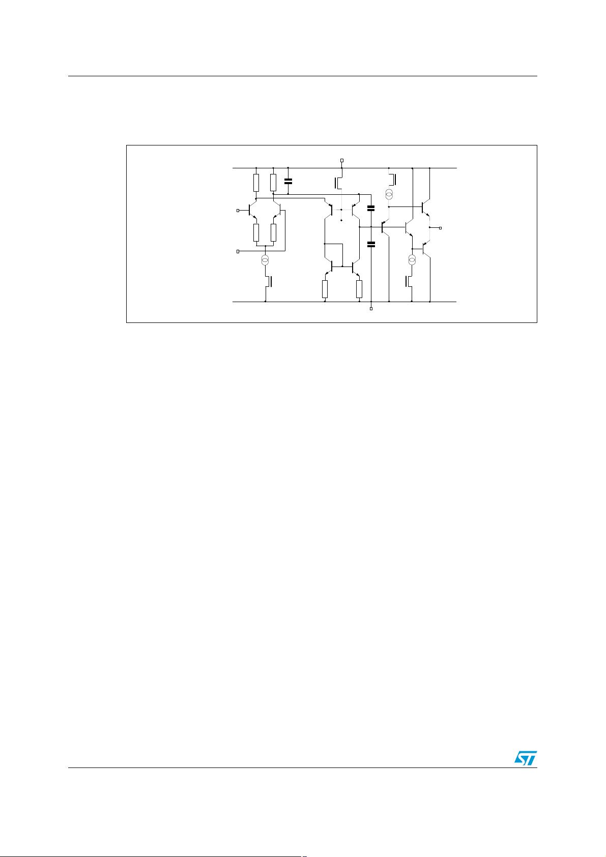
Schematic diagram TSH95
1 Schematic diagram
Figure 1. Schematic diagram
+
V
CC
non inverting
input
inverting
input
stdby
stdby
Internal
V
ref
stdby
output
C
c
stdby
-
V
CC
2/19 Doc ID 5243 Rev 2
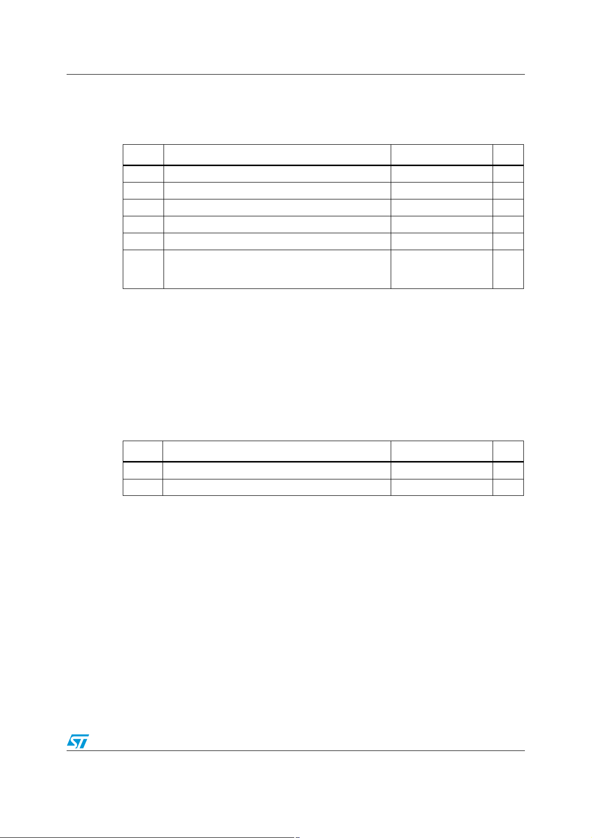
TSH95 Absolute maximum ratings and operating conditions
2 Absolute maximum ratings and operating conditions
Table 1. Absolute maximum ratings
Symbol Parameter Value Unit
(3)
(1)
(6)
(2)
(5)
(4)
CC
+
+0.3 V.
14 V
±5 V
-0.3 to 12 V
1.5
2
kV
kV
200
V
V
T
T
Supply voltage
CC
V
Differential input voltage
id
Input voltage
V
i
Operating free-air temperature range -40 to +125 °C
oper
Storage temperature range -65 to +150 °C
stg
CDM: charged device model
ESD
HBM: human body model
MM: machine model
1. All voltages values, except differential voltage, are with respect to network ground terminal.
2. Differential voltages are the non-inverting input terminal with respect to the inverting input terminal.
3. The magnitude of input and output voltages must never exceed V
4. Charged device model: all pins and the package are charged together to the specified voltage and then
discharged directly to the ground through only one pin. This is done for all pins.
5. Human body model: a 100 pF capacitor is charged to the specified voltage, then discharged through a
1.5 kΩ resistor between two pins of the device. This is done for all couples of connected pin combinations
while the other pins are floating.
6. Machine model: a 200 pF capacitor is charged to the specified voltage, then discharged directly between
two pins of the device with no external series resistor (internal resistor < 5 Ω). This is done for all couples of
connected pin combinations while the other pins are floating
Table 2. Operating conditions
Symbol Parameter Value Unit
V
Supply voltage 7 to 12 V
CC
Common mode input voltage range V
V
ic
CC
-
+2 to V
+
-1 V
CC
Doc ID 5243 Rev 2 3/19
Electrical characteristics TSH95
3 Electrical characteristics
Table 3. VCC+ = 5 V, VCC- = -5 V, pin 8 connected to 0 V, pin 9 connected to VCC+, T
amb
= 25° C
(unless otherwise specified)
Symbol Parameter Min. Typ. Max. Unit
V
I
CMR
SVR
Avd
Input offset voltage Vic = Vo = 0 V
io
I
io
I
ib
≤ T
T
min.
amb
≤ T
max.
Input offset current
≤ T
T
min.
amb
≤ T
max.
Input bias current
≤ T
T
min.
amb
≤ T
max.
Supply current (per amplifier, no load)
CC
T
min.
≤ T
amb
≤ T
max.
Common-mode rejection ratio V
≤ T
T
min.
amb
≤ T
max.
Supply voltage rejection ratio V
T
≤ T
amb
≤ T
max.
min.
Large signal voltage gain R
T
≤ T
amb
≤ T
max.
min.
CC
= 10 kΩ, Vo = ±2.5 V
L
High level output voltage Vid = 1 V
V
OH
T
≤ T
≤ T
min.
amb
R
max.
Low level output voltage Vid = 11 V
V
OL
≤ T
≤ T
T
min.
amb
R
max.
Output short circuit current Vid = ±1 V
I
o
T
≤ T
≤ T
min.
GBP
SR
Gain bandwidth product
= 100, RL = 600 Ω, CL = 15 pF, f = 7.5 MHz 90 150
A
VCL
Transition frequency 90 MHz
f
T
Slew rate
V
= -2 to +2 V, RL = 600 Ω, CL = 15 pF 62 110
in
e
Equivalent input voltage noise Rs = 50 Ω, f = 1 kHz 4.2 nV/√ Hz
n
φm Phase margin A
V
O1/VO2
Channel separation f = 1 MHz to 10 MHz 65 dB
amb
Source
max.
= +1 35 Degrees
VM
Gf Gain flatness f = DC to 6 MHz, A
THD Total harmonic distortion f = 1 kHz, V
12
515
4.5 6
= -3 V to +4 V, Vo = 0 V
ic
80
100
70
= ±5 V to ±3 V
60
75
50
57
70
54
RL = 600 Ω
= 150 Ω
R
L
= 150 Ω
L
= 600 Ω
R
L
RL = 150 Ω
= 150 Ω
L
Source
Sink
3
2.5
2.4
20
20
3.5
3
-3.5
-2.8
36
40 mA
15
Sink
= 10 dB 0.1 dB
VCL
= ±2.5 V, RL = 600 Ω 0.01 %
o
15
4
6
5
20
8
-3
-2.5
-2.4
mV
μA
μA
mA
dB
dB
dB
V
V
MHz
V/μs
4/19 Doc ID 5243 Rev 2
TSH95 Electrical characteristics
Table 3. VCC+ = 5 V, VCC- = -5 V, pin 8 connected to 0 V, pin 9 connected to VCC+, T
amb
= 25° C
(unless otherwise specified) (continued)
Symbol Parameter Min. Typ. Max. Unit
ΔG Differential gain f = 3.58 MHz, A
Δϕ Differential phase f = 3.58 MHz, A
Table 4. Standby mode: VCC+ = 5 V, VCC- = -5 V, T
Symbol Parameter Min. Typ. Max. Unit
V
Pin 8/9 threshold voltage for STANDBY mode V
SBY
Total consumption:
I
CC SBY
Pin 8 (Standby 1) = 0, Pin 9 (Standby 2) = 0
Pin 8 (Standby 1) = 0, Pin 9 (Standby 2
Pin 8 (Standby 1) = 0, Pin 9 (Standby 2) = 0
I
t
t
OFF
I
Input/output isolation (f = 1 MHz to 10 MHz) 70 dB
sol
Time from Standby mode to Active mode 200 ns
ON
Time from Active mode to Standby mode 200 ns
I
Standby driving current 2 pA
D
Output leakage current 20 pA
OL
Input leakage current 20 pA
I
IL
= +2, RL = 150 Ω 0.03 %
VCL
= +2, RL = 150 Ω 0.07 Degree
VCL
= 25° C (unless otherwise specified)
amb
+ -
CC
+
-2.2 V
CC
+ -1.6
V
CC
1.0
9.4
) = 1
9.4
0.8
V
mA
Table 5. Standby control pin status
Logic input Status
Standby 1 Standby 2 Op-amps 1 and 2 Op-amps 2 and 3
0 0 Enable Standby
0 1 Enable Enable
1 0 Standby Standby
1 1 Standby Enable
Doc ID 5243 Rev 2 5/19
Electrical characteristics TSH95
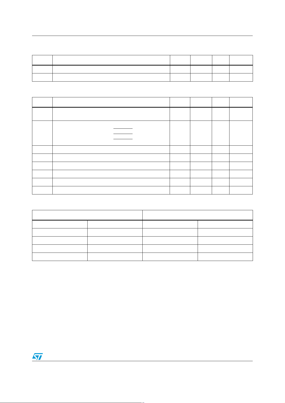
Figure 2. Standby position
VCC+
Standby
-
V
CC
To put the device in standby, a logic level must be applied on the standby MOS input. Since
ground is a virtual level for the device, the threshold voltage has been referred to V
V
-1.6 V typical.
CC+
CC+
at
In standby mode, the output goes into high impedance in 200 ns. Note that all maximum
ratings must still be followed in this mode. This mode leads to a swing limitation while using
the device in a signal multiplexing configuration with followers; the differential input voltage
must not exceed ±5 V, limiting the input swing to 2.5 Vpp.
6/19 Doc ID 5243 Rev 2

TSH95 Application information
4 Application information
Figure 3. Signal multiplexing
Figure 4. Sample and hold
4.1 Printed circuit layout recommendations
As with any high-frequency device, a few rules must be observed when designing the PCB
so as to maximize performance.
From the most to the least important points:
● Each power supply lead must be bypassed to ground with a 10 nF ceramic capacitor
and a 10 μF capacitor placed very close to the device.
● To provide low inductance and low resistance common return, use a ground plane or
common point return for power and signal.
● All leads must be wide and as short as possible, especially for the inputs, in order to
decrease parasitic capacitance and inductance.
● Use small resistor values to decrease the time constant with parasitic capacitance.
● Choose the smallest-possible component sizes (SMD).
● Decrease the capacitor load at the output to avoid degrading the circuit’s stability and
cause oscillation. You can also add a serial resistor to minimize its influence.
Doc ID 5243 Rev 2 7/19

Application information TSH95
Figure 5. Large signal follower response Figure 6. Static open-loop voltage gain
Figure 7. Input offset voltage drift versus
Figure 8. Small signal follower response
temperature
Figure 9. Closed-loop frequency response
Figure 10. Closed-lop frequency response
and phase shift
8/19 Doc ID 5243 Rev 2

TSH95 Application information
Figure 11. Audio bandwidth frequency
response & phase shift (TSH95 vs
standard 15 MHz audio op-amp)
Figure 13. Crosstalk isolation vs. frequency
(SO-16 package)
Figure 12. Gain flatness and phase shift vs.
frequency
Figure 14. Crosstalk isolation vs. frequency
(SO-16 package)
Figure 15. Input/output isolation in standby
mode (SO-16 package)
Doc ID 5243 Rev 2 9/19
Figure 16. Standby switching

Application information TSH95
Figure 17. Signal multiplexing Figure 18. Differential input impedance versus
frequency
4.5
4.0
3.5
3.0
)
W
2.5
2.0
Zin-diff (k
1.5
1.0
0.5
1k 10k 100k 1M 10M 100M
Frequency (Hz)
Figure 19. Common input impedance versus
frequency
120
100
80
)
W
60
Zin-com (M
40
20
1k 10k 100k 1M 10M 100M
Frequency (Hz)
10/19 Doc ID 5243 Rev 2

TSH95 Macromodel information
5 Macromodel information
The information below applies to the TSH95I.
** Standard Linear Ics Macromodels, 1996.
** CONNECTIONS :
* 1 INVERTING INPUT
* 2 NON-INVERTING INPUT
* 3 OUTPUT
* 4 POSITIVE POWER SUPPLY
* 5 NEGATIVE POWER SUPPLY
* 6 STANDBY
.SUBCKT TSH95 1 3 2 4 5 6 (analog)
********************************************************
**************** switch *******************
.SUBCKT SWITCH 20 10 IN OUT COM
.MODEL DIDEAL D N=0.1 IS=1E-08
DP IN 1 DIDEAL 400E-12
DN OUT 2 DIDEAL 400E-12
EP 1 OUT COM 10 2
EN 2 IN COM 10 2
RFUIT1 IN 1 1E+09
RFUIT2 OUT 2 1E+09
RCOM COM 0 1E+12
.ENDS SWITCH
**************** inverter *****************
.SUBCKT INV 20 10 IN OUT
.MODEL DIDEAL D N=0.1 IS=1E-08
RP1 20 15 1E+09
RN1 15 10 1E+09
RIN IN 10 1E+12
RIP IN 20 1E+12
DPINV OUT 20 DIDEAL 400E-12
DNINV 10 OUT DIDEAL 400E-12
GINV 0 OUT IN 15 -6.7E-7
CINV 0 OUT 210f
Doc ID 5243 Rev 2 11/19

Macromodel information TSH95
.ENDS INV
***************** AOP **********************
.MODEL MDTH D IS=1E-8 KF=1.809064E-15
CJO=10F
* INPUT STAGE
CIP 2 5 1.000000E-12
CIN 1 5 1.000000E-12
EIP 10 5 2 5 1
EIN 16 5 1 5 1
RIP 10 11 2.600000E-01
RIN 15 16 2.600000E-01
RIS 11 15 3.645298E-01
DIP 11 12 MDTH 400E-12
DIN 15 14 MDTH 400E-12
VOFP 12 13 DC 0.000000E+00
VOFN 1314DC 0
FPOL 13 5 VSTB 1E+03
CPS 11 15 2.986990E-10
DINN 17 13 MDTH 400E-12
VIN 17 5 2.000000e+00
DINR 15 18 MDTH 400E-12
VIP 4 18 1.000000E+00
FCP 4 5 VOFP 3.500000E+00
FCN 5 4 VOFN 3.500000E+00
ISTB0 4 5 130UA
FIBP 2 5 VOFP 1.000000E-02
FIBN 5 1 VOFN 1.000000E-02
* AMPLIFYING STAGE
FIP 5 19 VOFP 2.530000E+02
FIN 5 19 VOFN 2.530000E+02
RG1 19 120 3.160721E+03
XCOM1 4 0 120 5 COM SWITCH
RG2 19 121 3.160721E+03
12/19 Doc ID 5243 Rev 2

TSH95 Macromodel information
XCOM2 4 0 4 121 COM SWITCH
CC 19 5 2.00000E-09
DOPM 19 22 MDTH 400E-12
DONM 21 19 MDTH 400E-12
HOPM 22 28 VOUT 1.504000E+03
VIPM 28 4 5.000000E+01
HONM 21 27 VOUT 1.400000E+03
VINM 5 27 5.000000E+01
*********** ZP **********
RZP1 5 80 1E+06
RZP2 4 80 1E+06
GZP 5 82 19 80 2.5E-05
RZP2H 83 4 10000
RZP1H 83 82 80000
RZP2B 84 5 10000
RZP1B 82 84 80000
LZPH 4 83 3.535e-02
LZPB 84 5 3.535e-02
**************************
EOUT26 2382 51
VOUT 23 5 0
ROUT 26 103 35
COUT 103 5 30.000000E-12
XCOM 4 0 103 3 COM SWITCH
DOP 19 25 MDTH 400E-12
VOP 4 25 2.361965E+00
DON 24 19 MDTH 400E-12
VON 24 5 2.361965E+00
********** STAND BY ********
RMI1 4 111 1E+7
Doc ID 5243 Rev 2 13/19
Macromodel information TSH95
RMI2 0 111 2E+7
RONOFF 6 60 1K
CONOGG 60 0 10p
RSTBIN 60 0 1E+12
ESTBIN 106 0 6 0 1
ESTBREF 106 107 111 0 1
DSTB1 107 108 MDTH 400E-12
VSTB 108 109 0
ISTB 109 0 1U
RSTB 109 110 1
DSTB2 0 110 MDTH 400E-12
XINV 4 0 6 COM INV
.ENDS
Table 6. Electrical characteristics with VCC = ±5 V, T
amb
= 25° C
(unless otherwise specified)
Symbol Conditions Value Unit
V
io
A
I
CC
V
icm
V
V
I
sink
I
source
GBP R
SR R
φmR
RL = 600 Ω 3.2 V/mV
vd
No load/amplifier 5.2 mA
RL = 600 Ω +3.6 V
OH
RL = 600 Ω -3.6 V
OL
Vo = 0 V 40 mA
Vo = 0 V 40 mA
L
L
L
= 600 Ω, CL = 15 pF 147 MHz
= 600 Ω, CL = 15 pF 110 V/μs
= 600 Ω, CL = 15 pF 42 Degrees
0mV
-3 to 4 V
14/19 Doc ID 5243 Rev 2

TSH95 Package information
6 Package information
In order to meet environmental requirements, ST offers these devices in different grades of
ECOPACK
specifications, grade definitions and product status are available at: www.st.com.
ECOPACK
®
packages, depending on their level of environmental compliance. ECOPACK®
®
is an ST trademark.
Doc ID 5243 Rev 2 15/19

Package information TSH95
6.1 SO-16 package information
Figure 20. SO-16 package mechanical drawing
Table 7. SO-16 package mechanical data
Dimensions
Millimeters Inches
Ref.
Min. Typ. Max. Min. Typ. Max.
A1.750.069
A1 0.10 0.25 0.004 0.010
A2 1.25 0.049
b 0.31 0.51 0.012 0.020
c 0.17 0.25 0.007 0.010
(1)
D
9.80 9.90 10.00 0.386 0.390 0.394
E 5.80 6.00 6.20 0.228 0.236 0.244
E1
(2)
3.80 3.90 4.00 0.150 0.154 0.157
e 1.27 0.050
h 0.25 0.50 0.010 0.020
L 0.40 1.27 0.016 0.050
k0 8
ccc 0.10 0.004
1. Does not include mold flash, protrusions or gate burrs. Mold flash, protrusions or gate burrs not to exceed
0.15 mm in total.
2. Does not include interlead flash or protrusions. Interlead flash or protrusions not to exceed 0.25 mm per
side.
16/19 Doc ID 5243 Rev 2

TSH95 Ordering information
7 Ordering information
Table 8. Order codes
Part number
Temperature
range
Package Packing Marking
TSH95ID
TSH95IDT
TSH95IYD
TSH95IYDT
1. Qualification and characterization according to AEC Q100 and Q003 or equivalent, advanced screening
according to AEC Q001 & Q 002 or equivalent are on-going.
(1)
(1)
-40° C to +125° C
SO-16
(Automotive grade)
Tube or
Tape & reel
SO-16
TSH95I
TSH95IY
Doc ID 5243 Rev 2 17/19

Revision history TSH95
8 Revision history
Table 9. Document revision history
Date Revision Changes
01-Nov-2000 1 Initial release.
Document format updated.
27-Aug-2009 2
Updated SO-16 package information in Chapter 6.
Added automotive grade order codes in Tabl e 8 .
18/19 Doc ID 5243 Rev 2

TSH95
Please Read Carefully:
Information in this document is provided solely in connection with ST products. STMicroelectronics NV and its subsidiaries (“ST”) reserve the
right to make changes, corrections, modifications or improvements, to this document, and the products and services described herein at any
time, without notice.
All ST products are sold pursuant to ST’s terms and conditions of sale.
Purchasers are solely responsible for the choice, selection and use of the ST products and services described herein, and ST assumes no
liability whatsoever relating to the choice, selection or use of the ST products and services described herein.
No license, express or implied, by estoppel or otherwise, to any intellectual property rights is granted under this document. If any part of this
document refers to any third party products or services it shall not be deemed a license grant by ST for the use of such third party products
or services, or any intellectual property contained therein or considered as a warranty covering the use in any manner whatsoever of such
third party products or services or any intellectual property contained therein.
UNLESS OTHERWISE SET FORTH IN ST’S TERMS AND CONDITIONS OF SALE ST DISCLAIMS ANY EXPRESS OR IMPLIED
WARRANTY WITH RESPECT TO THE USE AND/OR SALE OF ST PRODUCTS INCLUDING WITHOUT LIMITATION IMPLIED
WARRANTIES OF MERCHANTABILITY, FITNESS FOR A PARTICULAR PURPOSE (AND THEIR EQUIVALENTS UNDER THE LAWS
OF ANY JURISDICTION), OR INFRINGEMENT OF ANY PATENT, COPYRIGHT OR OTHER INTELLECTUAL PROPERTY RIGHT.
UNLESS EXPRESSLY APPROVED IN WRITING BY AN AUTHORIZED ST REPRESENTATIVE, ST PRODUCTS ARE NOT
RECOMMENDED, AUTHORIZED OR WARRANTED FOR USE IN MILITARY, AIR CRAFT, SPACE, LIFE SAVING, OR LIFE SUSTAINING
APPLICATIONS, NOR IN PRODUCTS OR SYSTEMS WHERE FAILURE OR MALFUNCTION MAY RESULT IN PERSONAL INJURY,
DEATH, OR SEVERE PROPERTY OR ENVIRONMENTAL DAMAGE. ST PRODUCTS WHICH ARE NOT SPECIFIED AS "AUTOMOTIVE
GRADE" MAY ONLY BE USED IN AUTOMOTIVE APPLICATIONS AT USER’S OWN RISK.
Resale of ST products with provisions different from the statements and/or technical features set forth in this document shall immediately void
any warranty granted by ST for the ST product or service described herein and shall not create or extend in any manner whatsoever, any
liability of ST.
ST and the ST logo are trademarks or registered trademarks of ST in various countries.
Information in this document supersedes and replaces all information previously supplied.
The ST logo is a registered trademark of STMicroelectronics. All other names are the property of their respective owners.
© 2009 STMicroelectronics - All rights reserved
STMicroelectronics group of companies
Australia - Belgium - Brazil - Canada - China - Czech Republic - Finland - France - Germany - Hong Kong - India - Israel - Italy - Japan -
Malaysia - Malta - Morocco - Philippines - Singapore - Spain - Sweden - Switzerland - United Kingdom - United States of America
www.st.com
Doc ID 5243 Rev 2 19/19
 Loading...