

TSH341
300MHz Single Supply Video Amplifier with Low In/Out Rail
■ Bandwidth: 300MHz
■ Single supply operation down to 3V
■ Low input & output rail
■ Very low harmonic distortion
■ Slew rate: 400V/µs
■ Voltage Input noise: 7nV/√Hz
■ Specified for 150Ω load and 100Ω load
■ Tested on 5V power supply
■ Data min. and max. are tested during
production (Table 3)
Description
The TSH341 is a single supply operational
amplifier featurin g a large bandwidth of 300MHz
at unity gain for only 9.8mA of quiescent current.
An advantage of this circuit is its low input and
output rail feature wh ich is very close to GND in
single supply. This rail is tested and guaranteed
during production at 60mV (max.) from G ND on a
Ω load. This allows a good output swing which
150
fits perfectly when driving a video signal on a 75Ω
video line. Chapter 5 gives technical support
when using the TSH341 as a driver for video DAC
output on a video line . In particular, this chapter
focuses on applying a video signal DC shift to
avoid any clamping of the synchronization tip.
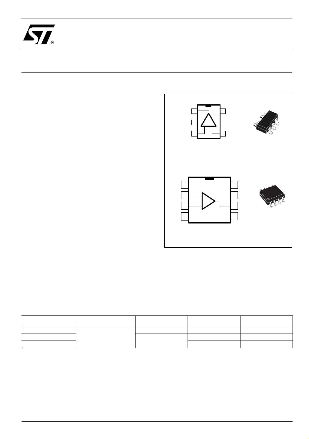
The TSH341 is available in the tiny SOT23-5 and
SO8 plastic packages.
Pin Connections (top view)
OUT
OUT
NC
NC
-IN
-IN
+IN
+IN
-VCC
-VCC
-VCC
-VCC
1
1
2
2
3
3
4
4
1
1
2
2
3
3
SOT23-5
SOT23-5
+ -
+ -
_
_
+
+
SO8
SO8
5
5
4
4
+VCC
+VCC
-IN+IN
-IN+IN
8
8
7
7
6
6
5
5
NC
NC
+VCC
+VCC
OUT
OUT
NC
NC
Applications
■ High-end video systems
■ High Definition TV (HDTV)
■ Broadcast video
■ Multimedia products
Order Codes
Part Number Temperature Range Package Packaging Marking
TSH341ILT
TSH341ID
TSH341IDT Tape & Reel H341I
March 2005 Revision 2 1/13
-40°C to +85°C
SOT23-5 Tape & Reel K307
SO-8
Tube H341I
TSH341 Absolute Maximum Ratings
1 Absolute Maximum Ratings
Table 1. Key parameters and their absolute maximum ratings
Symbol Parameter Value Unit
V
CC
Vid
V
in
T
oper
T
std
T
R
thjc
R
thja
P
max.
ESD
Supply voltage
Differential Input Voltage
Input Voltage Range
Operating Free Air Temperature Range
Storage Temperature
Maximum Junction Temperature
j
Thermal Resistance Junction to Case
SOT23-5
SO8
Thermal Resistance Junction to Ambient Area
SOT23-5
SO8
Maximum Power Dissipation (@Ta=25°C) for Tj=150°C
SOT23-5
SO8
CDM: Charged Device Model
HBM: Human Body Model
MM: Machine Model
Output Short Circuit
1
2
3
6V
+/-0.5 V
-0.2 to +3 V
-40 to +85 °C
-65 to +150 °C
150 °C
80
°C/W
28
250
°C/W
175
500
mW
715
2
1.5
200
4
kV
kV
V
1) All voltage values, except different ial voltage are with respect to network terminal.
2) Differential voltage are non-invert ing input terminal with respect to the inverting input terminal.
3) The magnitude of input and output voltage must never exceed VCC +0.3V.
4) An output current limitation protects the circuit from trans ient currents. Short-circuits can cause excessive heati ng.
Destructive dissipation can result from short circuit on amplifiers.
Table 2. Operating conditions
Symbol Parameter Value Unit
V
Power Supply Voltage
CC
Vicm Common Mode Input Voltage -0.4 to 3 V
1) Tested in full production at 0V/5V single power supply
3 to 5.5
1
V
2/13

Electrical Characteristics TSH341
2 Electrical Characteristics
Table 3. V
= +5V, T
CC
= 25°C (unless otherwise specified)
amb
Symbol Parameter Test Condition Min. Typ. Max. Unit
DC Performance
V
io
∆V
I
ib
A
VD
CMR
SVR
PSR
R
IN
C
IN
CC
I
Input Offset Voltage T
Vio drift vs. Temperature -40°C < T
io
Input Bias Current T
Open Loop Gain ∆V
Common Mode Rejection Ratio
20 log (∆V
icm
/∆Vio)
Supply Voltage Rejection Ratio
20 log (∆V
/∆Vio)
cc
Power Supply Rejection Ratio
/∆V
20 log (∆V
)
cc
out
Input Resistance
Input Capacitance
Total Supply Current No Load, V
, V
amb
-40°C < T
amb
-40°C < T
∆V
-40°C < T
∆V
-40°C < T
∆V
=0.6V
icm
< +85°C
amb
< +85°C
amb
, V
=0.6V
icm
< +85°C
amb
=2V, RL=150Ω
OUT
= 2V
icm
< +85°C
amb
=4V to 5V, V
cc
< +85°C
amb
=200mVp-p, F=1MHz
cc
=0.6V
icm
icm
=0.6V
-15 -3 15
-5
-30 µV/°C
616
7.2
70 100 dB
-60 -85
-83
-60 -85
-84
-77 dB
8.2 MΩ
3.5 pF
9.8 12.7 mA
Dynamic Performance and Output Characteristics
OUT
OUT
=0.6V,
icm
= 2Vp-p,
OUT
= 150Ω
L
< +85°C
=20mVp
=20mVp
300
90
150
MHz
65
70 100 MHz
400 V/µs
3.7 3.9 V
40 60 mV
70 100
90
Bw
FPBW
SR
V
OH
V
OL
I
OUT
-3dB Bandwidth Small Signal V
=0.6V, RL=150Ω
V
icm
Gain=+1
Gain=+2
Gain Flatness @ 0.1dB Small Signal V
Gain=+2, V
L=150Ω
R
Full Power Bandwidth V
icm
=2V, V
Gain=1, R
Slew Rate V
=2Vp-p, RL=150Ω,
OUT
Gain=+2,
High Level Output Voltage RL = 150Ω
Low Level Output Voltage RL = 150Ω
Output Short Circuit Current T
amb
-40°C < T
amb
Noise and Distortion
eN Equivalent Input Noise Voltage F = 100kHz 7 nV/√Hz
iN Equivalent Input Noise Current (+) F = 100kHz 1.5 pA/√Hz
HD2
HD3
2nd Harmonic Distortion V
3rd Harmonic Distortion V
= 2Vp-p, RL = 150Ω
OUT
Gain=+2, F= 10MHz,
= 2Vp-p, RL = 150Ω
OUT
Gain=+2, F= 10MHz,
-57 dBc
-63 dBc
mV
µA
dB
dB
mA
3/13

TSH341 Electrical Characteristics
Figure 1. Frequency response
16
14
12
10
8
6
4
2
0
-2
Gain (dB)
-4
-6
-8
-10
Vcc=5V
-12
Load=100
-14
SO8 and SOT23-5
-16
1M 10M 100M
Gain=+4
Gain=+2
Gain=+1
Ω or 150Ω
Frequency (Hz)
Figure 2. Gain flatness - SOT23-5L
6,4
6,2
6,0
5,8
5,6
5,4
Gain (dB )
5,2
5,0
4,8
Vcc=5V
Gain=+2
4,6
1M 10M 100M
Frequency (Hz)
Load=150Ω
Load=100Ω
Figure 4. Frequency response on capa-load
20
C=47pF
Ω
Riso=10
10
0
C=10pF
Riso=0
C=22pF
Ω
Riso=10
-10
Vcc=5V
Frequency Response (dB)
Gain=+2
Load=Riso + C//1k
-20
1M 10M 100M
Ω (to ground)
C=0 or
10pF
Riso=0
Frequency (Hz)
Figure 5. Gain flatness - SO8
6,4
6,2
6,0
5,8
5,6
5,4
Gain (dB)
5,2
5,0
4,8
Vcc=5V
4,6
1M 10M 100M
Load=100Ω
Frequency (Hz)
Load=150Ω
Figure 3. T otal input noise vs. frequency
non-inverting input in short-circuit
Vcc=5V
100
Input Noise (nV/VHz)
10
100 1k 10k 100k 1M 10M
Frequency (Hz)
4/13
Figure 6. Positive and negative slew rate
3,0
Vcc=5V
G=+2
2,5
Load=100
Ω or 150Ω
2,0
1,5
1,0
SR-
Output Response (V)
0,5
0,0
-5ns -4ns -3ns -2ns -1ns 0s 1ns 2ns 3ns 4ns 5ns
Time
SR+
 Loading...