

Ultra low power video buffer/filter with power-down
Features
■ Very low consumption: 1.7 mA
■ Ultra low power-down mode: 4 nA typ.,
500 nA max.
■ Internal 6
■ Internal gain of 6 dB
■ Rail-to-rail output buffer for 75 Ω video line
■ Excellent video performance
– Differential gain 0.5%
– Differential phase 0.10°
– Group delay of 10 ns
■ SAG correction
■ Bottom of video signal close to 0 V
■ Tested with 2.5 V and 3.3 V single supply
■ Data min. and max. are physically tested and
guaranteed during production (consumption,
gain, filtering, and other parameters are
guaranteed)
th
order reconstruction filter
IN
IN
GND
GND
SAG
SAG
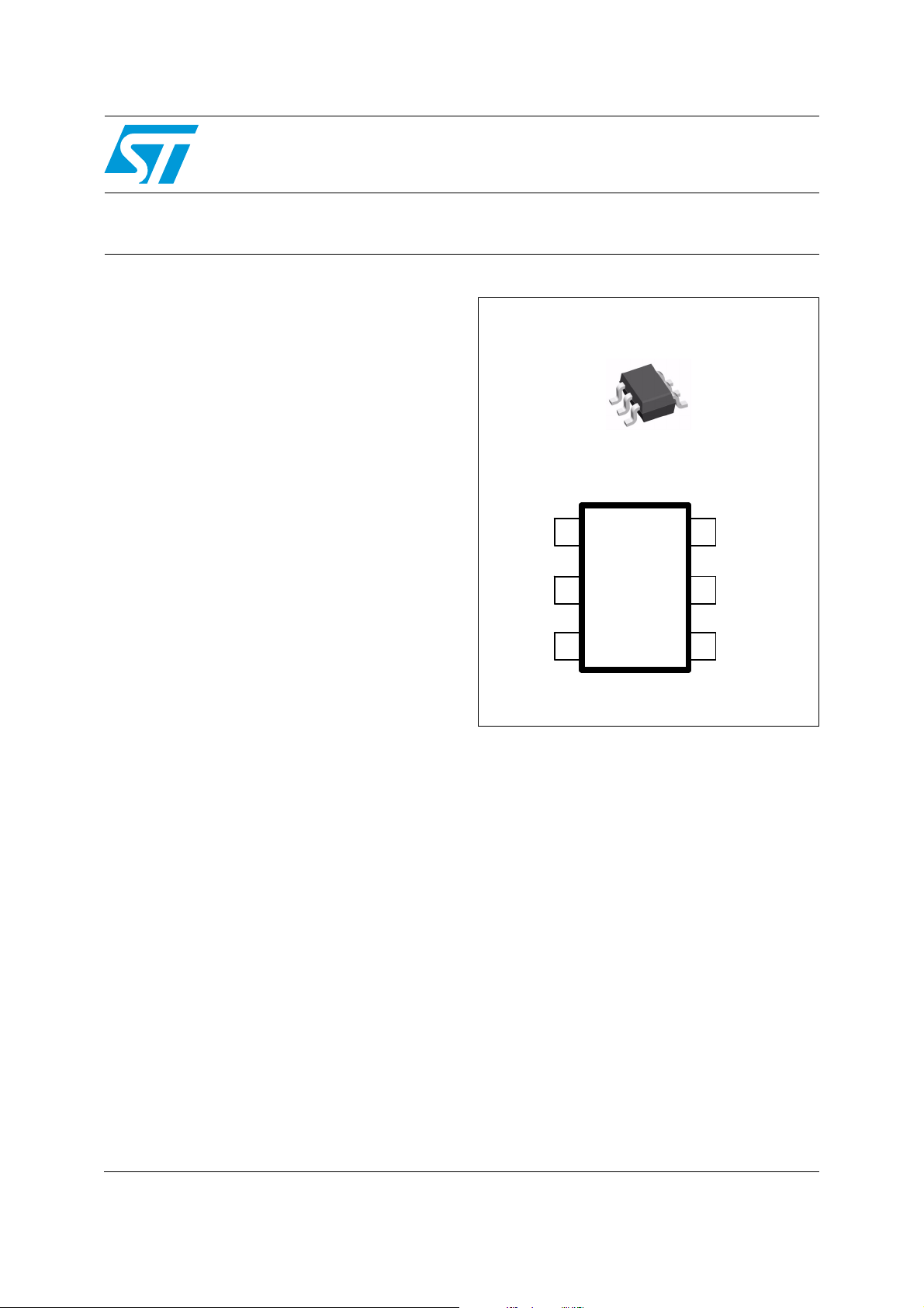
TSH122
SC70
Top view
Top view
6
1
1
2
2
3
3
6
Vcc
Vcc
EN (enable)
EN (enable)
5
5
OUT
OUT
4
4
Applications
Description
■ Mobile phones
■ Digital still camera
■ Digital video camera
■ Portable DVD players
August 2008 Rev 1 1/16
The TSH122 is a video buffer that uses a voltage
feedback amplifier, with an internal gain of 6 dB,
an output rail-to-rail, an internal input DC-shift and
a SAG correction. A power-down function allows
switching to a sleep mode with an ultra-low
consumption.
The TSH122 features a 6th-order internal
reconstruction filter to attenuate the parasitic
frequency of 27 MHz from the clock of the video
DAC.
The TSH122 operates from 2.25 to 5 V single
power supplies and is tested at 2.5 V and 3.3 V.
The TSH122 is a single operator available in a
tiny SC70 plastic package for space saving.
www.st.com
16
Absolute maximum ratings and operating conditions TSH122
1 Absolute maximum ratings and operating conditions
Table 1. Absolute maximum ratings
Symbol Parameter Value Unit
V
CC
V
T
T
R
thja
R
thjc
Supply voltage
Maximum input amplitude 0 to Vcc V
in
Storage temperature -65 to +150 °C
stg
Maximum junction temperature 150 °C
j
SC70 thermal resistance junction to ambient area 205 °C/W
SC70 thermal resistance junction to case 172 °C/W
Maximum power dissipation for Tj=150°C
P
max
T
T
amb
amb
= +25°C
= +85°C
CDM: charged device model
ESD
HBM: human body model
MM: machine model
Output short-circuit
1. All voltage values, except differential voltage, are with respect to network terminal.
2. Charged device model: all pins and the package are charged together to the specified voltage and then
discharged directly to the ground through only one pin. This is done for all pins.
3. Human body model: a 100 pF capacitor is charged to the specified voltage, then discharged through a
1.5 kΩ resistor between two pins of the device. This is done for all couples of connected pin combinations
while the other pins are floating.
4. Machine model: a 200 pF capacitor is charged to the specified voltage, then discharged directly between
two pins of the device with no external series resistor (internal resistor < 5 Ω). This is done for all couples of
connected pin combinations while the other pins are floating
5. An output current limitation protects the circuit from transient currents. Short-circuits can cause excessive
heating. Destructive dissipation can result from short-circuits on amplifiers.
Table 2. Operating conditions
(1)
(4)
(3)
(2)
5.5 V
609
mW
317
1.5
1.5
300
(5)
kV
kV
V
Symbol Parameter Value Unit
V
CC
T
oper
1. Tested in full production at 0 V/2.5 V and 0 V/3.3 V single power supply.
Power supply voltage 2.25 to 5
Operating free air temperature range -40 to +85 °C
2/16
(1)
V
TSH122 Electrical characteristics
2 Electrical characteristics
Table 3. VCC = +2.5V, +3.3V, T
= 25°C (unless otherwise specified)
amb
Symbol Parameter Test conditions Min. Typ. Max. Unit
DC performance
V
I
Output DC level shift RL = 150Ω 70 115 168 mV
dc
= +3.3V -1.5 -0.87
V
CC
Input bias current
ib
V
T
min
= +3.3V,
CC
≤ T
amb
≤ T
max
-0.93
Vin=0V to 1V DC, VCC=+2.5V 5.8 6 6.1
=0V to 1.4V DC, VCC=+3.3V 5.8 6 6.1
V
G Internal voltage gain
PSRR
I
CC
Power supply rejection ratio
20 log (ΔV
CC
/ΔV
Positive supply current
DC consumption
out
)
in
=3.3V
V
CC
≤ T
T
ΔV
min
CC
≤ T
amb
=±100mV at 1kHz
Vin=+0.5V DC
=0V, no load
V
in
=+3.3V
V
CC
VCC=+2.5V
=+3.3V
V
CC
≤ T
T
min
amb
≤ T
max
max
5.96
55 dB
2
1.7
2.4
2.1
2.4 mA
Dynamic performance and output characteristics
μA
dB
mA
Small signal
V
=+3.3V, RL = 150Ω
CC
BW Filter bandwidth
-3dB bandwidth
-1dB bandwidth 5.4
9.5
7.2
MHz
-1dB bandwidth
FR 27 MHz rejection
= +3.3V,
V
CC
T
≤ T
amb
≤ T
min
Small signal
V
=+3.3V, RL=150Ω
CC
= +3.3V,
V
CC
≤ T
T
min
amb
≤ T
max
max
6.75
36 47 dB
46 dB
ΔG Differential gain VCC=+3.3V, RL=150Ω 0.5 %
ΔΦ Differential phase V
Gd Group delay V
V
High level output voltage
OH
=+3.3V, RL=150Ω 0.1 °
CC
=+3.3V, 10kHz-5MHz 6 ns
CC
V
=+3.3V, RL=150Ω
CC
VCC=+2.5V, RL=150Ω
3.1
2.3
3.2
2.4
V
3/16
Electrical characteristics TSH122
Table 3. VCC = +2.5V, +3.3V, T
= 25°C (unless otherwise specified) (continued)
amb
Symbol Parameter Test conditions Min. Typ. Max. Unit
V
I
out
Low level output voltage RL = 150Ω 11 40 mV
OL
Output short circuit current VCC=+2.5V 75 mA
Noise and distortion
eN Total output noise F = 100kHz, no load 51 nV/√Hz
=+3.3V, RL = 150Ω
V
CC
=1V
HD Harmonic distortion
V
H2
H3
in
, F=1MHz
p-p
64
61
Enable/power-down
Low level on pin-5: TSH122 in power-down
High level on pin-5: TSH122 enabled
I
V
V
high
T
T
Consumption in power-down
sd
mode
Low-level threshold 0 +0.3 V
low
High-level threshold +0.7
Time from power-down to enable 1 μs
on
Time from enable to power-down 1 μs
off
=+3.3V 4 500 nA
V
CC
V
CC
dBc
V
4/16
TSH122 Electrical characteristics
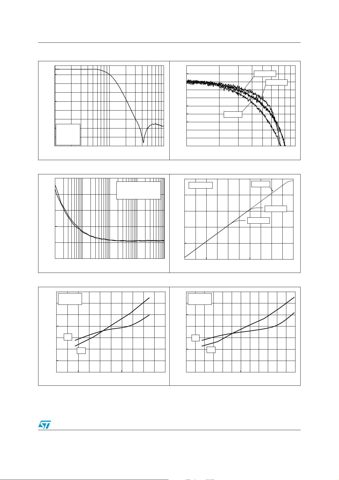
Figure 1. Frequency response Figure 2. Gain flatness
10
0
-10
-20
-30
-40
Gain (dB)
-50
Vcc=3.3V
-60
Load=150
-70
Small signal
Vicm=0.5V
-80
1M 10M 100M
Ω
Frequency (Hz)
6.2
6.1
6.0
5.9
5.8
5.7
5.6
Flatness (dB)
5.5
5.4
5.3
5.2
1M 10M
Vcc=+5V
Frequency (Hz)
Figure 3. Input noise Figure 4. Distortion
250
200
150
No load
Input to GND
Vcc=+2.5V and +3.3V
5
Load=150Ω
4
3
Vcc=+2.5V
Vcc=+3.3V
Vcc=+5V
Vcc=+3.3V
100
(nV/VHz)
n
e
50
0
100 1k 10k 100k 1M
Frequency (Hz)
2
Vout (V)
1
0
0.0 0.5 1.0 1.5 2.0 2.5
Vin (V)
Figure 5. Distortion at Vcc=2.5 V Figure 6. Distortion at Vcc=3.3 V
Vcc=+2.5V
-30
Vcc=2.5V
Load=150
-40
-50
-60
-70
Distortion (dB)
-80
-90
-100
0.0 0.5 1.0 1.5 2.0 2.5
Ω
H2
H3
Output Amplitude (Vp-p)
-30
Vcc=3.3V
Load=150
-40
-50
-60
-70
Distortion (dB)
-80
-90
-100
0.0 0.5 1.0 1.5 2.0 2.5 3.0
Ω
H2
H3
Output Amplitude (Vp-p)
5/16

Electrical characteristics TSH122
Figure 7. DCshift vs. Vcc Figure 8. VOL vs. Vcc
125
124
123
122
121
120
119
118
Output DCshift (mV)
117
116
115
2.0 2.5 3.0 3.5 4 .0 4.5 5.0
Load=150Ω
Vcc (V)
10
9
8
7
6
5
4
VOL (mV)
3
2
Vin= -100mV
1
Load=150
0
2345
Ω
Figure 9. Icc vs. Vcc Figure 10. Power down
4.0
3.5
3.0
2.5
2.00
1.75
1.50
Vcc (V)
2.0
Icc (mA)
1.5
1.0
0.5
0.0
0123456
Vcc (V)
1.25
Isd (nA)
1.00
0.75
0.50
2.02.53.03.54.04.55.05.5
Vcc (V)
Figure 11. Switch-on output settling Figure 12. Switch-off output settling
EN (pin5)
EN (pin5)
Vout (pin4)
Vout (pin4)
Vcc=+3.3V, Vin=+1.3Vdc
Vcc=+3.3V, Vin=+1.3Vdc
6/16

TSH122 Electrical characteristics
Figure 13. In/Out switch on/off Figure 14. Synchronization tip at 0 V
Vin
V
in
Vout
V
out
EN (pin5)
Vcc=+3.3V
Vcc=+3.3V
Figure 15. VOL vs. temperature Figure 16. VOH vs. temperature
20.0
17.5
15.0
12.5
10.0
7.5
VOL (mV)
5.0
2.5
Load=150Ω
0.0
-40 -20 0 20 40 60 80
Vcc=+2.5V
Vcc=+3.3V
Temperature (°C)
5.0
Load=150Ω
4.5
4.0
3.5
VOH (mV)
3.0
2.5
Vcc=+3.3V
Vcc=+2.5V
2.0
-40-20 0 20406080
Temperature (°C)
Figure 17. Bandwidth vs. temperature Figure 18. Attenuation vs. temperature
9.0
8.5
8.0
7.5
7.0
6.5
6.0
5.5
Bw@-1dB (MHz)
5.0
Small signal
4.5
Load=150
4.0
-40-20 0 20406080
Vcc=+2.5V
Vcc=+3.3V
Ω
Temperature (°C)
-40.0
-42.5
Vcc=+2.5V
-45.0
-47.5
-50.0
-52.5
-55.0
Attenuation@27MHz (dB)
-57.5
Load=150Ω
-60.0
-40-20 0 20406080
Vcc=+3.3V
Temperature (°C)
7/16

Electrical characteristics TSH122
Figure 19. Icc vs. temperature Figure 20. Gain vs. temperature
3.0
2.5
Vcc=+3.3V
2.0
1.5
(mA)
CC
I
1.0
0.5
Vcc=+2.5V
no Load
0.0
-40 -20 0 20 40 60 80
Temperature (°C)
6.10
6.05
Vcc=+3.3V
6.00
Gain (dB)
Vcc=+2.5V
5.95
Load=150Ω
5.90
-40-20 0 20406080
Temperature (°C)
Figure 21. Output DC shift vs. temperature Figure 22. Ibias vs. temperature
200
Vcc=+2.5V and +3.3V
180
Load=150
160
140
120
100
80
60
Output DCshift (mV)
40
20
0
-40-20 0 20406080
Ω
Temperature (°C)
0.00
-0.25
-0.50
-0.75
-1.00
(μA)
BIAS
I
-1.25
-1.50
-1.75
Load=150Ω
-2.00
-40 -20 0 20 40 60 80
Vcc=+2.5V
Vcc=+3.3V
Temperature (°C)
8/16

TSH122 Application information
3 Application information
3.1 Power supply considerations
Correct power supply bypassing is very important for optimizing performance in
high-frequency ranges. The bypass capacitors should be placed as close as possible to the
IC pins to improve high-frequency bypassing. A capacitor greater than 10 µF is necessary to
minimize the distortion. For better quality bypassing, we recommend adding a 10 nF
capacitor, also placed as close as possible to the IC pins.
Figure 23. Circuit for power supply bypassing
Figure 24. Supply noise rejection
10
Vcc=5V(dc)+0.2Vp-p(ac)
0
Load=150
Bypass capacitors: 10µF+10nF
-10
Ω
6##
43(
M&
N&
-20
-30
-40
-50
-60
Noise supply rejection (dB)
-70
-80
10k 100k 1M 10M 100M
Frequency (Hz)
9/16

Application information TSH122
3.2 Implementation considerations
3.2.1 Input
The DC level shifter optimizes the position of the video signal with no clamping on the output
rails.
3.2.2 Filter
A reconstruction filter is used to attenuate the DAC’s sampling frequency because it
generates a parasitic signal in the video spectrum (typically at 27 MHz in the case of
standard video). This function is fulfilled while keeping a low group delay and a good gain
flatness along the video band.
Figure 25. Internal schematic
2.25 V to 5 V
2.25 V to 5 V
+Vcc
+Vcc
6
DC shifter
DC shifter
6
Power-down
Power-down
5
5
3.2.3 Output
In an AC-coupling configuration, the SAG correction allows use of two small low-cost
capacitors in place of one large capacitor (see Figure 26). The AC-coupling output reduces
the power consumption by removing the DC component included in the signal.
Nevertheless, the output can be directly connected to the line without any capacitor. In this
case, the OUT and SAG pins are connected together and the equivalent gain of the buffer
remains at 6 dB (see Figure 27).
Input
Input
1
1
LPF
6
6
LPF
th
th
order
order
2R
2R
+
+
+
+
Output
Output
4
4
-
-
2
2
GND
GND
2R
2R
R
R
2R
2R
3
3
SAG
SAG
10/16

TSH122 Application information
Figure 26. Schematic diagram with output capacitor
6TO6
46
6IDEO
$!#
$!#S
LOAD
0OWERDOWN
3!'
&
&
%QUIVALENTTOASINGLE
!#COUPLINGOUTPUTWITH
ABIGCAPACITOROF&
&
7
7
7 CABLE
7
7 CABLE
7
Figure 27. Schematic diagram without output capacitor
6TO6
6IDEO
$!#
$!#S
LOAD
0OWERDOWN
3!'
7
46
7 CABLE
7
11/16

Application information TSH122
3.3 Using the TSH122 to drive a Cvbs signal
Figure 28. Details on Cvbs (NTSC color bar 100%)
DAC output amplitude
DAC output amplitude
~1.3 V
+133 IRE
+133 IRE
+100 IRE
+100 IRE
0 IRE
0 IRE
-40 IRE
-40 IRE
~1.3 V
White
White
Blanking
Blanking
GND
GND
level
level
Burst
Burst
Synchronization tip
Synchronization tip
With its internal DC shift, the TSH122 can drive a video signal from the DAC output as low
as 0 V (bottom of the synchronization tip at 0 V - see Figure 14).
12/16

TSH122 Package information
4 Package information
In order to meet environmental requirements, STMicroelectronics offers these devices in
ECOPACK
®
packages. These packages have a lead-free second level interconnect. The
category of second level interconnect is marked on the package and on the inner box label,
in compliance with JEDEC Standard JESD97. The maximum ratings related to soldering
conditions are also marked on the inner box label. ECOPACK is an STMicroelectronics
trademark. ECOPACK specifications are available at: www.st.com
.
Figure 29. SC70-6 (or SOT323-6) package footprint (in millimeters)
0.65
1.05
0.80
2.90
0.40
13/16

Package information TSH122
Figure 30. SC70-6 (or SOT323-6) package mechanical data
Dimensions
Ref
Min Typ Max Min Typ Max
A 0.80 1.10 31.5 43.3
A1 00.100 3.9
A2 0.80 1.00 31.5 39.3
b 0.15 0.30 5.9 11.8
c 0.10 0.18 3.9 7.0
D 1.80 2.20 70.8 86.6
E 1.15 1.35 45.2 43.1
e 0.65 25.6
HE 1.8 2.4 70.8 94.5
L 0.10 0.40 3.9 15.7
Q1 0.10 0.40 3.9 15.7
Millimeters Mils
Q1
A1
C
A
A2
D
b
L
HE
E
ee
14/16

TSH122 Ordering information
5 Ordering information
Table 4. Order codes
Part number Temperature range Package Packaging Marking
TSH122ICT -40°C to +85°C SC70 Tape & reel K31
6 Revision history
Table 5. Document revision history
Date Revision Changes
04-Aug-2008 1 Initial release.
15/16

TSH122
Please Read Carefully:
Information in this document is provided solely in connection with ST products. STMicroelectronics NV and its subsidiaries (“ST”) reserve the
right to make changes, corrections, modifications or improvements, to this document, and the products and services described herein at any
time, without notice.
All ST products are sold pursuant to ST’s terms and conditions of sale.
Purchasers are solely responsible for the choice, selection and use of the ST products and services described herein, and ST assumes no
liability whatsoever relating to the choice, selection or use of the ST products and services described herein.
No license, express or implied, by estoppel or otherwise, to any intellectual property rights is granted under this document. If any part of this
document refers to any third party products or services it shall not be deemed a license grant by ST for the use of such third party products
or services, or any intellectual property contained therein or considered as a warranty covering the use in any manner whatsoever of such
third party products or services or any intellectual property contained therein.
UNLESS OTHERWISE SET FORTH IN ST’S TERMS AND CONDITIONS OF SALE ST DISCLAIMS ANY EXPRESS OR IMPLIED
WARRANTY WITH RESPECT TO THE USE AND/OR SALE OF ST PRODUCTS INCLUDING WITHOUT LIMITATION IMPLIED
WARRANTIES OF MERCHANTABILITY, FITNESS FOR A PARTICULAR PURPOSE (AND THEIR EQUIVALENTS UNDER THE LAWS
OF ANY JURISDICTION), OR INFRINGEMENT OF ANY PATENT, COPYRIGHT OR OTHER INTELLECTUAL PROPERTY RIGHT.
UNLESS EXPRESSLY APPROVED IN WRITING BY AN AUTHORIZED ST REPRESENTATIVE, ST PRODUCTS ARE NOT
RECOMMENDED, AUTHORIZED OR WARRANTED FOR USE IN MILITARY, AIR CRAFT, SPACE, LIFE SAVING, OR LIFE SUSTAINING
APPLICATIONS, NOR IN PRODUCTS OR SYSTEMS WHERE FAILURE OR MALFUNCTION MAY RESULT IN PERSONAL INJURY,
DEATH, OR SEVERE PROPERTY OR ENVIRONMENTAL DAMAGE. ST PRODUCTS WHICH ARE NOT SPECIFIED AS "AUTOMOTIVE
GRADE" MAY ONLY BE USED IN AUTOMOTIVE APPLICATIONS AT USER’S OWN RISK.
Resale of ST products with provisions different from the statements and/or technical features set forth in this document shall immediately void
any warranty granted by ST for the ST product or service described herein and shall not create or extend in any manner whatsoever, any
liability of ST.
ST and the ST logo are trademarks or registered trademarks of ST in various countries.
Information in this document supersedes and replaces all information previously supplied.
The ST logo is a registered trademark of STMicroelectronics. All other names are the property of their respective owners.
© 2008 STMicroelectronics - All rights reserved
STMicroelectronics group of companies
Australia - Belgium - Brazil - Canada - China - Czech Republic - Finland - France - Germany - Hong Kong - India - Israel - Italy - Japan -
Malaysia - Malta - Morocco - Singapore - Spain - Sweden - Switzerland - United Kingdom - United States of America
www.st.com
16/16
 Loading...