

ST TSH110, TSH111, TSH112, TSH113, TSH114 User Manual
TSH110-TSH111-TSH112-TSH113-TSH114
Wide band low noise operational amplifiers
Features
● Low noise: 3nV/√Hz
● Low supply current: 3.2mA
● 47mA output current
● Bandwidth: 100MHz
● 5V to 12V supply voltage
● Slew rate: 450V/μs
● Specified for 100Ω load
● Very low distortion
● Tiny SOT23-5, TSSOP and SO packages
Applications
● High-end video drivers
● Receiver for xDSL
● A/D converter driver
● High-end audio applications
Description
The single TSH110 and TSH111, the dual
TSH112, the triple TSH113 and the quad TSH114
are current feedback operational amplifiers
featuring a very high slew rate of 450V/µs and a
large bandwidth of 100MHz, with only a 3.2mA
quiescent supply current. The TSH111 and
TSH113 feature a Standby function for each
operator. This function is a power-down mode
with a high output impedance.
These devices operate from ±2.5V to ±6V dual
supply voltage or from 5V to 12V single supply
voltage. They are able to drive a 100Ω load with a
swing of 9V minimum (for a 12V power supply).
The harmonic and intermodulation distortions of
these devices are very low, making this circuit a
good choice for applications requiring wide
bandwidth with multiple carriers.
For board space and weight saving, the TSH110
comes in miniature SOT23-5 package.
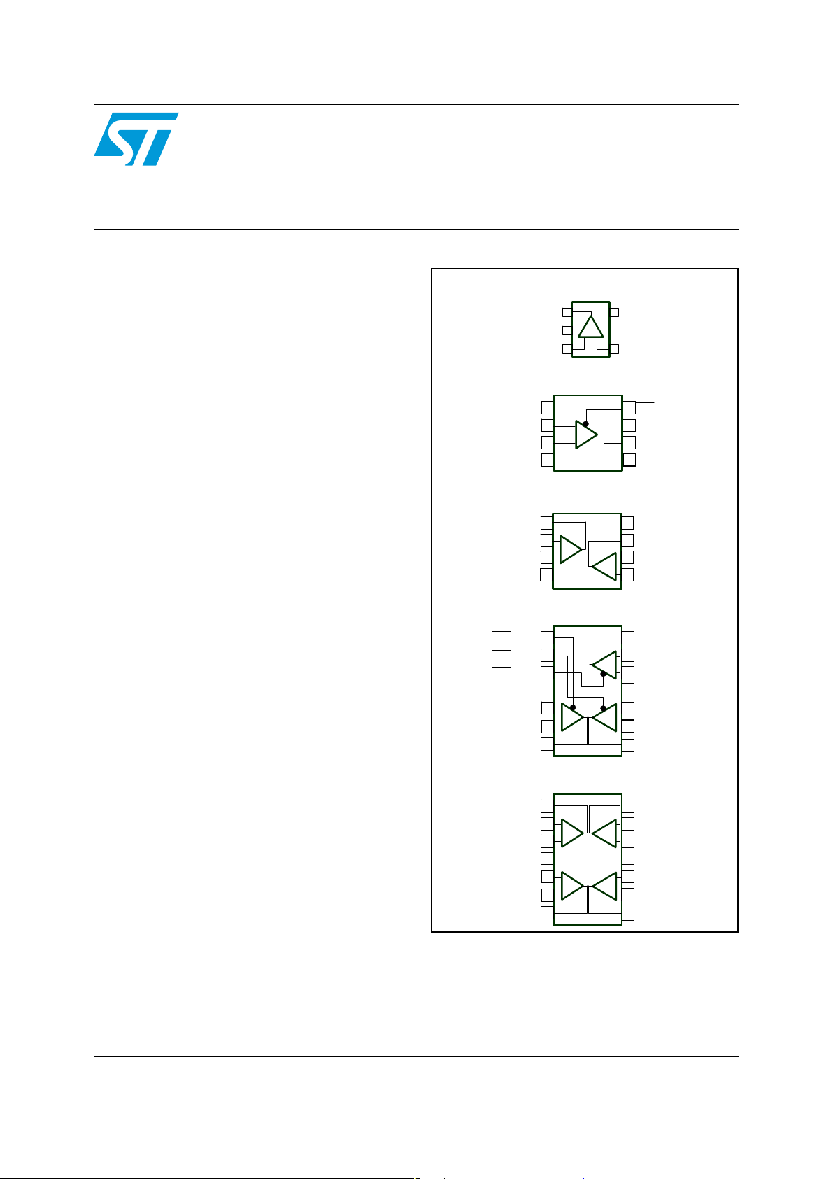
TSH110: SOT23-5
TSH110: SOT23-5
Output
Output
1
1
VCC -
VCC -
2
2
Non Inverting Input Inverting Input
Non Inverting Input Inverting Input
TSH111: SO-8/TSSOP8
TSH111: SO-8/TSSOP8
TSH111: SO-8/TSSOP8
Inverting Input
Inverting Input
Inverting Input
Non Inverting Input
Non Inverting Input
Non Inverting Input
VCC -
VCC -
VCC -
TSH112: SO-8/TSSOP8
TSH112: SO-8/TSSOP8
TSH112: SO-8/TSSOP8
Output1
Output1
Output1
Inverting Input1 Output2
Inverting Input1 Output2
Inverting Input1 Output2
Non Inverting Input1
Non Inverting Input1
Non Inverting Input1
VCC -
VCC -
VCC -
TSH113: SO-14/TSSOP14
TSH113: SO-14/TSSOP14
TSH113: SO-14/TSSOP14
STANDBY1
STANDBY1
STANDBY1
STANDBY2
STANDBY2
STANDBY2
STANDBY3
STANDBY3
STANDBY3
VCC +
VCC +
VCC +
Non Inverting Input1
Non Inverting Input1
Non Inverting Input1
Inverting Input1
Inverting Input1
Inverting Input1
Output1
Output1
Output1
TSH114: SO-14/TSSOP14
TSH114: SO-14/TSSOP14
TSH114: SO-14/TSSOP14
Output1
Output1
Output1
Inverting Input1
Inverting Input1
Inverting Input1
Non Inverting Input1
Non Inverting Input1
Non Inverting Input1
VCC +
VCC +
VCC +
Non Inverting Input2
Non Inverting Input2
Non Inverting Input2
Inverting Input2
Inverting Input2
Inverting Input2
Output2
Output2
Output2
NC
NC
NC
3
3
1
1
1
2
2
2
3
3
3
4
4
4
1
1
1
2
2
2
_
_
_
+
+
+
3
3
3
4
4
4
1
1
1
2
2
2
3
3
3
4
4
4
5
5
5
+
+
+
_
_
_
6
6
6
7
7
7
1
1
1
2
2
2
_
_
_
+
+
+
3
3
3
4
4
4
5
5
5
+
+
+
_
_
_
6
6
6
7
7
7
5
5
VCC +
VCC +
+ -
+ -
4
4
8
8
8
STANDBY
STANDBY
STANDBY
_
_
_
+
+
+
7
7
7
VCC +
VCC +
VCC +
Output
Output
Output
6
6
6
NC
NC
NC
5
5
5
VCC +
VCC +
VCC +
8
8
8
7
7
7
Inverting Input2
Inverting Input2
Inverting Input2
6
6
6
_
_
_
+
+
+
Non Inverting Input2
Non Inverting Input2
Non Inverting Input2
5
5
5
14
14
14
Output3
Output3
Output3
13
13
13
Inverting Input3
Inverting Input3
Inverting Input3
_
_
_
+
+
+
Non Inverting Input3
Non Inverting Input3
Non Inverting Input3
12
12
12
VCC -
VCC -
VCC -
11
11
11
10
10
10
Non Inverting Input2
Non Inverting Input2
Non Inverting Input2
+
+
+
_
_
_
Inverting Input2
Inverting Input2
Inverting Input2
9
9
9
Output2
Output2
Output2
8
8
8
14
14
14
Output4
Output4
Output4
13
13
13
Inverting Input4
Inverting Input4
Inverting Input4
_
_
_
+
+
+
Non Inverting Input4
Non Inverting Input4
Non Inverting Input4
12
12
12
11
11
11
VCC -
VCC -
VCC -
10
10
10
Non Inverting Input3
Non Inverting Input3
Non Inverting Input3
+
+
+
_
_
_
Inverting Input3
Inverting Input3
Inverting Input3
9
9
9
Output3
Output3
Output3
8
8
8
The TSH111 comes in SO-8 and TSSOP8
packages, the TSH112 comes in SO-8 and
TSSOP8 packages, the TSH113 and TSH114
come in SO-14 and TSSOP14 packages.
October 2007 Rev 2 1/15
www.st.com
15
Absolute maximum ratings and operating conditions TSH110-TSH111-TSH112-TSH113-TSH114
1 Absolute maximum ratings and operating conditions
Table 1. Absolute maximum ratings (AMR
Symbol Parameter Value Unit
(3)
(1)
(2)
14 V
±1 V
±6 V
80
28
22
°C/W
37
32
V
T
T
R
CC
V
V
oper
stg
T
thjc
Supply voltage
id
Differential input voltage
Input voltage
i
Operating free air temperature range -40 to +85 °C
Storage temperature -65 to +150 °C
Maximum junction temperature 150 °C
j
Thermal resistance junction to case
SOT23-5
SO-8
SO-14
TSSOP8
TSSOP14
Thermal resistance junction to ambiant area
SOT23-5
R
thja
SO-8
SO-14
TSSOP8
TSSOP14
HBM: human body model
ESD
CDM: charged device model
Output short circuit duration
1. All voltage values, except differential voltage, are with respect to network ground terminal.
2. Differential voltages are the non-inverting input terminal with respect to the inverting terminal.
3. The magnitude of input and output voltages must never exceed VCC +0.3V
4. Human body model: A 100pF capacitor is charged to the specified voltage, then discharged through a
1.5kΩ resistor between two pins of the device. This is done for all couples of connected pin combinations
while the other pins are floating.
5. Machine model: A 200pF capacitor is charged to the specified voltage, then discharged directly between
two pins of the device with no external series resistor (internal resistor < 5Ω). This is done for all couples of
connected pin combinations while the other pins are floating.
6. Charged device model: all pins and the package are charged together to the specified voltage and then
discharged directly to the ground through only one pin. This is done for all pins.
7. Short-circuits can cause excessive heating and can result in destructive dissipation.
Table 2. Operating conditions
(4)
(5)
(6)
(7)
250
157
125
130
110
2.0
0.2
1.5
°C/W
kVMM: machine model
Symbol Parameter Value Unit
V
CC
V
icm
Supply voltage 5 to 12 V
Common mode input voltage range V
2/15
-
+1.5 to V
CC
+
-1.5 V
CC

TSH110-TSH111-TSH112-TSH113-TSH114 Electrical characteristics
2 Electrical characteristics
Table 3. Dual supply voltage, VCC= ±2.5V, R
(1)
fb
= 680Ω, T
= 25°C (unless otherwise
amb
specified)
Symbol Parameter Test conditions Min. Typ. Max. Unit
DC performance
V
Input offset voltage
io
ΔV
R
CMR
SVR
PSR
Input offset voltage drift vs. temperature T
io
I
Non inverting input bias current
ib+
I
Inverting input bias current
ib-
Transimpedance RL=100Ω 500 750 kΩ
OL
I
Supply current per operator
CC
Common mode rejection ratio
ΔV
/ΔVio)
(
ic
Supply voltage rejection ratio
(
ΔV
/ΔVio)
CC
Power supply rejection ratio
ΔV
/ΔV
(
CC
out
)
Dynamic performance and output characteristics
T
amb
T
< T
min
min
T
amb
T
min
T
amb
T
min
T
amb
T
min
Gain=1, R
< T
< T
< T
< T
amb
amb
amb
amb
< T
< T
< T
max
max
max
max
3.2 4 mA
< T
< T
amb
max
=3.9kΩ 48 dB
load
-1.5 0.3 2.0 mV
1mV
5 μV/°C
-10 1.4 13 μA
2.5 μA
-3 1.9 7 μA
2.5 μA
3.5 mA
56 60 dB
70 80 dB
V
High level output voltage
oh
Low level output voltage
V
ol
| I
| Output sink current T
sink
I
source
Output source current T
BW -3dB bandwidth
SR Slew rate
T
amb
RL = 100Ω
T
< T
amb
< T
min
RL = 100Ω GND
T
amb
RL = 100Ω
< T
T
min
amb
< T
RL = 100Ω
< T
< T
amb
amb
< T
< T
fb
min
min
V
out
=1Vpk, R
max
max
max
max
(1)
=820Ω//2pF
1.4 2 V
1.9 V
-1.8 -1.3 V
-1.7 V
20 mA
18 mA
Load=100Ω
=+2 81 MHz
A
VCL
A
=+2, 2V step
VCL
Load=100Ω
160 230 V/μs
3/15

Electrical characteristics TSH110-TSH111-TSH112-TSH113-TSH114
Table 3. Dual supply voltage, VCC= ±2.5V, R
(1)
fb
= 680Ω, T
= 25°C (unless otherwise
amb
specified) (continued)
Symbol Parameter Test conditions Min. Typ. Max. Unit
T
Rise time
r
T
Fall time 9ns
f
Ov Overshoot 16 %
for 200mV step
A
VCL
=+2, R
(1)
fb
Load=100Ω
=820Ω//2pF
St Settling time @ 0.05% 60 ns
ΔG Differential gain
Δφ Differential phase 0.05 °
A
=+2, RL=100Ω
VCL
F=4.5MHz, V
out
=1V
peak
Noise and harmonic performance
en Equivalent input voltage noise
Frequency : 1MHz
in Equivalent input current noise 8.5 pA/√Hz
A
=+2, F=2MHz
THD Total harmonic distortion
R
V
A
VCL
L
out
VCL
=100Ω
=2V
=+2, V
peak
out
=2V
pp
RL=100Ω
F1=1MHz, F2=1.1MHz
IM3 Third order inter modulation product
@900kHz 90
@1.2MHz 90
@3.1MHz 86
@3.2MHz 83
9ns
0.05 %
3nV/√Hz
64.4 dB
dBc
Matching characteristics
Gf Gain flatness
F=(DC) to 6MHz
A
VCL
=+2, V
out
=2V
pp
0.1 dB
Vo1/Vo2 Channel separation F=1MHz to 10MHz 65 dB
1. R
is the feedback resistance between the output and the inverting input of the amplifier.
fb
4/15
TSH110-TSH111-TSH112-TSH113-TSH114 Electrical characteristics
Table 4. Dual supply voltage, VCC=±6V, R
(1)
= 680Ω, T
fb
= 25°C (unless otherwise specified)
amb
Symbol Parameter Test conditions Min. Typ. Max. Unit
DC performance
V
io
ΔV
I
ib+
I
ib -
R
OL
I
CC
CMR
SVR
PSR
T
Input offset voltage
Input offset voltage drift vs temperature T
io
Non inverting input bias current
Inverting input bias current
T
T
T
T
T
amb
min
min
amb
min
amb
min
< T
< T
< T
< T
amb
amb
amb
amb
< T
< T
< T
< T
max
max
max
max
Transimpedance RL=100Ω 600 900 kΩ
T
Supply current per operator
T
amb
min
< T
amb
< T
max
Common mode rejection ratio
ΔV
/ΔVio)
(
ic
Supply voltage rejection ratio
ΔV
/ΔVio)
(
CC
Power supply rejection ratio
(
ΔV
/ΔV
out
)
CC
Gain=1, R
=3.9kΩ 49 dB
load
-1.0 0.9 3.0 mV
1.3 mV
5 μV/°C
-12 1 14 μA
1.7 μA
-4 3 10 μA
3.4 μA
45mA
4.1 mA
58 63 dB
72 80 dB
Dynamic performance and output characteristics
T
amb
RL = 100Ω
V
High level output voltage
oh
< T
T
min
amb
< T
max
RL = 100Ω
T
amb
RL = 100Ω
Low level output voltage
V
ol
< T
T
min
amb
< T
max
RL = 100Ω
| Output sink current T
| I
sink
I
source
Output source current T
Bw -3dB bandwidth
SR Slew rate
T
Rise time
r
Fall time 12.2 ns
T
f
Ov Overshoot 17 %
< T
< T
amb
amb
< T
< T
fb
max
max
(1)
=680Ω//2pF
min
min
V
out
=1Vpk, R
Load=100Ω
A
=+2 100 MHz
VCL
=+2, 6V step
A
VCL
Load=100Ω
for 200mV step
A
VCL
=+2, R
(1)
=680Ω//2pF
fb
Load=100Ω
4.5 4.7 V
4.6 V
-4.7 -4.3 V
-4.6 V
47 mA
46 mA
240 450 V/μs
10.4 ns
St Settling time @ 0.05% 40 ns
5/15
 Loading...