


Low cost triple video buffer/filter for standard video
Features
■ Triple channels
■ Internal 6 MHz reconstruction filter (4
■ 6 dB gain buffer for 75 Ω lines
■ 5 V single supply
■ Bottom of video signal close to 0 V
■ Data min. and max. physically tested and
guaranteed during production
th
order)
TSH103
SO-8 plastic package
Pin connections
Applications
■ Standard definition TVs
■ Set-top boxes
■ DVD players/recorders
Description
The TSH103 is a low-cost video buffer. It is
dedicated to drive video signals from any video
DAC output on 75 Ω video lines in standard
definition. With a real benefit in terms of
integration and cost saving, this product is
particularly efficient for the replacement of current
discrete solutions using transistors, coil and
capacitors for buffering and filtering.
This triple channel is designed to drive either
CVBS/Y-C or RGB or YPbPr or YUV formats.
Each channel features an internal 6 MHz
reconstruction filter and a 6 dB buffer (attenuation
of 27 MHz sampling and good output impedance
matching with the video line).
The TSH103 requires a single 5 V power supply.
It is available in an SO-8 plastic package.
1
IN1
IN2
2
IN3
3
+Vcc
4
6MHz
+
6MHz
+
6MHz
+
DC shifter
LPF
LPF
LPF
6dB
6dB
6dB
8
7
6
5
OUT1
OUT2
OUT3
GND
August 2009 Doc ID 13895 Rev 2 1/12
www.st.com
12
Absolute maximum ratings TSH103
1 Absolute maximum ratings
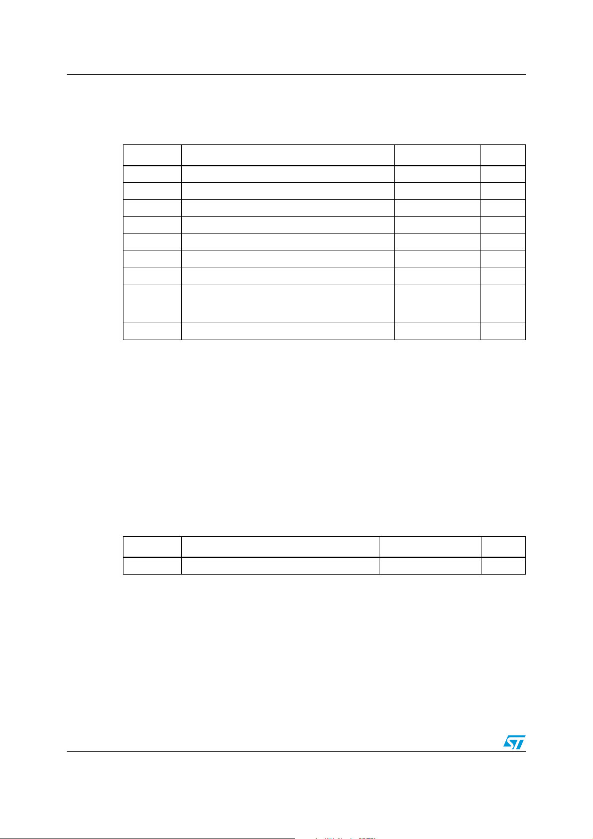
Table 1. Absolute maximum ratings
Symbol Parameter Value Unit
(1)
(4)
(2)
6V
(3)
Ω), done for all couples of pin
3.5
1.5
200
(5)
kV
kV
V
T
R
R
V
V
oper
T
T
CC
in
stg
j
thjc
thja
Supply voltage
Maximum input voltage swing 0 to 1.5 V
Operating free air temperature range -40 to +85 °C
Storage temperature -65 to +150 °C
Maximum junction temperature 150 °C
SO-8 thermal resistance junction to case 28 °C/W
SO-8 thermal resistance junction to ambient area 157 °C/W
HBM: human body model
ESD
CDM: charged device model
MM: machine model
Output short-circuit
1. All voltage values are with respect to network terminal.
2. Human body model: 100 pF discharged through a 1.5 kΩ resistor between two pins of the device, done for
all couples of pin combinations with other pins floating.
3. Charged device model: all pins plus package are charged together to the specified voltage and then
discharged directly to the ground.
4. Machine model: a 200 pF capacitor is charged to the specified voltage, then discharged directly between
two pins of the device with no external series resistor (internal resistor < 5
combinations with other pins floating.
5. An output current limitation protects the circuit from transient currents. Short-circuits can cause excessive
heating. Destructive dissipation can result from short-circuits on amplifiers.
2 Operating conditions
Table 2. Operating conditions
Symbol Parameter Value Unit
V
CC
1. This range is guaranteed by design (the product is tested in full production at a 5 V single power supply).
2/12 Doc ID 13895 Rev 2
Power supply voltage 4.5 to 5.5
(1)
V

TSH103 Electrical characteristics
3 Electrical characteristics
Table 3. VCC = +5 V single supply, T
= 25° C (unless otherwise specified)
amb
Symbol Parameter Test conditions Min. Typ. Max. Unit
DC performance
= 150 Ω 100 310 430
R
V
DC
I
ib
I
CC
Output DC shift
Input bias current
Supply current per channel
G DC voltage gain
V
V
I
OUT
OH
OL
High level output voltage RL = 150 Ω 3.9 V
Low level output voltage RL = 150 Ω 41 46 mV
I
sink/Isource
L
-40° C < T
= 0 V 1.2
V
in
-40° C < T
V
= 0.5 V DC 5.5 7.1
in
-40° C < T
= 150 Ω 1.93 1.97 2
R
L
-40° C < T
< +85° C 312
amb
< +85° C 1.4
amb
< +85° C 5.6
amb
< +85° C 1.96
amb
56 mA
Video performance
-3 dB bandwidth Small signal, RL = 150 Ω 9.4
F
Cut
F
att
-1 dB bandwidth Small signal, R
= 150 Ω 5.1 7.4
L
Filter attenuation Small signal, F= 27 MHz 37 dB
gd Group delay 0 to 5 MHz 10 ns
mV
μA
mA
V/V
MHz
dG Differential gain R
dPh Differential phase R
= 150 Ω 0.5 %
L
= 150 Ω 0.5 °
L
Noise
en Input voltage noise 100 kHz 76 nV/√Hz
Doc ID 13895 Rev 2 3/12

Electrical characteristics TSH103
Figure 1. Frequency response Figure 2. Gain flatness
10
5
0
-5
-10
-15
-20
-25
-30
Gain (dB)
-35
-40
-45
Vcc = +4.5V, +5V, +5.5V
-50
Small signal
-55
Load = 150
-60
100k 1M 10M 100M
Ω
27MHz
Frequency (Hz)
7.0
6.8
6.6
6.4
6.2
6.0
5.8
Gain (dB)
5.6
5.4
Vcc = +4.5V, +5V, +5.5V
Small signal
5.2
Load = 150
5.0
100k 1M 10M
Ω
Frequency (Hz)
Figure 3. Frequency response (large signal) Figure 4. Distortion
10
5
0
-5
-10
-15
-20
-25
-30
Gain (dB)
-35
-40
-45
Vcc = +4.5V, +5V, +5.5V
-50
Vout = 2Vp-p
-55
Load = 150
-60
100k 1M 10M 100M
Ω
Frequency (Hz)
-40
-45
-50
-55
-60
-65
-70
Distortion (dB)
-75
-80
-85
-90
0.0 0.5 1.0 1.5 2.0 2.5 3.0 3.5 4.0
H2
H3
Output Amplitude (Vp-p)
Figure 5. Quiescent current vs. supply Figure 6. Input noise vs. frequency
6.0
5.5
5.0
4.5
4.0
3.5
3.0
2.5
Icc (mA)
2.0
1.5
1.0
0.5
0.0
0.0 0.5 1.0 1.5 2.0 2.5 3.0 3.5 4.0 4.5 5.0 5.5
no input signal
no load
Vcc (V)
260
240
220
200
180
160
140
(nV/VHz)
120
n
e
100
80
60
40
1k 10k 100k 1M
No load
Input to GND
Vcc=+5V
Frequency (Hz)
Vcc = +5V
Vicm = +0.5V
F = 1MHz
Load = 150
Ω
4/12 Doc ID 13895 Rev 2
 Loading...