

Low cost high-side current sense amplifier
pOut
Features
■ Independent supply and input common-mode
voltages
■ Wide common-mode operating range: 2.8 V to
24 V
■ Wide supply voltage range: 4 to 24 V
■ Low current consumption: I
■ Internally fixed gain: 20 V/V, 50 V/V or 100 V/V
■ Buffered output
Applications
■ Desktop computers and servers SMPS
■ Photovoltaic/solar systems
■ Battery chargers
■ Notebook computers
■ DC motor control
max = 1 mA
CC
Gnd
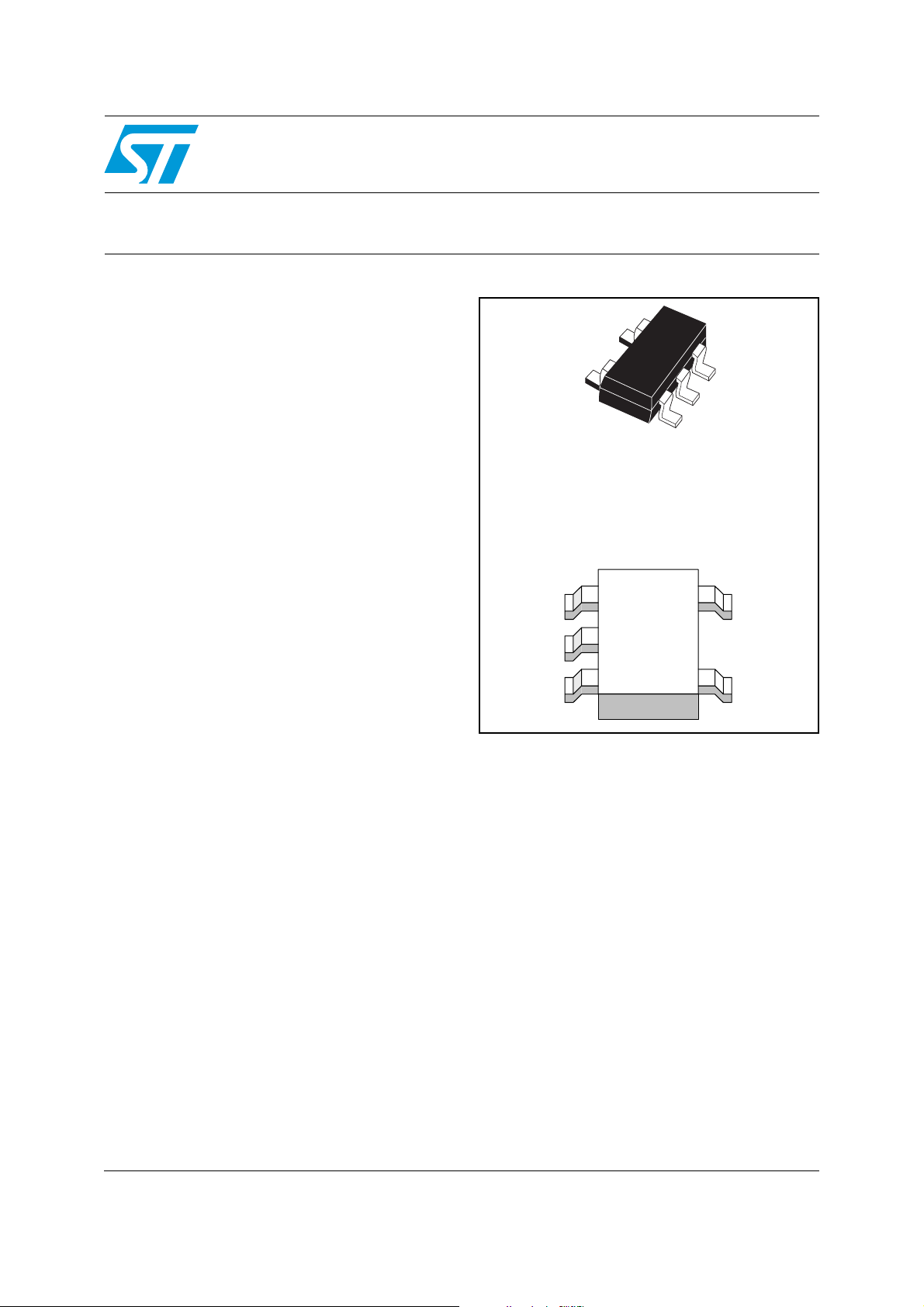
SOT23-5
(Plastic package)
Pin connections
(top view)
1
2
3V
TSC888
L
5
Vcc
4
Vm
Description
The TSC888 measures a small differential voltage
on a high-side shunt resistor and translates it into
a ground-referenced output voltage. The gain is
internally fixed.
Wide input common-mode voltage range, low
quiescent current, and tiny SOT23-5 packaging
make the TSC888 ideal for use in a wide variety
of applications.
Input common-mode and power supply voltages
are independent. Common-mode voltage can
range from 2.8 V to 24 V in operating conditions.
Current consumption lower than 1 mA and wide
supply voltage range allow to connect the power
supply to either side of the current measurement
shunt with minimal error.
June 2008 Rev 1 1/7
www.st.com
7
Application schematics and pin description TSC888
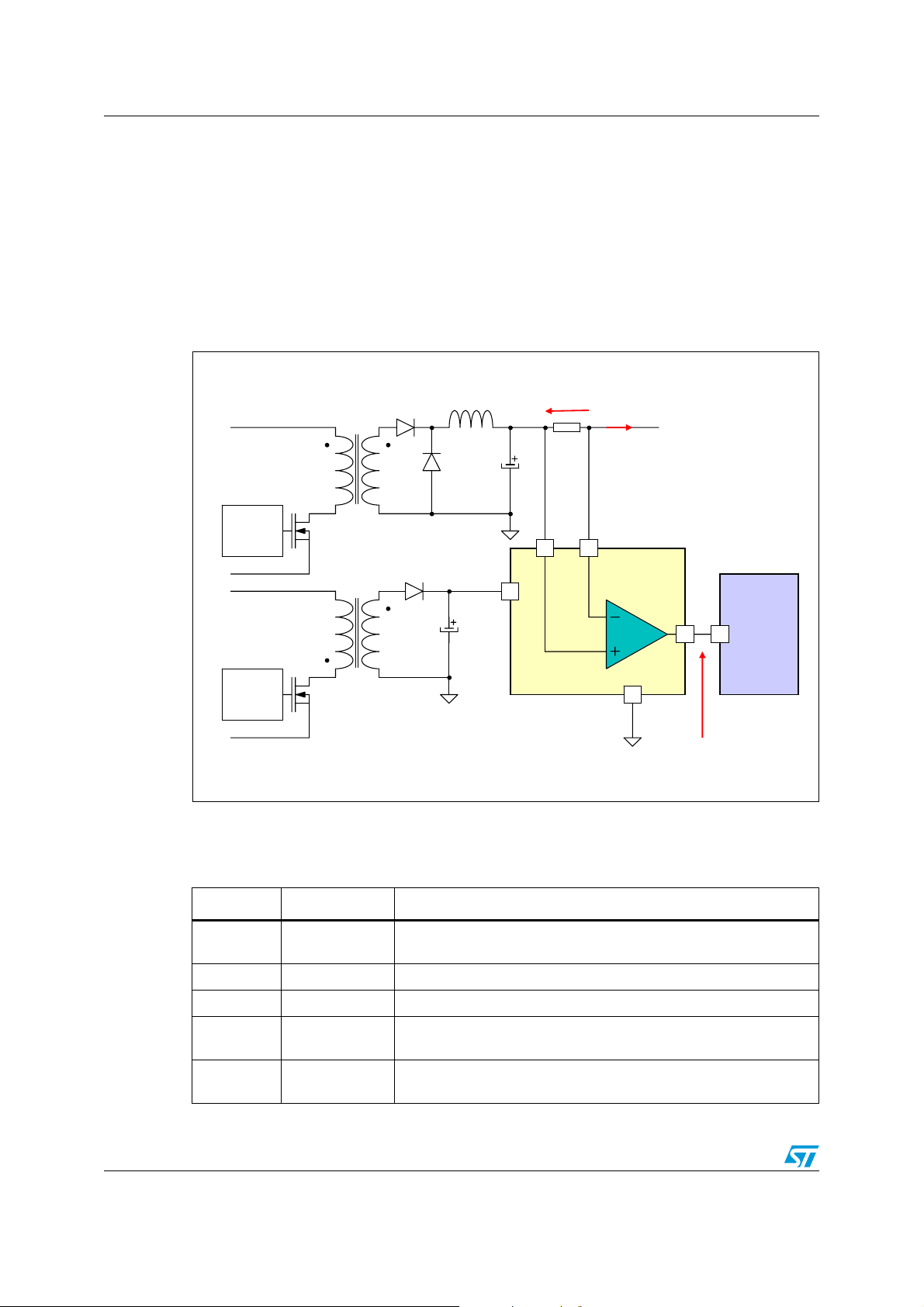
1 Application schematics and pin description
The TSC888 high-side current-sense amplifier features a 2.8 V to 24 V input common-mode
range that is independent of supply voltage. The main advantage of this feature is to allow
high-side current sensing at voltages much greater than the supply voltage (V
TSC888 can therefore be supplied by a 5 Vsb line and monitor a 3.3 V, 5 V or 12 V power
line. Considering the wide supply voltage operating range (4 V to 24 V) another option
available in most cases is to connect the V
pin to the Vp pin.
CC
Figure 1. Application schematics
V
sense
I
load
12V, 5V or 3.3V line
Main
PWM
controller
5Vsb
Vp
Vcc
Vm
TSC888
Out
). The
CC
Monitoring
device
Stand-by
PWM
controller
Gnd
V
out=Vsense.Av
Tab l e 1 describes the function of each pin. Their position is shown in the illustration on the
cover page and in Figure 1 above.
Table 1. Pin description
Symbol Type Function
Out Analog output
Gnd Power supply Ground line.
Vcc Power supply Positive power supply line.
Vp Analog input
Vm Analog input
The out voltage is proportional to the magnitude of the sense
voltage V
p-Vm
.
Connection for the external sense resistor. The measured current
enters the shunt on the V
side.
p
Connection for the external sense resistor. The measured current
exits the shunt on the V
side.
m
2/7
TSC888 Absolute maximum ratings and operating conditions
2 Absolute maximum ratings and operating conditions
Table 2. Absolute maximum ratings
Symbol Parameter Value Unit
V
id
V
in
V
CC
V
out
T
stg
T
R
thja
ESD
1. Voltage values are measured with respect to the Gnd pin.
2. Human body model: 100 pF discharged through a 1.5kΩ resistor between two pins of the device, done for
all couples of pin combinations with other pins floating.
3. Machine model: a 200 pF cap is charged to the specified voltage, then discharged directly between two
pins of the device with no external series resistor (internal resistor < 5 Ω), done for all couples of pin
combinations with other pins floating.
Table 3. Operating conditions
Input pins differential voltage (Vp-Vm)±2V
(1)
(1)
-0.3 to 30 V
-0.3 to 25 V
-0.3 to Vcc V
Input pin voltages (Vp, Vm)
DC supply voltage
(1)
DC output pin voltage
Storage temperature -55 to 150 °C
Maximum junction temperature 150 °C
j
SOT23-5 thermal resistance junction to ambient 250 °C/W
(3)
(2)
1kV
100 V
Human body model (HBM)
Machine model (MM)
Symbol Parameter Value Unit
V
T
V
CC
oper
icm
DC supply voltage from T
Operational temperature range (T
min
to T
max
min
to T
4.0 to 24 V
) -40 to 85 °C
max
Common mode operating range 2.8 to 24 V
3/7

Electrical characteristics TSC888
3 Electrical characteristics
The electrical characteristics given in the following tables are measured under the following
test conditions unless otherwise specified:
T
=25°C, Vcc=5V, V
Table 4. Supply
amb
sense=Vp-Vm
Symbol Parameter Test conditions Min. Typ. Max. Unit
=50mV, Vm=12V, no load on Out
I
Total supply current V
CC
= 0 1 mA
sense
Table 5. Input
Symbol Parameter Test conditions Min. Typ. Max. Unit
CMR
SVR
I
lk
I
ib
DC common mode rejection
Variation of V
versus V
out
icm
referred to input
Supply voltage rejection
Variation of V
versus V
out
cc
referred to input
Input leakage current Vcc=0V 1 µA
Input bias current V
2.8V< V
V
sense
4.0V< V
V
sense
sense
< 24V
icm
= 30mV
< 24V
CC
= 30mV
95 dB
95 dB
=0V 5.5 8 µA
Table 6. Output
Symbol Parameter Test conditions Min. Typ. Max. Unit
Av Gain
ΔV
I
sc
Total output voltage accuracy ±6 %
out
Short-circuit current
Output stage high-state saturation
V
OH
voltage
V
V
OL
Output stage low-state saturation
voltage
OH=VCC-Vout
TSC888A
TSC888B
TSC888C
OUT connected to V
GND
V
=1V
sense
=1mA
I
out
=-1V
V
sense
=1mA
I
out
CC
or
20
50
100
2mA
0.8 1 V
50 100 mV
V/V
4/7

TSC888 Package information
4 Package information
In order to meet environmental requirements, STMicroelectronics offers these devices in
ECOPACK
®
packages. These packages have a lead-free second level interconnect. The
category of second level interconnect is marked on the package and on the inner box label,
in compliance with JEDEC Standard JESD97. The maximum ratings related to soldering
conditions are also marked on the inner box label. ECOPACK is an STMicroelectronics
trademark. ECOPACK specifications are available at: www.st.com
.
Figure 2. SOT23-5 package mechanical drawing
Table 7. SOT23-5 package mechanical data
Dimensions
Ref.
Min. Typ. Max. Min. Typ. Max.
A0.901.4535.457.1
A1 0.00 0.15 0.00 5.9
A2 0.90 1.30 35.4 51.2
b0.350.5013.719.7
C 0.09 0.20 3.5 7.8
D 2.80 3.00 110.2 118.1
E 2.60 3.00 102.3 118.1
E1 1.50 1.75 59.0 68.8
e 0.95 37.4
e1 1.9 74.8
L0.350.5513.721.6
Millimeters Mils
5/7

Ordering information TSC888
5 Ordering information
Table 8. Order codes
Order code Temperature range Package Packaging Marking Gain
TSC888AILT
TSC888BILT O112 50
TSC888CILT O113 100
-40°C, +85°C SOT23-5 Tape & reel
O111 20
6 Revision history
Table 9. Document revision history
Date Revision Changes
26-Jun-2008 Rev 1 Initial release.
6/7

TSC888
Please Read Carefully:
Information in this document is provided solely in connection with ST products. STMicroelectronics NV and its subsidiaries (“ST”) reserve the
right to make changes, corrections, modifications or improvements, to this document, and the products and services described herein at any
time, without notice.
All ST products are sold pursuant to ST’s terms and conditions of sale.
Purchasers are solely responsible for the choice, selection and use of the ST products and services described herein, and ST assumes no
liability whatsoever relating to the choice, selection or use of the ST products and services described herein.
No license, express or implied, by estoppel or otherwise, to any intellectual property rights is granted under this document. If any part of this
document refers to any third party products or services it shall not be deemed a license grant by ST for the use of such third party products
or services, or any intellectual property contained therein or considered as a warranty covering the use in any manner whatsoever of such
third party products or services or any intellectual property contained therein.
UNLESS OTHERWISE SET FORTH IN ST’S TERMS AND CONDITIONS OF SALE ST DISCLAIMS ANY EXPRESS OR IMPLIED
WARRANTY WITH RESPECT TO THE USE AND/OR SALE OF ST PRODUCTS INCLUDING WITHOUT LIMITATION IMPLIED
WARRANTIES OF MERCHANTABILITY, FITNESS FOR A PARTICULAR PURPOSE (AND THEIR EQUIVALENTS UNDER THE LAWS
OF ANY JURISDICTION), OR INFRINGEMENT OF ANY PATENT, COPYRIGHT OR OTHER INTELLECTUAL PROPERTY RIGHT.
UNLESS EXPRESSLY APPROVED IN WRITING BY AN AUTHORIZED ST REPRESENTATIVE, ST PRODUCTS ARE NOT
RECOMMENDED, AUTHORIZED OR WARRANTED FOR USE IN MILITARY, AIR CRAFT, SPACE, LIFE SAVING, OR LIFE SUSTAINING
APPLICATIONS, NOR IN PRODUCTS OR SYSTEMS WHERE FAILURE OR MALFUNCTION MAY RESULT IN PERSONAL INJURY,
DEATH, OR SEVERE PROPERTY OR ENVIRONMENTAL DAMAGE. ST PRODUCTS WHICH ARE NOT SPECIFIED AS "AUTOMOTIVE
GRADE" MAY ONLY BE USED IN AUTOMOTIVE APPLICATIONS AT USER’S OWN RISK.
Resale of ST products with provisions different from the statements and/or technical features set forth in this document shall immediately void
any warranty granted by ST for the ST product or service described herein and shall not create or extend in any manner whatsoever, any
liability of ST.
ST and the ST logo are trademarks or registered trademarks of ST in various countries.
Information in this document supersedes and replaces all information previously supplied.
The ST logo is a registered trademark of STMicroelectronics. All other names are the property of their respective owners.
© 2008 STMicroelectronics - All rights reserved
STMicroelectronics group of companies
Australia - Belgium - Brazil - Canada - China - Czech Republic - Finland - France - Germany - Hong Kong - India - Israel - Italy - Japan -
Malaysia - Malta - Morocco - Singapore - Spain - Sweden - Switzerland - United Kingdom - United States of America
www.st.com
7/7
 Loading...