

Page 1
TS488
TS489
Pop-free 120 mW stereo headphone amplifier
Datasheet − production data
Features
■ Pop and click noise protection circuitry
■ Operating range from V
■ Standby mode active low (TS488) or high (TS489)
■ Output power:
– 120 mW at 5 V, into 16 Ω
with 0.1% THD+N max (1 kHz)
– 55 mW at 3.3 V, into 16 Ω
with 0.1% THD+N max (1 kHz)
■ Low current consumption: 2.7 mA max at 5 V
■ Ultra-low standby current consumption: 10 nA
typical
■ High signal-to-noise ratio
■ High crosstalk immunity: 102 dB (F = 1 kHz)
■ PSRR: 70 dB typ. (F = 1 kHz), inputs grounded
at 5 V
■ Unity-gain stable
■ Short-circuit protection circuitry
■ Available in lead-free MiniSO-8 & DFN8
2 mm x 2 mm
= 2.2 V to 5.5 V
CC
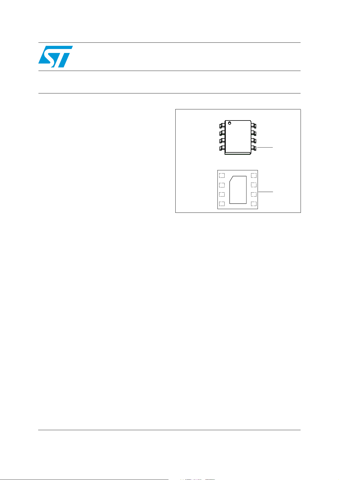
TS488IST - MiniSO-8
OUT (1 )
OUT (1 )
OUT (1 )
VIN (1)
VIN (1)
VIN (1)
BYPASS
BYPASS
BYPASS
GND
GND
GND
1
1
1
2
2
2
3
3
3
4
4
4
8
8
8
7
7
7
6
6
6
5
5
5
VCC
VCC
VCC
OUT (2 )
OUT (2 )
OUT (2 )
VIN (2)
VIN (2)
VIN (2)
SHUTDOWN
SHUTDOWN
SHUTDOWN
TS488IQT - DFN8
Vcc
Vcc
Vcc
OUT (1)
OUT (1)
OUT (1)
VIN (1)
VIN (1)
VIN (1)
Bypass
Bypass
Bypass
1
1
11
2
2
22
3
3
33
4
4
44
8
8
88
7
7
77
6
6
66
5
5
55
OUT
OUT
OUT
(2)
(2)
(2)
VIN (2)
VIN (2)
VIN (2)
Shutdown
Shutdown
Shutdown
GND
GND
GND
Applications
■ Headphone amplifiers
■ Mobile phones, PDAs, computer motherboards
■ High-end TVs, portable audio players
Description
The TS488/9 is an enhancement of TS486/7 that
eliminates pop and click noise and reduces the
number of external passive components.
The TS488/9 is a dual audio power amplifier
capable of driving, in single-ended mode, either a
16 Ω or a 32 Ω stereo headset.
Capable of descending to low voltages, it delivers
up to 31 mW per channel (into 16 Ω loads) of
continuous average power with 0.1% THD+N in
the audio bandwidth from a 2.5 V power supply.
An externally-controlled standby mode reduces
the supply current to 10 nA (typ.). The unity gain
stable TS488/9 is configured by external gainsetting resistors.
May 2012 Doc ID 11971 Rev 5 1/32
This is information on a product in full production.
www.st.com
32
Page 2

Contents TS488-TS489
Contents
1 Typical application schematic . . . . . . . . . . . . . . . . . . . . . . . . . . . . . . . . . 3
2 Absolute maximum ratings and operating conditions . . . . . . . . . . . . . 4
3 Electrical characteristics . . . . . . . . . . . . . . . . . . . . . . . . . . . . . . . . . . . . . 5
4 Application information . . . . . . . . . . . . . . . . . . . . . . . . . . . . . . . . . . . . . 22
4.1 Power dissipation and efficiency . . . . . . . . . . . . . . . . . . . . . . . . . . . . . . . 22
4.2 Total power dissipation . . . . . . . . . . . . . . . . . . . . . . . . . . . . . . . . . . . . . . . 23
4.3 Lower cutoff frequency . . . . . . . . . . . . . . . . . . . . . . . . . . . . . . . . . . . . . . . 23
4.4 Higher cutoff frequency . . . . . . . . . . . . . . . . . . . . . . . . . . . . . . . . . . . . . . 24
4.5 Gain setting . . . . . . . . . . . . . . . . . . . . . . . . . . . . . . . . . . . . . . . . . . . . . . . 25
4.6 Decoupling of the circuit . . . . . . . . . . . . . . . . . . . . . . . . . . . . . . . . . . . . . . 25
4.7 Standby mode . . . . . . . . . . . . . . . . . . . . . . . . . . . . . . . . . . . . . . . . . . . . . 25
4.8 Wake-up time . . . . . . . . . . . . . . . . . . . . . . . . . . . . . . . . . . . . . . . . . . . . . . 26
4.9 POP performance . . . . . . . . . . . . . . . . . . . . . . . . . . . . . . . . . . . . . . . . . . . 26
Connecting the headphones . . . . . . . . . . . . . . . . . . . . . . . . . . . . . . . . . . . . . . . . . 27
5 Package mechanical data . . . . . . . . . . . . . . . . . . . . . . . . . . . . . . . . . . . . 28
5.1 MiniSO-8 package . . . . . . . . . . . . . . . . . . . . . . . . . . . . . . . . . . . . . . . . . . 28
5.2 DFN8 package . . . . . . . . . . . . . . . . . . . . . . . . . . . . . . . . . . . . . . . . . . . . . 29
6 Ordering information . . . . . . . . . . . . . . . . . . . . . . . . . . . . . . . . . . . . . . . 30
7 Revision history . . . . . . . . . . . . . . . . . . . . . . . . . . . . . . . . . . . . . . . . . . . 31
2/32 Doc ID 11971 Rev 5
Page 3
TS488-TS489 Typical application schematic
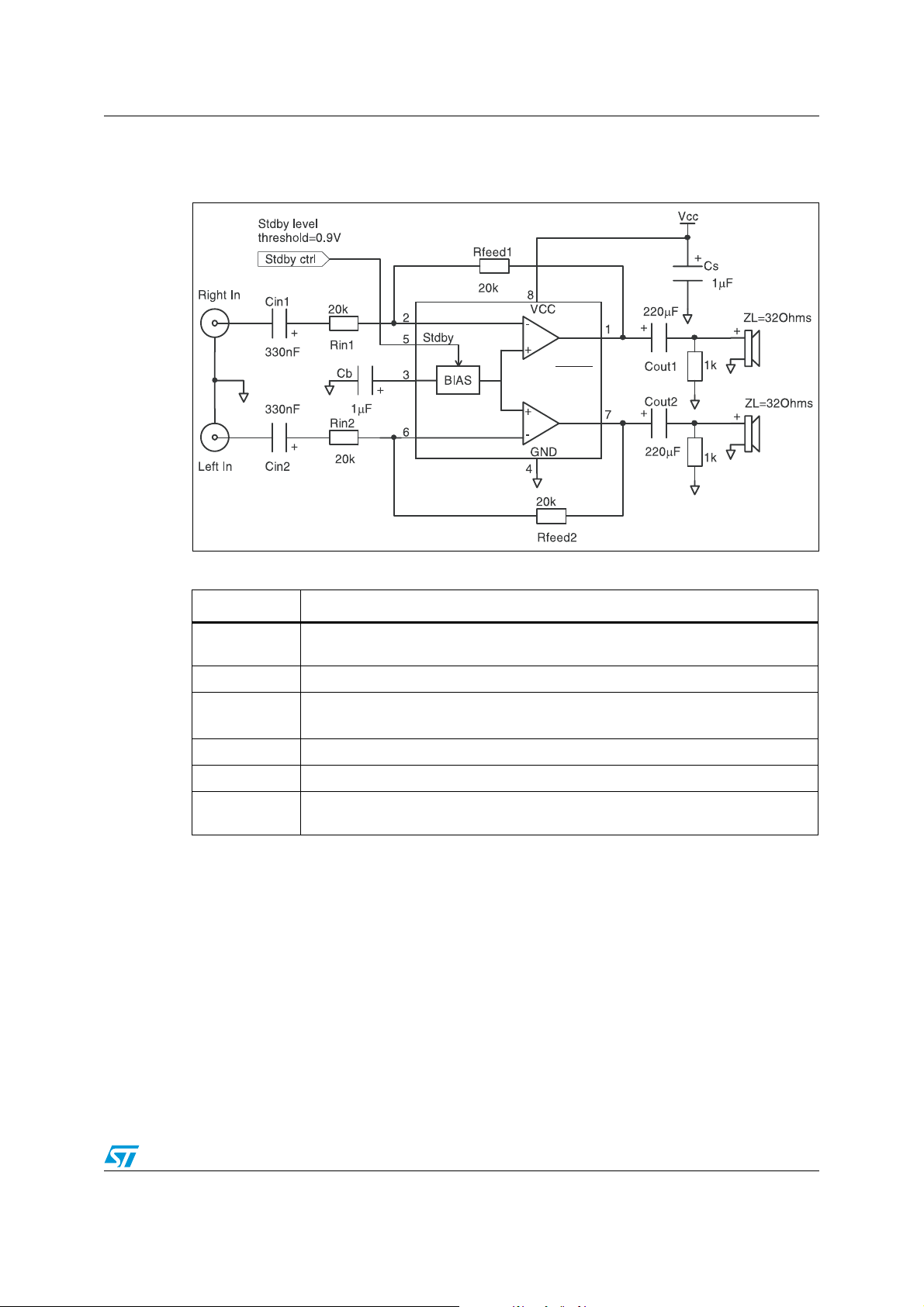
1 Typical application schematic
Figure 1. Typical application for the TS488-TS489
TS488=stdby
TS489=stdby
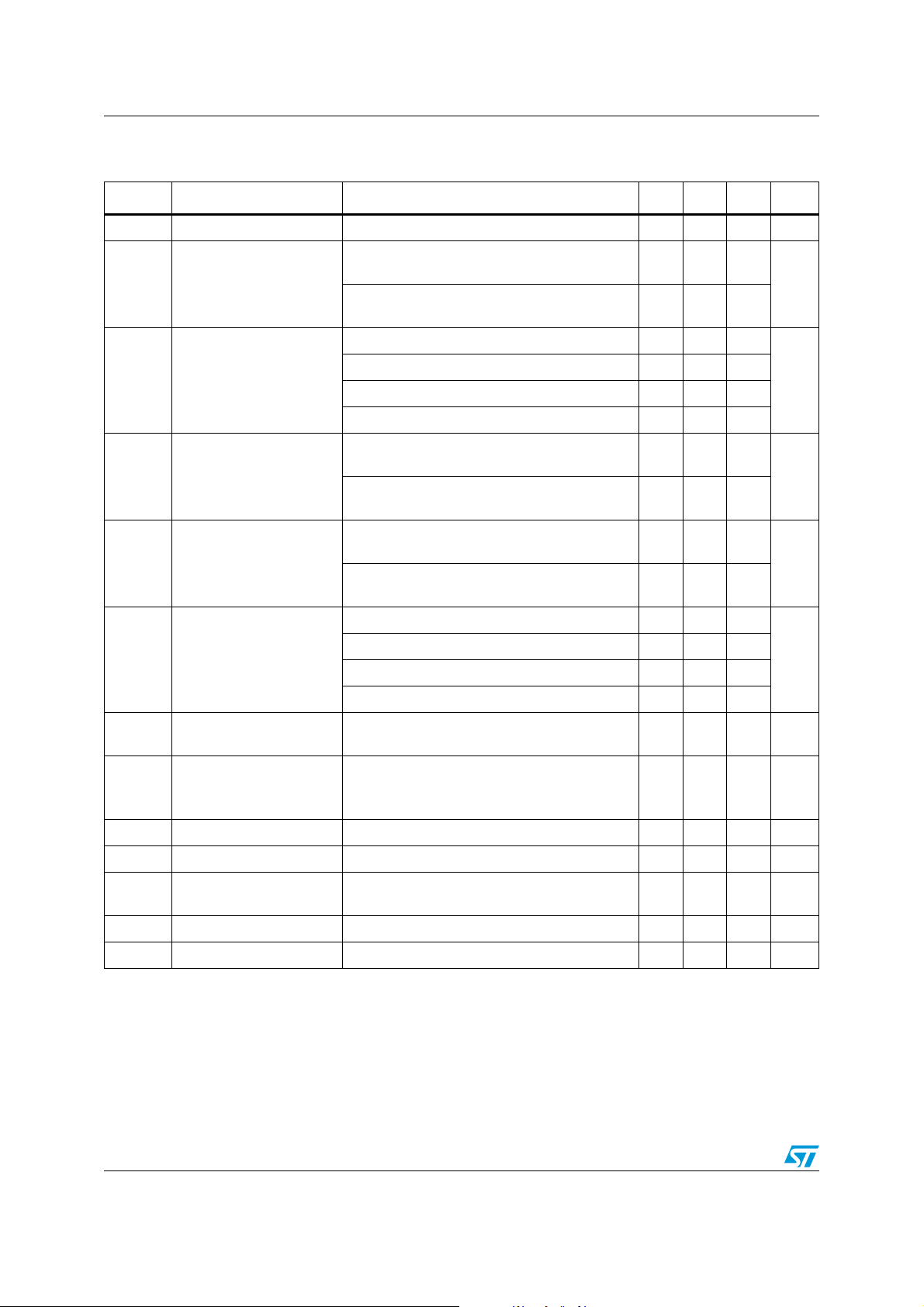
Table 1. Application component information
Component Functional description
R
C
R
feed1,2
C
out1,2
in1,2
in1,2
C
s
C
b
Inverting input resistor that sets the closed loop gain in conjunction with R
This resistor also forms a high pass filter with Cin (F
Input coupling capacitor that blocks the DC voltage at the amplifier’s input terminal.
Feedback resistor that sets the closed loop gain in conjunction with Rin.
AV= Closed Loop Gain= -R
feed/Rin
.
Supply output capacitor that provides power supply filtering.
Bypass capacitor that provides half supply filtering.
Output coupling capacitor that blocks the DC voltage at the load input terminal.
This capacitor also forms a high pass with R
(F
L
= 1 / (2 x Pi x R
c
= 1 / (2 x Pi x R
c
x C
L
x Cin)).
in
out
)).
feed
.
Doc ID 11971 Rev 5 3/32
Page 4
Absolute maximum ratings and operating conditions TS488-TS489
2 Absolute maximum ratings and operating conditions
Table 2. Absolute maximum ratings
Symbol Parameter Value Unit
V
CC
V
T
stg
T
Supply voltage
Input voltage -0.3 V to V
i
Storage temperature -65 to +150 °C
Maximum junction temperature 150 °C
j
Thermal resistance junction-to-ambient
R
thja
MiniSO-8
DFN8
Power dissipation
P
diss
MiniSO-8
DFN8
ESD Human body model (pin to pin) 2 kV
ESD
Machine model
220 pF - 240 pF (pin to pin)
(1)
(2)
6V
+0.3 V V
CC
215
°C/W
70
:
0.58
W
1.79
200 V
Latch-up Latch-up immunity (all pins) 200 mA
Lead temperature (soldering, 10 sec) 250 °C
Output short-circuit to V
1. All voltage values are measured with respect to the ground pin.
2. P
3. Attention must be paid to continuous power dissipation (VDD x 250 mA). Short-circuits can cause
Table 3. Operating conditions
is calculated with T
diss
excessive heating and destructive dissipation. Exposing the IC to a short-circuit for an extended period of
time will dramatically reduce the product’s life expectancy.
= 25 °C, Tj= 150 °C.
amb
or GND continuous
CC
(3)
Symbol Parameter Value Unit
V
T
CC
R
oper
Supply voltage 2.2 to 5.5 V
Load resistor ≥ 16 Ω
L
Operating free air temperature range -40 to + 85 °C
Load capacitor:
C
L
= 16 to 100 Ω
R
L
RL > 100 Ω
400
100
Standby voltage input:
V
STBY
TS488 active, TS489 in standby
TS488 in standby, TS489 active
1.5 ≤ V≤ V
GND ≤ V
STBY
CC
≤ 0.4
(1)
Thermal resistance junction-to-ambient
R
thja
1. The minimum current consumption (I
temperature range.
2. When mounted on a 4-layer PCB.
MiniSO-8
(2)
DFN8
190
40
) is guaranteed at GND (TS488) or VCC (TS489) for the whole
STBY
pF
V
°C/W
4/32 Doc ID 11971 Rev 5
Page 5
TS488-TS489 Electrical characteristics
3 Electrical characteristics
Table 4. Electrical characteristics at VCC=+5 V
with GND = 0 V, T
= 25 °C (unless otherwise specified)
amb
Symbol Parameter Conditions Min. Typ. Max. Unit
I
I
STBY
P
THD+N
PSRR
V
SNR Signal-to-noise ratio
Supply current No input signal, no load 2 2.7 mA
CC
No input signal, V
RL = 32 Ω
= GND for TS488,
STBY
10 1000
Standby current
Output power
out
Total harmonic distortion
+ noise
Power supply rejection
ratio, inputs grounded
Output swing
O
No input signal, V
STBY=VCC
RL = 32 Ω
THD+N = 0.1% max, F = 1 kHz, R
THD+N = 1% max, F = 1 kHz, R
THD+N = 0.1% max, F = 1 kHz, R
THD+N = 1% max, F = 1 kHz, R
=-1, RL=32 Ω, P
A
V
out
20 Hz ≤ F ≤ 20 kHz
A
=-1, RL=16 Ω, P
V
out
20 Hz ≤ F ≤ 20 kHz
AV=-1, RL ≥ 16 Ω, Cb=1 µF, F = 1 kHz,
= 200 mVpp
V
ripple
(1)
=-1, RL ≥ 16 Ω, Cb=1 µF, F = 217 Hz,
A
V
V
= 200 mVpp
ripple
: RL=32 Ω 0.23 0.31
V
OL
V
: RL= 32 Ω 4.53 4.72
OH
: RL=16 Ω 0.44 0.57
V
OL
V
: RL= 16 Ω 4.18 4.48
OH
A-weighted, A
=-1, RL=32 Ω,
V
THD+N < 0.4%, 20 Hz ≤ F ≤ 20 kHz
for TS489,
=60 mW,
=90 mW,
=32 Ω 75
L
=32 Ω 70 80
L
=16 Ω 120
L
=16 Ω 100 130
L
64 70
62 68
10 1000
0.3
0.3
105 dB
nA
mW
%
dB
V
Crosstalk Channel separation
Input capacitance 1 pF
C
i
GBP Gain bandwidth product R
SR
V
t
1. Guaranteed by design and evaluation.
Slew rate, unity gain
inverting
Input offset voltage V
IO
Wake-up time 100 ms
wu
R
= 32 Ω, AV=-1
L
F = 1 kHz
F = 20 Hz to 20 kHz
= 32 Ω 1.1 MHz
L
-102
-84
dB
RL= 16 Ω 0.65 V/μs
icm=VCC
/2 1 20 mV
Doc ID 11971 Rev 5 5/32
Page 6
Electrical characteristics TS488-TS489
Table 5. Electrical characteristics at VCC=+3.3 V
with GND = 0 V, T
= 25 °C (unless otherwise specified)
amb
(1)
Symbol Parameter Conditions Min. Typ. Max. Unit
I
I
STBY
P
THD+N
PSRR
V
SNR Signal-to-noise ratio
Supply current No input signal, no load 1.8 2.5 mA
CC
No input signal, V
RL = 32 Ω
= GND for TS488,
STBY
10 1000
Standby current
Output power
out
Total harmonic distortion
+ noise
Power supply rejection
ratio, inputs grounded
Output swing
O
No input signal, V
STBY=VCC
RL = 32 Ω
THD+N = 0.1% max, F = 1 kHz, R
THD+N = 1% max, F = 1 kHz, R
THD+N = 0.1% max, F = 1 kHz, R
THD+N = 1% max, F = 1 kHz, R
=-1, RL=32 Ω, P
A
V
out
20 Hz ≤ F ≤ 20 kHz
=-1, RL=16 Ω, P
A
V
out
20 Hz ≤ F ≤ 20 kHz
AV=-1, RL ≥ 16 Ω, Cb=1 µF, F = 1 kHz,
= 200 mVpp
V
ripple
(2)
=-1, RL ≥ 16 Ω, Cb=1 µF, F = 217 Hz,
A
V
V
= 200 mVpp
ripple
: RL=32 Ω 0.15 0.2
V
OL
V
: RL=32 Ω 3.03 3.12
OH
: RL=16 Ω 0.28 0.36
V
OL
V
: RL=16 Ω 2.82 2.97
OH
A-weighted, A
=-1, RL=32 Ω,
V
THD+N < 0.4%, 20 Hz ≤F ≤ 20 kHz
for TS489,
= 16 mW,
= 35 mW,
=32 Ω 34
L
=32 Ω 30 35
L
=16 Ω 55
L
=16 Ω 47 57
L
63 69
61 67
10 1000
0.3
0.3
102 dB
nA
mW
%
dB
V
R
=32 Ω, AV=-1
Crosstalk Channel separation
L
F = 1 kHz
F = 20 Hz to 20 kHz
Input capacitance 1 pF
C
i
GBP Gain bandwidth product R
SR
V
t
1. All electrical values are guaranteed with correlation measurements at 2.5 V and 5 V.
2. Guaranteed by design and evaluation.
Slew rate, unity gain
inverting
Input offset voltage V
IO
Wake-up time 100 ms
wu
=32 Ω 1.1 MHz
L
RL=16 Ω 0.6 V/μs
icm=VCC
/2 1 20 mV
6/32 Doc ID 11971 Rev 5
-102
-84
dB
Page 7

TS488-TS489 Electrical characteristics
Table 6. Electrical characteristics at VCC=+2.5 V
with GND = 0 V, T
Symbol Parameter Conditions Min. Typ. Max. Unit
= 25 °C (unless otherwise specified)
amb
I
I
STBY
P
THD+N
PSRR
V
Supply current No input signal, no load 1.8 2.5 mA
CC
Standby current
Output power
out
Total harmonic distortion
+ noise
Power supply rejection
ratio, inputs grounded
Output swing
O
SNR Signal-to-noise ratio
Crosstalk Channel separation
No input signal, V
= GND for TS488,
STBY
RL = 32 Ω
No input signal, V
= 32 Ω
R
L
STBY=VCC
THD+N = 0.1% max, F = 1 kHz, R
THD+N = 1% max, F = 1 kHz, R
THD+N = 0.1% max, F = 1 kHz, R
THD+N = 1% max, F = 1 kHz, R
A
= -1, RL=32 Ω, P
V
= 10 mW,
out
20 Hz ≤ F ≤ 20 kHz
=-1, RL=16 Ω, P
A
V
= 16 mW,
out
20 Hz ≤ F ≤ 20 kHz
AV = -1, RL ≥ 16 Ω, Cb=1 µF, F = 1 kHz,
V
= 200 mVpp
ripple
(1)
A
= -1, RL ≥ 16 Ω, Cb=1 µF, F = 217 Hz,
V
V
= 200 mVpp
ripple
: RL=32 Ω 0.12 0.16
V
OL
V
: RL=32 Ω 2.3 2.36
OH
: RL=16 Ω 0.22 0.28
V
OL
: RL=16 Ω 2.15 2.25
V
OH
A-weighted, A
= -1, RL=32 Ω,
V
THD+N < 0.4%, 20 Hz ≤ F ≤ 20 kHz
=32 Ω, AV = -1
R
L
F = 1 kHz
F = 20 Hz to 20 kHz
for TS489,
=32 Ω 19
L
=32 Ω 18 20
L
=16 Ω 31
L
=16 Ω 27 32
L
10 1000
10 1000
mW
0.3
0.3
68
66
100 dB
-102
-84
nA
%
dB
V
dB
Input capacitance 1 pF
C
i
GBP Gain bandwidth product R
SR
V
t
1. Guaranteed by design and evaluation.
Slew rate, unity gain
inverting
Input offset voltage V
IO
Wake-up time 100 ms
wu
=32 Ω 1.1 MHz
L
=16 Ω 0.6 V/μs
R
L
= VCC/2 1 20 mV
icm
Doc ID 11971 Rev 5 7/32
Page 8
Electrical characteristics TS488-TS489
Table 7. Index of graphics
Description Figure
Open-loop frequency response Figure 2 to Figure 11
Power derating curves Figure 12 to Figure 13
Signal-to-noise ratio vs. power supply voltage Figure 14 to Figure 19
Power dissipation vs. output power per channel Figure 20 to Figure 22
Power supply rejection ratio vs. frequency Figure 23 to Figure 25
Total harmonic distortion plus noise vs. output power Figure 26 to Figure 43
Total harmonic distortion plus noise vs. frequency Figure 44 to Figure 52
Output power vs. load resistance Figure 53 to Figure 55
Output power vs. power supply voltage Figure 56, Figure 57
Output voltage swing vs. power supply voltage Figure 58
Current consumption vs. power supply voltage Figure 59
Current consumption vs. standby voltage Figure 60 to Figure 65
Crosstalk vs. frequency Figure 66 to Figure 77
8/32 Doc ID 11971 Rev 5
Page 9
TS488-TS489 Electrical characteristics
Figure 2. Open-loop frequency response Figure 3. Open-loop frequency response
Gain (dB)
125
100
-25
-50
-75
Ω
=25°C
225
180
135
90
45
0
Vcc=2.5V
RL=16
gain
T
75
AMB
50
25
0
phase
-45
-90
0
10
2
10
4
10
6
10
-135
8
10
Frequency (Hz)
125
100
75
gain
Vcc=5V
RL=16
T
AMB
50
25
Gain (dB)
Phase (°)
0
phase
-25
-50
-75
0
10
2
10
4
10
6
10
Ω
=25°C
225
180
135
90
45
0
-45
-90
-135
8
10
Frequency (Hz)
Figure 4. Open-loop frequency response Figure 5. Open-loop frequency response
125
100
75
gain
Vcc=2.5V
RL=16
CL=400pF
T
AMB
50
25
Gain (dB)
0
phase
-25
-50
-75
0
10
2
10
4
10
6
10
Ω
=25°C
225
180
135
90
45
0
-45
-90
-135
8
10
Frequency (Hz)
125
100
75
gain
Vcc=5V
RL=16
CL=400pF
T
AMB
50
25
Gain (dB)
Phase (°)
0
phase
-25
-50
-75
0
10
2
10
4
10
6
10
Ω
=25°C
225
180
135
90
45
0
-45
-90
-135
8
10
Frequency (Hz)
Phase (°)
Phase (°)
Figure 6. Open-loop frequency response Figure 7. Open-loop frequency response
125
100
75
gain
Vcc=2.5V
RL=32
T
AMB
50
25
Gain (dB)
0
phase
-25
-50
-75
0
10
2
10
4
10
6
10
Ω
=25°C
225
180
135
90
45
0
-45
-90
-135
8
10
Frequency (Hz)
Doc ID 11971 Rev 5 9/32
125
100
75
gain
Vcc=5V
RL=32
T
AMB
50
25
Gain (dB)
Phase (°)
0
phase
-25
-50
-75
0
10
2
10
4
10
6
10
Ω
=25°C
225
180
135
90
45
0
-45
-90
-135
8
10
Frequency (Hz)
Phase (°)
Page 10

Electrical characteristics TS488-TS489
Figure 8. Open-loop frequency response Figure 9. Open-loop frequency response
125
100
75
gain
Vcc=2.5V
RL=32
CL=400pF
T
AMB
50
25
Gain (dB)
0
phase
-25
-50
-75
0
10
2
10
4
10
Frequency (Hz)
6
10
Ω
=25°C
225
180
135
90
45
0
-45
-90
-135
8
10
125
100
75
gain
Vcc=5V
RL=32
CL=400pF
T
AMB
50
25
Gain (dB)
Phase (°)
0
phase
-25
-50
-75
0
10
2
10
4
10
Frequency (Hz)
6
10
Ω
=25°C
225
180
135
90
45
0
-45
-90
-135
8
10
Figure 10. Open-loop frequency response Figure 11. Open-loop frequency response
125
100
75
gain
Vcc=2.5V
RL=600
T
AMB
50
25
Gain (dB)
0
phase
-25
-50
-75
0
10
2
10
4
10
Frequency (Hz)
6
10
Ω
=25°C
225
180
135
90
45
0
-45
-90
-135
8
10
125
100
75
gain
Vcc=5V
RL=600
T
AMB
50
25
Gain (dB)
Phase (°)
0
phase
-25
-50
-75
0
10
2
10
4
10
Frequency (Hz)
6
10
=25°C
225
180
Ω
135
90
45
0
-45
-90
-135
8
10
Phase (°)
Phase (°)
Figure 12. Power derating curves Figure 13. Power derating curves
0.8
0.6
4-layer PCB
0.4
0.2
No Heat sink
Package Power Dissipation (W)
0.0
0 25 50 75 100 125 150
Ambiant Temperature (°C)
10/32 Doc ID 11971 Rev 5
MiniSO8
3
4-layer PCB
2
1
Package Power Dissipation (W)
0
0 25 50 75 100 125 150
Ambiant Temperature (°C)
DFN8
No heatsink
Page 11

TS488-TS489 Electrical characteristics
Figure 14. Signal-to-noise ratio vs. power
supply voltage
110
A-weighted Filter
Av=-1, T
108
Cb=1μF
THD+N<0.4%
106
104
102
Signal to Noise Ratio (dB)
100
98
23456
=25°C
AMB
Power Supply Voltage (V)
RL=32
RL=16
Ω
Figure 16. Signal-to-noise ratio vs. power
supply voltage
106
A-weighted Filter
104
102
Av=-2, T
Cb=1μF
THD+N<0.4%
AMB
=25°C
Figure 15. Signal-to-noise ratio vs. power
supply voltage
106
Unweighted Filter
(20Hz-20kHz)
104
Av=-1, T
Cb=1μF
102
THD+N<0.4%
100
98
Ω
Signal to Noise Ratio (dB)
96
94
23456
=25°C
AMB
RL=32
Power Supply Voltage (V)
RL=16
Ω
Ω
Figure 17. Signal-to-noise ratio vs. power
supply voltage
102
Unweighted Filter
(20Hz-20kHz)
100
Av=-2, T
Cb=1μF
98
THD+N<0.4%
AMB
=25°C
100
98
Signal to Noise Ratio (dB)
96
94
23456
Power Supply Voltage (V)
RL=32
RL=16
Ω
Ω
Figure 18. Signal-to-noise ratio vs. power
supply voltage
100
A-weighted Filter
Av=-4, T
98
Cb=1μF
THD+N<0.4%
96
94
92
Signal to Noise Ratio (dB)
90
88
23456
=25°C
AMB
RL=32
Power Supply Voltage (V)
RL=16
Ω
Ω
RL=16
96
94
Signal to Noise Ratio (dB)
92
90
23456
Power Supply Voltage (V)
RL=32
Ω
Ω
Figure 19. Signal-to-noise ratio vs. power
supply voltage
98
Unweighted Filter
(20Hz-20kHz)
96
Av=-4, T
Cb=1μF
94
THD+N<0.4%
92
90
Signal to Noise Ratio (dB)
88
86
23456
=25°C
AMB
RL=32
Power Supply Voltage (V)
RL=16
Ω
Ω
Doc ID 11971 Rev 5 11/32
Page 12

Electrical characteristics TS488-TS489
Figure 20. Power dissipation vs. output power
per channel
30
Vcc=2.5V, F=1kHz, THD+N<1%
25
20
15
10
Power Dissipation (mW)
5
0
0 5 10 15 20 25 30 35 40
RL=32Ω
Output Power (mW)
RL=16Ω
Figure 22. Power dissipation vs. output power
per channel
100
Vcc=5V, F=1kHz, THD+N<1%
80
60
RL=32Ω
40
Power Dissipation (mW)
20
0
0 20 40 60 80 100 120 140 160
Output Power (mW)
RL=16Ω
Figure 24. Power supply rejection ratio vs.
frequency
0
Inputs grounded, Vcc=3.3V,
-10
-20
-30
-40
PSRR (dB)
-50
-60
-70
-80
20
RL=16Ω, Cb=1μF, T
100 1k 10k
=25°C
AMB
Av=-2
Av=-1
Frequency (Hz)
Av=-4
20k
Figure 21. Power dissipation vs. output power
per channel
40
Vcc=3.3V, F=1kHz, THD+N<1%
35
30
25
20
15
10
Power Dissipation (mW)
5
0
0 10203040506070
RL=16Ω
RL=32Ω
Output Power (mW)
Figure 23. Power supply rejection ratio vs.
frequency
0
Inputs grounded, Av=-1,
-10
RL=16Ω, Cb=1μF, T
-20
-30
-40
PSRR (dB)
-50
-60
-70
-80
20
100 1k 10k
=25°C
AMB
Vcc=3.3V
Vcc=5V
Frequency (Hz)
Vcc=2.5V
20k
Figure 25. Power supply rejection ratio vs.
frequency
0
Inputs grounded, Av=-1,
-10
RL=16Ω, Vcc=3.3V, T
-20
-30
-40
PSRR (dB)
-50
-60
-70
-80
20
Cb=1μF
Cb=470nF
100 1k 10k
=25°C
AMB
Cb=220nF
Cb=100nF
Frequency (Hz)
20k
12/32 Doc ID 11971 Rev 5
Page 13

TS488-TS489 Electrical characteristics
Figure 26. Total harmonic distortion plus
noise vs. output power
10
F=1kHz, RL=16
AV=-1, T
BW=20Hz-120kHz
1
0.1
THD+N (%)
0.01
1E-3
1 10 100
Ω
=25°C
AMB
VCC=2.5V
Output Power (mW)
VCC=5V
VCC=3.3V
Figure 28. Total harmonic distortion plus
noise vs. output power
10
F=1kHz, RL=32
AV=-1, T
BW=20Hz-120kHz
1
AMB
Ω
=25°C
VCC=5V
Figure 27. Total harmonic distortion plus
noise vs. output power
10
200
F=20kHz, RL=16
AV=-1, T
BW=20Hz-120kHz
1
THD+N (%)
0.1
0.01
1 10 100
Ω
=25°C
AMB
VCC=2.5V
Output Power (mW)
VCC=5V
VCC=3.3V
Figure 29. Total harmonic distortion plus
noise vs. output power
10
F=20kHz, RL=32
AV=-1, T
BW=20Hz-120kHz
1
AMB
Ω
=25°C
VCC=5V
200
0.1
THD+N (%)
0.01
1E-3
1 10 100
VCC=3.3V
VCC=2.5V
Output Power (mW)
Figure 30. Total harmonic distortion plus
noise vs. output power
10
F=1kHz, RL=600
AV=-1, T
BW=20Hz-120kHz
1
0.1
THD+N (%)
0.01
1E-3
0.01 0.1 1
Ω
=25°C
AMB
Output Voltage (V
VCC=5V
VCC=3.3V
VCC=2.5V
RMS
)
VCC=3.3V
200
THD+N (%)
0.1
0.01
1 10 100
VCC=2.5V
Output Power (mW)
Figure 31. Total harmonic distortion plus
noise vs. output power
10
F=20kHz, RL=600
AV=-1, T
BW=20Hz-120kHz
1
0.1
THD+N (%)
0.01
3
1E-3
0.01 0.1 1
=25°C
AMB
Output Voltage (V
Ω
VCC=5V
VCC=3.3V
VCC=2.5V
RMS
200
3
)
Doc ID 11971 Rev 5 13/32
Page 14

Electrical characteristics TS488-TS489
Figure 32. Total harmonic distortion plus
noise vs. output power
10
F=1kHz, RL=16
AV=-2, T
BW=20Hz-120kHz
1
0.1
THD+N (%)
0.01
1E-3
1 10 100
Ω
=25°C
AMB
VCC=2.5V
Output Power (mW)
VCC=5V
VCC=3.3V
Figure 34. Total harmonic distortion plus
noise vs. output power
10
F=1kHz, RL=32
AV=-2, T
BW=20Hz-120kHz
1
AMB
Ω
=25°C
VCC=5V
Figure 33. Total harmonic distortion plus
noise vs. output power
10
200
F=20kHz, RL=16
AV=-2, T
BW=20Hz-120kHz
1
THD+N (%)
0.1
0.01
1 10 100
Ω
=25°C
AMB
VCC=2.5V
Output Power (mW)
VCC=5V
VCC=3.3V
Figure 35. Total harmonic distortion plus
noise vs. output power
10
F=20kHz, RL=32
AV=-2, T
BW=20Hz-120kHz
1
AMB
Ω
=25°C
VCC=5V
200
0.1
THD+N (%)
0.01
1E-3
1 10 100
VCC=3.3V
VCC=2.5V
Output Power (mW)
Figure 36. Total harmonic distortion plus
noise vs. output power
10
F=1kHz, RL=600
AV=-2, T
BW=20Hz-120kHz
1
0.1
THD+N (%)
0.01
1E-3
0.01 0.1 1
Ω
=25°C
AMB
Output Voltage (V
VCC=5V
VCC=3.3V
VCC=2.5V
RMS
)
VCC=3.3V
200
THD+N (%)
0.1
0.01
1 10 100
VCC=2.5V
Output Power (mW)
Figure 37. Total harmonic distortion plus
noise vs. output power
10
F=20kHz, RL=600
AV=-2, T
BW=20Hz-120kHz
1
THD+N (%)
0.1
3
0.01
0.01 0.1 1
AMB
=25°C
Ω
VCC=5V
VCC=3.3V
VCC=2.5V
Output Voltage (V
RMS
)
200
3
14/32 Doc ID 11971 Rev 5
Page 15

TS488-TS489 Electrical characteristics
Figure 38. Total harmonic distortion plus
noise vs. output power
10
F=1kHz, RL=16
AV=-4, T
BW=20Hz-120kHz
1
0.1
THD+N (%)
0.01
1E-3
1 10 100
Ω
=25°C
AMB
Output Power (mW)
VCC=5V
VCC=3.3V
VCC=2.5V
Figure 40. Total harmonic distortion plus
noise vs. output power
10
F=1kHz, RL=32
AV=-4, T
BW=20Hz-120kHz
1
0.1
THD+N (%)
0.01
AMB
Ω
=25°C
VCC=3.3V
VCC=2.5V
VCC=5V
Figure 39. Total harmonic distortion plus
noise vs. output power
10
200
F=20kHz, RL=16
AV=-4, T
BW=20Hz-120kHz
1
THD+N (%)
0.1
1 10 100
Ω
=25°C
AMB
VCC=2.5V
Output Power (mW)
VCC=5V
VCC=3.3V
Figure 41. Total harmonic distortion plus
noise vs. output power
10
F=20kHz, RL=32
AV=-4, T
BW=20Hz-120kHz
1
THD+N (%)
0.1
AMB
Ω
=25°C
VCC=3.3V
VCC=2.5V
VCC=5V
200
1E-3
1 10 100
Output Power (mW)
Figure 42. Total harmonic distortion plus
noise vs. output power
10
F=1kHz, RL=600
AV=-4, T
BW=20Hz-120kHz
1
0.1
THD+N (%)
0.01
1E-3
0.01 0.1 1
Ω
=25°C
AMB
Output Voltage (V
VCC=5V
VCC=3.3V
VCC=2.5V
RMS
)
200
0.01
1 10 100
Output Power (mW)
Figure 43. Total harmonic distortion plus
noise vs. output power
10
F=20kHz, RL=600
AV=-4, T
BW=20Hz-120kHz
1
THD+N (%)
0.1
3
0.01
0.01 0.1 1
AMB
=25°C
Ω
VCC=5V
VCC=3.3V
VCC=2.5V
Output Voltage (V
RMS
)
200
3
Doc ID 11971 Rev 5 15/32
Page 16

Electrical characteristics TS488-TS489
Figure 44. Total harmonic distortion plus
noise vs. frequency
1
RL=16
Ω,
AV=-1
BW=20Hz-120kHz
T
=25°C
AMB
0.1
Vcc=2.5V, Po=20mW
Vcc=3.3V, Po=40mW
THD+N (%)
Vcc=5V, Po=100mW
0.01
1E-3
20
100 1k 10k
Frequency (Hz)
Figure 46. Total harmonic distortion plus
noise vs. frequency
1
RL=600
Ω,
AV=-1
BW=20Hz-120kHz
T
=25°C
AMB
0.1
THD+N (%)
0.01
Vcc=2.5V, Vo=0.7V
Vcc=3.3V, Vo=1V
Vcc=5V, Po=1.6V
RMS
RMS
RMS
Figure 45. Total harmonic distortion plus
noise vs. frequency
1
RL=32
Ω,
AV=-1
BW=20Hz-120kHz
T
=25°C
AMB
0.1
Vcc=2.5V, Po=12mW
Vcc=3.3V, Po=25mW
THD+N (%)
Vcc=5V, Po=60mW
0.01
20k
1E-3
20
100 1k 10k
Frequency (Hz)
Figure 47. Total harmonic distortion plus
noise vs. frequency
1
RL=16
Ω,
AV=-2
BW=20Hz-120kHz
T
=25°C
AMB
0.1
THD+N (%)
0.01
Vcc=2.5V, Po=20mW
Vcc=3.3V, Po=40mW
Vcc=5V, Po=100mW
20k
1E-3
20
100 1k 10k
Frequency (Hz)
Figure 48. Total harmonic distortion plus
noise vs. frequency
1
RL=32
Ω,
AV=-2
BW=20Hz-120kHz
T
=25°C
AMB
THD+N (%)
0.1
0.01
1E-3
20
Vcc=2.5V, Po=12mW
Vcc=3.3V, Po=25mW
Vcc=5V, Po=60mW
100 1k 10k
Frequency (Hz)
20k
1E-3
20
100 1k 10k
Frequency (Hz)
Figure 49. Total harmonic distortion plus
noise vs. frequency
1
RL=600
Ω,
AV=-2
BW=20Hz-120kHz
T
=25°C
AMB
20k
THD+N (%)
0.1
0.01
1E-3
20
Vcc=2.5V, Vo=0.7V
Vcc=3.3V, Vo=1V
Vcc=5V, Po=1.6V
RMS
RMS
RMS
100 1k 10k
Frequency (Hz)
20k
20k
16/32 Doc ID 11971 Rev 5
Page 17

TS488-TS489 Electrical characteristics
Figure 50. Total harmonic distortion plus
noise vs. frequency
1
RL=16
Ω,
AV=-4
BW=20Hz-120kHz
T
=25°C
AMB
0.1
Vcc=2.5V, Po=20mW
Vcc=3.3V, Po=40mW
THD+N (%)
0.01
Vcc=5V, Po=100mW
1E-3
20
100 1k 10k
Frequency (Hz)
Figure 52. Total harmonic distortion plus
noise vs. frequency
1
RL=600
Ω,
AV=-4
BW=20Hz-120kHz
T
=25°C
AMB
0.1
THD+N (%)
0.01
Vcc=2.5V, Vo=0.7V
Vcc=3.3V, Vo=1V
RMS
RMS
Figure 51. Total harmonic distortion plus
noise vs. frequency
1
RL=32
Ω,
AV=-4
BW=20Hz-120kHz
T
=25°C
AMB
0.1
Vcc=2.5V, Po=12mW
Vcc=3.3V, Po=25mW
THD+N (%)
0.01
Vcc=5V, Po=60mW
20k
1E-3
20
100 1k 10k
Frequency (Hz)
Figure 53. Output power vs. load resistance
75
50
25
Output Power (mW)
THD+N=10%
Vcc=2.5V, F=1kHz
T
AMB
BW=20Hz-120kHz
THD+N=1%
=25°C
20k
1E-3
Vcc=5V, Po=1.6V
20
100 1k 10k
Frequency (Hz)
RMS
20k
0
8 16243240485664
Load Resistance (Ω)
Figure 54. Output power vs. load resistance Figure 55. Output power vs. load resistance
125
Vcc=3.3V, F=1kHz
T
=25°C
100
THD+N=10%
AMB
BW=20Hz-120kHz
75
THD+N=1%
50
Output Power (mW)
25
0
8 16243240485664
Load Resistance (Ω)
250
Vcc=5V, F=1kHz
T
=25°C
200
THD+N=10%
AMB
BW=20Hz-120kHz
150
THD+N=1%
100
Output Power (mW)
50
0
8 16243240485664
Load Resistance (Ω)
Doc ID 11971 Rev 5 17/32
Page 18

Electrical characteristics TS488-TS489
Figure 56. Output power vs. power supply
voltage
240
RL=16Ω, F=1kHz
T
AMB
=25°C
200
BW=20Hz-120kHz
160
120
80
Output Power (mW)
40
0
23456
Power Supply Voltage (V)
THD+N=10%
THD+N=1%
Figure 58. Output voltage swing vs. power
supply voltage
6
T
=25°C
AMB
5
4
(V)
OL
3
& V
OH
V
2
RL=16
Ω
1
RL=32
Ω
Figure 57. Output power vs. power supply
voltage
140
RL=32Ω, F=1kHz
120
T
=25°C
AMB
BW=20Hz-120kHz
100
80
60
THD+N=10%
Output Power (mW)
40
20
0
23456
Power Supply Voltage (V)
THD+N=1%
Figure 59. Current consumption vs. power
supply voltage
3
No Loads
2
1
Current Consumption (mA)
T
AMB
= 85°C
T
T
AMB
AMB
= 25°C
= -40°C
0
23456
Power Supply Voltage (V)
Figure 60. Current consumption vs. standby
voltage
2.5
2.0
TS488, T
TS488, T
1.5
TS488, T
1.0
0.5
Current Consumption (mA)
0.0
0.0 0.5 1.0 1.5 2.0 2.5
Standby Voltage (V)
=85°C
AMB
=25°C
AMB
=-40°C
AMB
VCC=2.5V
0
23456
Power Supply Voltage (V)
Figure 61. Current consumption vs. standby
voltage
2.5
2.0
1.5
1.0
TS489, T
TS489, T
TS489, T
0.5
Current Consumption (mA)
0.0
0.0 0.5 1.0 1.5 2.0 2.5
Standby Voltage (V)
=85°C
AMB
=25°C
AMB
=-40°C
AMB
VCC=2.5V
18/32 Doc ID 11971 Rev 5
Page 19

TS488-TS489 Electrical characteristics
Figure 62. Current consumption vs. standby
2.5
2.0
1.5
1.0
voltage
TS488, T
TS488, T
TS488, T
AMB
AMB
AMB
=85°C
=25°C
=-40°C
Figure 63. Current consumption vs. standby
voltage
3.5
3.0
2.5
2.0
1.5
TS489, T
TS489, T
TS489, T
1.0
0.5
Current Consumption (mA)
Current Consumption (mA)
0.5
VCC=3.3V
0.0
0.0 0.5 1.0 1.5 2.0 2.5 3.0
Standby Voltage (V)
Figure 64. Current consumption vs. standby
voltage
5
TS488, T
4
AMB
TS488, T
=85°C
=25°C
AMB
0.0
0.0 0.5 1.0 1.5 2.0 2.5 3.0
Standby Voltage (V)
Figure 65. Current consumption vs. standby
voltage
6
5
TS489, T
TS489, T
4
3
TS488, T
AMB
=-40°C
TS489, T
3
2
2
1
Current Consumption (mA)
Current Consumption (mA)
1
VCC=5V
0
0.0 0.5 1.0 1.5 2.0 4 5
Standby Voltage (V)
0
0.0 0.5 1.0 1.5 2.0 4 5
Standby Voltage (V)
Figure 66. Crosstalk vs. frequency Figure 67. Crosstalk vs. frequency
0
Vcc=2.5V, RL=16
Av=-1, Po=20mW
-20
T
AMB
-40
Ω
=25°C
0
Vcc=2.5V, RL=32Ω
Av=-1, Po=12mW
-20
T
AMB
-40
=25°C
AMB
AMB
AMB
AMB
AMB
=85°C
=25°C
AMB
=-40°C
VCC=3.3V
=85°C
=25°C
=-40°C
VCC=5V
Crosstalk (dB)
-60
-80
-100
-120
OUT2 to OUT1
20
OUT1 to OUT2
100 1k 10k
Frequency (Hz)
Doc ID 11971 Rev 5 19/32
20k
Crosstalk (dB)
-60
-80
-100
-120
OUT2 to O UT1
20
OUT1 to OUT2
100 1k 10k
Frequency (Hz)
20k
Page 20

Electrical characteristics TS488-TS489
Figure 68. Crosstalk vs. frequency Figure 69. Crosstalk vs. frequency
Crosstalk (dB)
0
-20
-40
-60
-80
-100
-120
Vcc=3.3V, RL=16
Av=-1, Po=40mW
T
=25°C
AMB
OUT2 to OUT1
20
Ω
OUT1 to OUT2
100 1k 10k
Frequency (Hz)
20k
Crosstalk (dB)
-20
-40
-60
-80
-100
-120
0
20
Vcc=3.3V, RL=32Ω
Av=-1, Po=25mW
T
=25°C
AMB
OUT2 to OUT1
100 1k 10k
OUT1 to OUT2
Frequency (Hz)
Figure 70. Crosstalk vs. frequency Figure 71. Crosstalk vs. frequency
0
-20
-40
-60
Crosstalk (dB)
-80
Vcc=5V, RL=16
Ω
Av=-1, Po=100mW
T
=25°C
AMB
OUT2 to OUT1
OUT1 to OUT2
0
-20
-40
-60
Crosstalk (dB)
-80
Vcc=5V, RL=32Ω
Av=-1, Po=60mW
T
=25°C
AMB
OUT2 to OUT1
OUT1 to O UT2
20k
-100
-120
20
100 1k 10k
Frequency (Hz)
20k
-100
-120
20
100 1k 10k
Frequency (Hz)
Figure 72. Crosstalk vs. frequency Figure 73. Crosstalk vs. frequency
Crosstalk (dB)
-20
-40
-60
-80
-100
-120
0
20
Vcc=2.5V, RL=16
Av=-4, Po=20mW
T
=25°C
AMB
OUT2 to O UT1
100 1k 10k
Ω
OUT1 to OUT2
20k
Frequency (Hz)
Crosstalk (dB)
-20
-40
-60
-80
-100
-120
0
20
Vcc=2.5V, RL=32Ω
Av=-4, Po=12mW
T
=25°C
AMB
OUT2 to OUT1
100 1k 10k
OUT1 to O UT2
Frequency (Hz)
20k
20k
20/32 Doc ID 11971 Rev 5
Page 21

TS488-TS489 Electrical characteristics
Figure 74. Crosstalk vs. frequency Figure 75. Crosstalk vs. frequency
Crosstalk (dB)
0
-20
-40
-60
-80
-100
-120
Vcc=3.3V, RL=16
Av=-4, Po=40mW
T
=25°C
AMB
OUT2 to O UT1
20
Ω
OUT1 to OUT2
100 1k 10k
Frequency (Hz)
20k
Crosstalk (dB)
-20
-40
-60
-80
-100
-120
0
20
Vcc=3.3V, RL=32Ω
Av=-4, Po=25mW
T
=25°C
AMB
OUT2 to OUT1
100 1k 10k
OUT1 to OUT2
Frequency (Hz)
Figure 76. Crosstalk vs. frequency Figure 77. Crosstalk vs. frequency
0
-20
-40
-60
Crosstalk (dB)
-80
Vcc=5V, RL=16
Ω
Av=-4, Po=100mW
T
=25°C
AMB
OUT2 to OUT1
OUT1 to OUT2
0
-20
-40
-60
Crosstalk (dB)
-80
Vcc=5V, RL=32Ω
Av=-4, Po=60mW
T
=25°C
AMB
OUT2 to OUT1
OUT1 to OUT2
20k
-100
-120
-100
20
100 1k 10k
Frequency (Hz)
20k
-120
20
100 1k 10k
Frequency (Hz)
20k
Doc ID 11971 Rev 5 21/32
Page 22

Application information TS488-TS489
4 Application information
4.1 Power dissipation and efficiency
Hypotheses:
■ Voltage and current in the load are sinusoidal (V
■ Supply voltage is a pure DC source (V
CC
).
Regarding the load we have:
V
OUT
V
PEAK
and
V
OUT
OUT
--------------
R
I
out
and I
out
).
ωtV()sin=
A()=
L
and
2
V
PEAK
OUT
-----------------
2R
A()=
L
P
The average current delivered by the power supply voltage is:
π
I
CC
AVG
------
2π
1
V
PEAK
-----------------
∫
0
R
L
t()sin td
V
PEAK
-----------------
πR
A()==
L
Figure 78. Current delivered by power supply voltage in single-ended configuration
Icc (t)
Vpeak/R
L
Icc
AVG
03T/22T
T/2 T
Time
The power delivered by power supply voltage is:
P
supplyVCCICC
AVG
W()=
So, the power dissipation by each power amplifier is
P
dissPsupplyPOUT
2V
CC
diss
------------------ -
π R
P
L
P
and the maximum value is obtained when:
∂P
diss
P
∂
OUT
22/32 Doc ID 11971 Rev 5
W()–=
OUTPOUT
0=
W()–=
Page 23

TS488-TS489 Application information
and its value is:
2
V
CC
MAX
-------------
π2R
W()=
L
P
diss
Note: This maximum value depends only on power supply voltage and load values.
The efficiency is the ratio between the output power and the power supply:
η
P
OUT
-------------------
P
supply
πV
peak
------------------ -==
2V
CC
The maximum theoretical value is reached when V
4.2 Total power dissipation
The TS488/9 is stereo (dual channel) amplifier. It has two independent power amplifiers.
Each amplifier produces heat due to its power dissipation. Therefore the maximum die
temperature is the sum of each amplifier’s maximum power dissipation. It is calculated as
follows:
■ P
■ P
■ Total P
Typically, P
= Power dissipation due to the right channel power amplifier.
diss R
= Power dissipation due to the left channel power amplifier.
diss L
diss=Pdiss R+Pdiss L
is equal to P
diss R
(W)
diss L
TotalP
TotalP
η
, giving:
diss
diss
= VCC/2, so
peak
π
-- - 78.5%==
4
2P
==
dissR
22V
CC
----------------------
π R
L
2P
dissL
–=
P
OUT2POUT
4.3 Lower cutoff frequency
The lower cutoff frequency FCL of the amplifier depends on input capacitors Cin and output
capacitors C
The input capacitor C
resistor R
the lowest frequency to be amplified (with a 3 dB attenuation), the minimum value of the C
(C
) is:
out
.
out
(output capacitor C
) of the amplifier is equivalent to a first order high pass filter. Assuming that FCL is
L
in
Doc ID 11971 Rev 5 23/32
C
in
C
out
) in serial with the input resistor Rin (load
out
1
----------------------------------=
2π FCLR
⋅⋅
-------------------------------- -=
2π F
in
1
⋅⋅
CLRL
in
Page 24

Application information TS488-TS489
Figure 79. Lower cutoff frequency vs.
input capacitor
10k
Rin=10k
Ω
Rin=20k
1k
100
Lower Cut-off frequency (Hz)
10
1 10 100 1000
Cin (nF)
Ω
Rin=50k
Note: In case FCL is kept the same for calculation, It must be taken in account that the
1st order high-pass filter on the input and the 1st order high-pass filter on the
output create a 2nd order high-pass filter in the audio signal path with an
attenuation 6 dB on F
and a roll-off 40db⁄decade.
CL
4.4 Higher cutoff frequency
Ω
Rin=100k
Figure 80. Lower cutoff frequency vs.
output capacitor
10k
1k
Ω
100
Lower Cut-off frequency (Hz)
10
0.1 1 10 100 1000
RL=16
Cout (μF)
Ω
RL=32
Ω
RL=600
Ω
In the high-frequency region, you can limit the bandwidth by adding a capacitor C
parallel with R
F
is highest frequency to be amplified (with a 3 dB attenuation), the maximum value of
CH
C
is:
feed
. It forms a low-pass filter with a -3 dB cutoff frequency FCH. Assuming that
feed
CH
-------------------------------------------- -=
2π R
F
1
⋅⋅
feedCfeed
Figure 81. Higher cutoff frequency vs. feedback capacitor
100k
Rfeed=10kΩ
10k
Rfeed=40kΩ
1k
Higher Cut-off Frequency (kHz)
100
0.01 0.1 1 10 100
Rfeed=80kΩ
Cfeed (μF)
Rfeed=20kΩ
feed
in
24/32 Doc ID 11971 Rev 5
Page 25

TS488-TS489 Application information
4.5 Gain setting
In the flat frequency response region (with no effect from Cin, C
is:
V
OUTVIN
The gain A
is:
V
4.6 Decoupling of the circuit
Two capacitors are needed to properly bypass the TS488 (TS489), a power supply capacitor
C
and a bias voltage bypass capacitor Cb.
s
C
has a strong influence on the THD+N in the high frequency range (above 7kHz) and
s
indirectly on the power supply disturbances. With 1 µF, you can expect THD+N performance
to be similar to the one shown in the datasheet. If C
increases in the higher frequencies and disturbances on the power supply rail are less
filtered. On the contrary, if C
are more filtered.
C
has an influence on the THD+N in the low frequency range. Its value is critical on the
b
PSRR with grounded inputs in the lower frequencies:
■ If C
■ If C
is lower than 1 µF, the THD+N improves and the PSRR worsens.
b
is higher than 1 µF, the benefit on the THD+N and PSRR is small.
b
Note: The input capacitor C
lower the value of C
in
, the higher the PSRR.
in
is higher than 1 µF, the disturbances on the power supply rail
s
also has a significant effect on the PSRR at lower frequencies. The
R
feed
⎛⎞
--------------–
⋅ VINAV⋅==
⎝⎠
R
in
R
A
V
feed
--------------–=
R
in
is lower than 1 µF, the THD+N
s
out
, C
), the output voltage
feed
4.7 Standby mode
When the standby mode is activated an internal circuit of the TS488 (TS489) is charged
(see Figure 82). A time required to change the internal circuit is a few microseconds.
Figure 82. Internal equivalent schematic of the TS488 (TS489) in standby mode
Vin1
BYPASS
Vin2
TS488/9
Vout1
25K
25K
Doc ID 11971 Rev 5 25/32
600K
GND
600K
Vout2
Page 26

Application information TS488-TS489
4.8 Wake-up time
When the standby is released to put the device ON, the bypass capacitor Cb is charged
immediately. As C
properly until the C
20 ms (pop precaution) is called the wake-up time or t
characteristics table with C
If C
has a value other than 1µF, t
b
can be read directly from Figure 83.
Figure 83. Typical wake-up time vs. bypass capacitance
is directly linked to the bias of the amplifier, the bias will not work
b
voltage is correct. The time to reach this voltage plus a time delay of
b
= 1µF.
b
can be calculated by applying the following formulas or
WU
; it is specified in the electrical
WU
Cb2.5⋅
--------------------- 20 [ms;μF ]+=
t
WU
0.03125
400
T
=25°C
AMB
350
300
250
200
150
Wake-up Time (ms)
100
50
0
Note: It is assumed that the C
voltage is equal to 0V. If the Cb voltage is not equal to 0V, the
b
wake-up time is shorter.
4.9 POP performance
Pop performance is closely related to the size of the input capacitor Cin. The size of Cin is
dependent on the lower cutoff frequency and PSRR values requested.
In order to reach low pop, C
rule, the equivalent input constant time (R
τ
= RinxCin< 0.0067 (s)
in
Example calculation:
In the typical application schematic R
frequency (-3 db attenuation) is given by the following formula:
With the values above, the result is F
In this case, τ
This value is sufficient with regard to the previous formula, thus we can state that the pop is
imperceptible.
= RinxCin=6.6 ms.
in
012345
must be charged to VCC/2 in less than 20 ms. To follow this
in
is 20 kΩ and C
in
F
CL
= 25 Hz.
CL
Cb (μF)
) should be less then 6.7 ms:
inCin
is 330 nF. The lower cutoff
in
1
-------------------------------- -=
⋅⋅
2π R
inCin
26/32 Doc ID 11971 Rev 5
Page 27

TS488-TS489 Application information
Connecting the headphones
Generally headphones are connected using jack connectors. To prevent a pop in the
headphones when plugging in the jack, a pulldown resistor should be connected in parallel
with each headphone output. This allows the capacitors C
headphones are not plugged in.
Pulldown resistors with a value of 1 kΩ are high enough to be a negligible load, and low
enough to charge the capacitors C
in less than one second.
out
Note: The pop&click reduction circuitry works properly only when both channels have the same
value for the external components C
, C
, R
in
out
load
and R
to be charged even when the
out
pulldown
.
Doc ID 11971 Rev 5 27/32
Page 28

Package mechanical data TS488-TS489
5 Package mechanical data
In order to meet environmental requirements, ST offers these devices in different grades of
ECOPACK
specifications, grade definitions and product status are available at: www.st.com.
ECOPACK
®
packages, depending on their level of environmental compliance. ECOPACK®
®
is an ST trademark.
5.1 MiniSO-8 package
28/32 Doc ID 11971 Rev 5
Page 29

TS488-TS489 Package mechanical data
5.2 DFN8 package
DFN8 (2x2) MECHANICAL DATA
DIM.
A 0.51 0.55 0.60 0.020 0.022 0.024
A1 0.05 0.002
A3 0.15 0.006
b 0.18 0.25 0.30 0.007 0.010 0.01 2
D1.85 2.00 2.15 0.073 0.079 0.085
D2 1.45 1.60 1.70 0.057 0.063 0.067
E
E2
e
L 0.020
ddd
MIN. TYP MAX.MIN. TYP.MAX.
1.85 2.00 2.15 0.073 0.079 0.085
0.75
mm. inch
0.90 0.035
0.50
1.00
0.50
0.08
0.030
0.020
0.039
0.003
7958223_B
Doc ID 11971 Rev 5 29/32
Page 30

Ordering information TS488-TS489
6 Ordering information
Table 8. Order codes
Part number Temperature range Package Packing Marking
TS488IST
TS488IQT DFN8 K88
-40°C to +85°C
MiniSO-8
Tape & reel
K488
30/32 Doc ID 11971 Rev 5
Page 31

TS488-TS489 Revision history
7 Revision history
Table 9. Document revision history
Date Revision Changes
2-Jan-2006 1 First release corresponding to the product preview version.
1-Feb-2006 2
4-Aug-2006 3
15-Sep-2006 4 Revision corresponding to the release to production of the TS488 - TS489.
14-May-2012 5
Removal of typical application schematic on first page (it appears in Figure 1 on
page 3).
Minor grammatical and formatting corrections throughout.
Update of marking.
Update of DFN8 package height.
Editorial update.
Removed obsolete part numbers TS489IQT and TS489IST from the cover page and
Table 8: Order codes.
Updated ECOPACK
Updated package in Section 5.2: DFN8 package.
®
text in Section 5: Package mechanical data.
Doc ID 11971 Rev 5 31/32
Page 32

TS488-TS489
Please Read Carefully:
Information in this document is provided solely in connection with ST products. STMicroelectronics NV and its subsidiaries (“ST”) reserve the
right to make changes, corrections, modifications or improvements, to this document, and the products and services described herein at any
time, without notice.
All ST products are sold pursuant to ST’s terms and conditions of sale.
Purchasers are solely responsible for the choice, selection and use of the ST products and services described herein, and ST assumes no
liability whatsoever relating to the choice, selection or use of the ST products and services described herein.
No license, express or implied, by estoppel or otherwise, to any intellectual property rights is granted under this document. If any part of this
document refers to any third party products or services it shall not be deemed a license grant by ST for the use of such third party products
or services, or any intellectual property contained therein or considered as a warranty covering the use in any manner whatsoever of such
third party products or services or any intellectual property contained therein.
UNLESS OTHERWISE SET FORTH IN ST’S TERMS AND CONDITIONS OF SALE ST DISCLAIMS ANY EXPRESS OR IMPLIED
WARRANTY WITH RESPECT TO THE USE AND/OR SALE OF ST PRODUCTS INCLUDING WITHOUT LIMITATION IMPLIED
WARRANTIES OF MERCHANTABILITY, FITNESS FOR A PARTICULAR PURPOSE (AND THEIR EQUIVALENTS UNDER THE LAWS
OF ANY JURISDICTION), OR INFRINGEMENT OF ANY PATENT, COPYRIGHT OR OTHER INTELLECTUAL PROPERTY RIGHT.
UNLESS EXPRESSLY APPROVED IN WRITING BY TWO AUTHORIZED ST REPRESENTATIVES, ST PRODUCTS ARE NOT
RECOMMENDED, AUTHORIZED OR WARRANTED FOR USE IN MILITARY, AIR CRAFT, SPACE, LIFE SAVING, OR LIFE SUSTAINING
APPLICATIONS, NOR IN PRODUCTS OR SYSTEMS WHERE FAILURE OR MALFUNCTION MAY RESULT IN PERSONAL INJURY,
DEATH, OR SEVERE PROPERTY OR ENVIRONMENTAL DAMAGE. ST PRODUCTS WHICH ARE NOT SPECIFIED AS "AUTOMOTIVE
GRADE" MAY ONLY BE USED IN AUTOMOTIVE APPLICATIONS AT USER’S OWN RISK.
Resale of ST products with provisions different from the statements and/or technical features set forth in this document shall immediately void
any warranty granted by ST for the ST product or service described herein and shall not create or extend in any manner whatsoever, any
liability of ST.
ST and the ST logo are trademarks or registered trademarks of ST in various countries.
Information in this document supersedes and replaces all information previously supplied.
The ST logo is a registered trademark of STMicroelectronics. All other names are the property of their respective owners.
© 2012 STMicroelectronics - All rights reserved
STMicroelectronics group of companies
Australia - Belgium - Brazil - Canada - China - Czech Republic - Finland - France - Germany - Hong Kong - India - Israel - Italy - Japan -
Malaysia - Malta - Morocco - Philippines - Singapore - Spain - Sweden - Switzerland - United Kingdom - United States of America
www.st.com
32/32 Doc ID 11971 Rev 5
 Loading...