

Micropower Quad CMOS Voltage Comparators
■ Extremely low supply current: 9µa typ/comp.
■ Wide single supply range 2.7V to 16V or dual
supplies (±1.35V to ±8V)
■ Extremely low input bias current: 1pA typ.
■ Extremely low input offset current: 1pA typ.
■ Input common-mode voltage range includes
GND
■ High input impedance: 10
■ Fast response time: 1.5µs typ. for 5mV
overdrive
■ Pin-to-pin and functionally compatible with
bipolar LM339
Description
The TS339 is a micropower CMOS quad voltage
comparator with extremely low consumption of
9µA typ / comparator (20 times less than bipolar
LM339). Similar performances are offered by the
quad micropower comparator TS3704 with a
push-pull CMOS output.
Thus response times remain similar to the LM339.
12
Ω typ
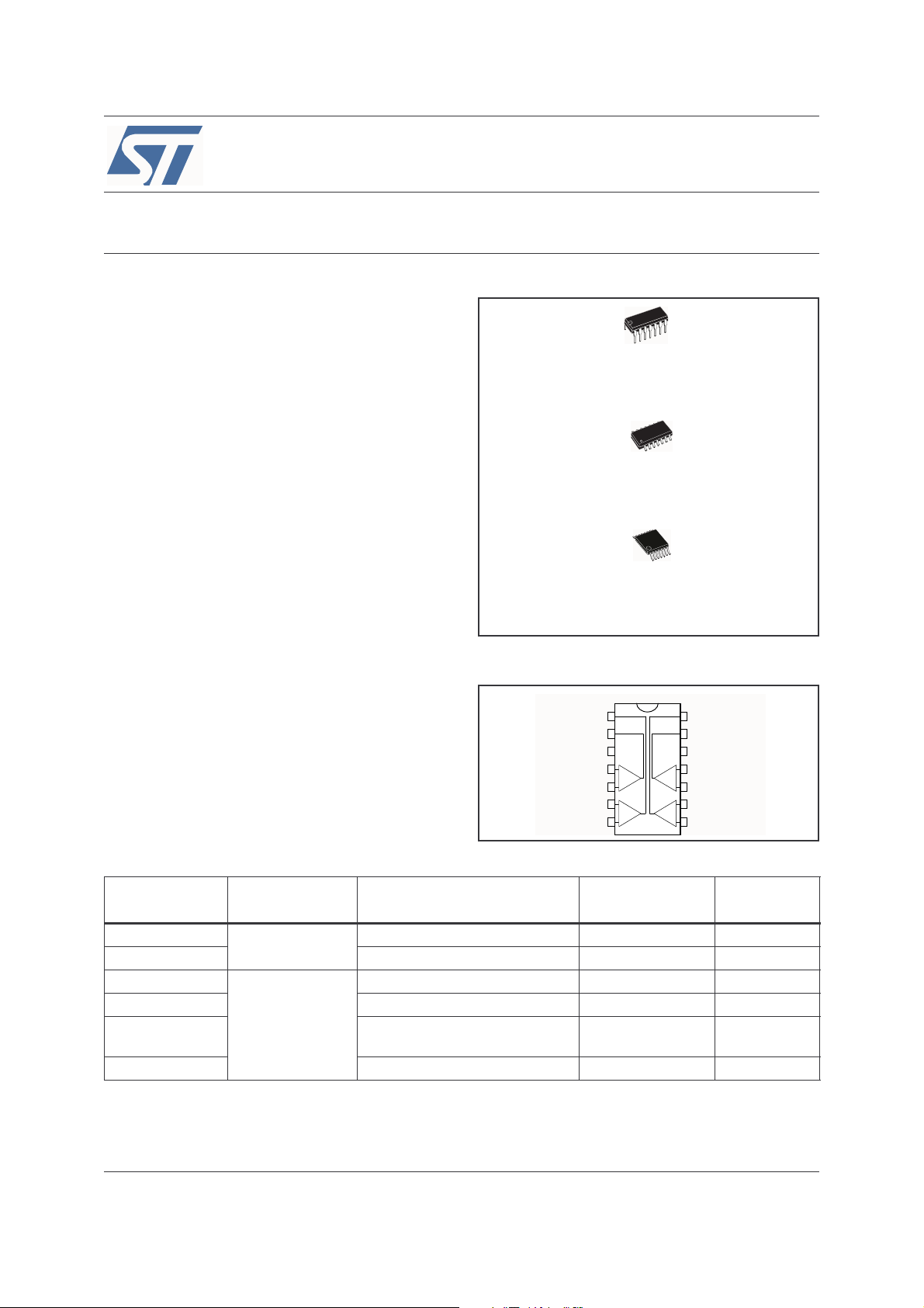
TS339
N
DIP14
(Plastic Package)
D
SO14
(Plastic Micropackage)
P
TSSOP14
(Thin Shrink Small Outline Package)
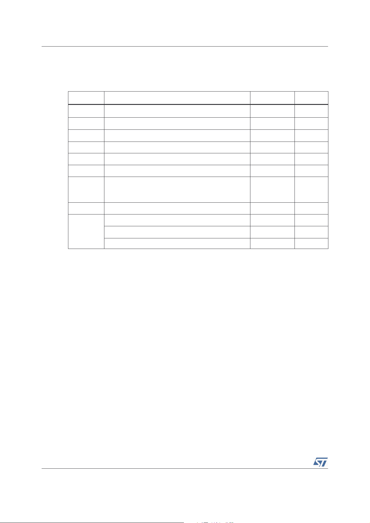
Pin Connection (top view)
Output 2
Output 1
V
Inverting Input 1
Non-inverting Input 1
Inverting Input 2
Non-inverting Input 2
1
2
+
3
CC
4
-
+
5
6
-
+
7
+
-
+
-
14
Output 3
13
Output 4
12
V
CC
11
Non-inverting Input 4
10
Inverting Input 4
9
Non-inverting Input 3
Inverting Input 3
8
-
Order Codes
Par t Nu mber
TS339CN
TS339CD/CDT SO-14 Tube or Tape & Reel S339C
TS339IN
Temperature
Range
0°C, +70°C
Package Packaging Marking
DIP14 Tube TS339CN
DIP14 Tube TS339IN
TS339ID/IDT SO-14 Tube or Tape & Reel S339I
TS339IPT
-40°C, +125°C
(Thin Shrink Outline Package)
TSSOP14
Tape & Reel S339I
TS339IYD/IYDT SO-14 (automotive grade level) Tube or Tape & Reel S339IY
Rev 2
August 2005 1/9
www.st.com
9
Absolute Maximum Ratings TS339
1 Absolute Maximum Ratings
Table 1. Key parameters and their absolute maximum ratings
Symbol Parameter Value Unit
V
CC
V
V
V
I
I
p
T
stg
ESD
+
Supply Voltage
id
o
o
F
Differential Input Voltage
Input Voltage
i
Output Voltage 18 V
Output Current 20 mA
Forward Current in ESD Protection Diodes on Inputs
Power Dissipation
d
SO14
TSSOP14
Storage Temperature Range -65 to +150 °C
HBM: Human Body Model
MM: Machine Model
(3)
(1)
(5)
DIP14
(7)
(2)
(6)
(4)
18 V
±18 V
18 V
50 mA
1500
830
710
50 V
40 V
mW
CDM: Charged Device Model 800 V
1. All voltage values, except differential voltage, are with respect to network ground terminal.
2. Differential voltages are the non-inverting input terminal with respect to the inverting input terminal.
3. Excursions of input voltages may exceed the power supply level. As long as the common mode voltage
[V
However, the maximum current through the ESD diodes (IF) of the input stage must strictly be observed.
4. Guaranteed by design.
5. Pd is calculated with T
R
R
R
6. Human body model, 100pF discharged through a 1.5kΩ resistor into pin of device.
7. Machine model ESD, a 200pF cap is charged to the specified voltage, then discharged directly into the IC with
no external series resistor (internal resistor < 5Ω), into pin to pin of device.
+
=(V
icm
= 80 °C/W for DIP14 package
thja
= 150 °C/W for SO14 package
thja
= 175°C/W for TSSOP14 package
thja
-
+ V
in
)/2] remains within the specified range, the comparator will provide a stable output state.
in
= +25°C, Tj = +150°C and
amb
2/9
TS339 Typical Application Schematics
2 Typical Application Schematics
Figure 1. Schematic diagram (for 1/4 TS339)
V+
CC
T
T
1
T
2
T
9
10
T
17
R
1
Input - Input +
TT
34
T
8
T
5
T
T
6
7
T
11
TT
14 15
T
12
T
13
T
16
V-
CC
T
18
Output
T
20
T
19
3/9

Electrical Characteristics TS339
3 Electrical Characteristics
Table 2. V
CC
+
= 3V, V
CC
-
= 0V, T
= 25°C (unless otherwise specified)
amb
Symbol Parameter Min. Typ. Max. Unit
max.
max.
max.
max
(1)
5
mV
6.5
(2)
1
300
2)
1
600
+
V
0
0
-1.2
CC
+
V
-1.5
CC
70
70
V
io
I
io
I
ib
V
icm
CMR
SVR
Input Offset Voltage
Vic = 1.5V
T
min
. ≤ T
amb
≤ T
Input Offset Current
Vic = 1.5V
T
min
. ≤ T
amb
≤ T
Input Bias Current
Vic = 1.5V
T
min
. ≤ T
amb
≤ T
Input Common Mode Voltage Range
T
min
. ≤ T
amb
≤ T
Common-mode Rejection Ratio
V
= V
ic
icm min.
Supply Voltage Rejection Ratio
+
= 3V to 5V
V
CC
High Level Output Current
V
I
OH
= +1V, VOH = 3V
id
T
min
. ≤ T
amb
≤ T
max.
240
1000
Low Level Output Voltage
V
V
OL
= -1V, IOL = +6mA
id
T
min
. ≤ T
amb
≤ T
max.
400 550
800
mV
Supply Current (each comparator)
No load - Outputs low
I
CC
T
min
. ≤ T
amb
≤ T
max.
92025µA
Response Time Low to High
V
t
PLH
= 0V, f = 10kHz, T
ic
= 5mV
TTL Input
min
. ≤ T
amb
≤ T
= 50pF, Overdrive
maxCL
1.5
0.7
pA
pA
V
dB
dB
nA
µs
Response Time High to Low
PHL
V
= 0V, f = 10kHz, RL = 5.1kΩ, CL = 50pF, Overdrive = 5mV
ic
t
TTL Input
1. The specified offset voltage is the maximum value required to drive the output up to 2.5V or down to 0.3V.
2. Maximum values including unavoidable inaccuracies of the industrial test.
4/9
2.5
0.08
µs

TS339 Electrical Characteristics
Table 3. V
CC
+
= 5V, V
CC
-
= 0V, T
= 25°C (unless otherwise specified)
amb
Symbol Parameter Min. Typ. Max. Unit
(1)
+
= 5V to 10V
max.
(2)
max.
2)
max.
max
1.4 5
6.5
1
300
1
600
+
V
0
0
-1.2
CC
+
-1.5
V
CC
75
85
V
io
I
io
I
ib
V
icm
CMR
SVR
Input Offset Voltage
V
= 2.5V, V
ic
T
. ≤ T
min
amb
cc
≤ T
Input Offset Current
Vic = 2.5V
T
min
. ≤ T
amb
≤ T
Input Bias Current
Vic = 2.5V
T
min
. ≤ T
amb
≤ T
Input Common Mode Voltage Range
T
min
. ≤ T
amb
≤ T
Common-mode Rejection Ratio
V
= 0V
ic
Supply Voltage Rejection Ratio
+
= +5V to +10V
V
CC
High Level Output Voltage
V
I
OH
= 1V, VOH = +5V
id
T
. ≤ T
min
amb
≤ T
max.
27 40
1000
Low Level Output Voltage
V
V
OL
I
CC
= -1V, IOL = 6mA
id
T
min
. ≤ T
amb
≤ T
max.
Supply Current (each comparator)
No load - Outputs low
T
min
. ≤ T
amb
≤ T
max.
260 400
650
10 20
25
Response Time Low to High
V
= 0V, f = 10kHz, RL = 5.1kΩ, CL = 15pF,
t
Overdrive = 5mV
Overdrive = 10mV
PLH
Overdrive = 20mV
Overdrive = 40mV
TTL Input
ic
1.5
1.2
1.1
0.9
0.8
mV
pA
pA
V
dB
dB
nA
mV
µA
µs
Response Time High to Low
V
= 0V, f = 10kHz, RL = 5.1kΩ, CL = 15pF,
ic
Overdrive = 5mV
t
Overdrive = 10mV
PHL
Overdrive = 20mV
Overdrive = 40mV
TTL Input
Fall t ime
t
f
f = 10kHz, C
1. The specified offset voltage is the maximum value required to drive the output up to 4.5V or down to 0.3V.
2. Maximum values including unavoidable inaccuracies of the industrial test.
= 50pF, RL = 5.1kΩ, Overdrive 50mV
L
2.5
1.9
1.2
0.8
0.08
30
µs
ns
5/9

Package Mechanical Data TS339
4 Package Mechanical Data
In order to meet environmental requirements, ST offers these devices in ECOPACK® packages.
These packages have a Lead-free second level interconnect. The category of second level
interconnect is marked on the package and on the inner box label, in compliance with JEDEC
Standard JESD97. The maximum ratings related to soldering conditions are also marked on
the inner box label. ECOPACK is an ST trademark. ECOPACK specifications are available at:
www.st.com
4.1 DIP14 Package
.
Plastic DIP-14 MECHANICAL DATA
DIM.
a1 0.51 0.020
B 1.39 1.65 0.055 0.065
b 0.5 0.020
b1 0.25 0.010
D 20 0.787
E 8.5 0.335
e 2.54 0.100
e3 15.24 0.600
F 7.1 0.280
I 5.1 0.201
L 3.3 0.130
Z 1.27 2.54 0.050 0.100
MIN. TYP MAX. MIN. TYP. MAX.
mm. inch
6/9
P001A

TS339 Package Mechanical Data
4.2 SO-14 Package
SO-14 MECHANICAL DATA
DIM.
A 1.75 0.068
a1 0.1 0.2 0.003 0.007
a2 1.65 0.064
b 0.35 0.46 0.013 0.018
b1 0.19 0.25 0.007 0.010
C 0.5 0.019
c1 45˚ (typ.)
D 8.55 8.75 0.336 0.344
E 5.8 6.2 0.228 0.244
e 1.27 0.050
e3 7.62 0.300
F 3.8 4.0 0.149 0.157
G 4.6 5.3 0.181 0.208
L 0.5 1.27 0.019 0.050
M 0.68 0.026
S˚ (max.)
MIN. TYP MAX. MIN. TYP. MAX.
mm. inch
8
PO13G
7/9

Package Mechanical Data TS339
4.3 TSSOP14 Package
TSSOP14 MECHANICAL DATA
DIM.
A 1.2 0.047
A1 0.05 0.15 0.002 0.004 0.006
A2 0.8 1 1.05 0.031 0.039 0.041
b 0.19 0.30 0.007 0.012
c 0.09 0.20 0.004 0.0089
D 4.9 5 5.1 0.193 0.197 0.201
E 6.2 6.4 6.6 0.244 0.252 0.260
E1 4.3 4.4 4.48 0.169 0.173 0.176
e 0.65 BSC 0.0256 BSC
K0˚ 8˚0˚ 8˚
L 0.45 0.60 0.75 0.018 0.024 0.030
A
MIN. TYP MAX. MIN. TYP. MAX.
A2
A1
mm. inch
b
e
c
K
L
E
D
PIN 1 IDENTIFICATION
1
8/9
E1
0080337D

TS339 Revision History
5 Revision History
Date Revision Changes
Jan. 2003 1 Initial release.
Aug. 2005 2
1 - PPAP references inserted in the datasheet see
on page 1
2 - ESD protection inserted in
absolute maximum ratings on page 2
.
Table 1: Key parameters and their
.
Table : Order Codes
Information furnished is believed to be accurate and reliable. However, STMicroelectronics assumes no responsibility for the consequences
of use of such information nor for any infringement of patents or other rights of third parties which may result from its use. No license is
granted by implication or otherwise under any patent or patent rights of STMicroelectronics. Specifications mentioned in this publication are
subject to change without notice. This publication supersedes and replaces all information previously supplied. STMicroelectronics products
are not authorized for use as critical components in life support devices or systems without express written approval of STMicroelectronics.
The ST logo is a registered trademark of STMicroelectronics.
All other names are the property of their respective owners
© 2005 STMicroelectronics - All rights reserved
STMicroelectronics group of companies
Australia - Belgium - Brazil - Canada - China - Czech Republic - Finland - France - Germany - Hong Kong - India - Israel - Italy - Japan -
Malaysia - Malta - Morocco - Singapore - Spain - Sweden - Switzerland - United Kingdom - United States of America
www.st.com
9/9
 Loading...