


查询TS321AID/AIDT供应商
■ Large output voltage swing:
■ 0 to 3.5V min. (@V
CC
= 5V)
■ Low supply current: 500µA
■ Low input bias current: 20nA
■ Low input offset voltage: 2mV max.
■ Wide power supply range:
■ Single supply: +3V to +30V
■ Dual supplies: ±1.5V to ±15V
■ Stable with high capacitive loads
Description
The TS321 is intended for cost-sensitive
applications where space saving is of great
importance. This bipolar op-amp offers the
benefits of a reduced component size (SOT23-5
package), with specifications that match (or are
better) industry standard devices (like the popular
LM358A, LM324, etc.). The TS321 has an input
common mode range (V
and therefore can be employed in single supply
applications.
) that includes ground,
icm
TS321
Low Power Single Operational Amplifier
D
SO-8
(Plastic Micropackage
L
SOT23-5
(Plastic Package)
Pin connections (top view)
N.C.
8
7
V
6
Output
N.C.
+
V
5
CC
Inverting input
4
+
CC
Inverting input
Non-inverting input
Output
V
CC
Non-inverting input
N.C.
1
2
-
+
3
V
45
-
CC
1
-
2
3
Order Codes
Part Number
TS321ILT
TS321ID/IDT SO8 Tube or Tape & Reel 321I
TS321AILT SOT23-5L Tape & Reel K402
TS321AID/AIDT SO8 Tube or Tape & Reel 321AI
TS321IYLT
TS321AIYLT
TS321IYD/IYDT
TS321AIYD/AIYDT
December 2005 Rev. 4 1/12
Temperature
Range
-40°C, +125°C
Package Packaging Marking
SOT23-5L Tape & Reel K401
K406
SOT23-5L (automotive grade level) Tape & Reel
SO-8 (automotive grade level) Tube or Tape & Reel
www.st.com
12
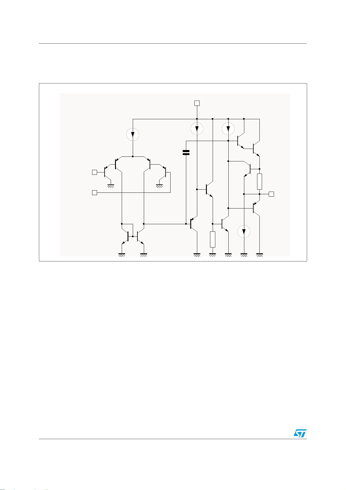
Typical Application Schematics TS321
t
1 Typical Application Schematics
Figure 1. Typical application schematics
V
CC
Inverting
input
Non-inverting
input
Q2
Q8 Q9
6mA
Q3
A
4
m
C
C
Q4Q1
Q10
Q11
100
A
m
Q12
Q5
Q7
50
m
Q13
A
Q6
R
SC
GND
Outpu
2/12
TS321 Absolute Maximum Ratings
2 Absolute Maximum Ratings
Table 1. Key parameters and their absolute maximum ratings
Symbol Parameter Value Unit
V
Supply Voltage ±16 to 32 V
CC
Vi Input Voltage -0.3 to +32 V
V
T
T
R
Differential Input Voltage +32 V
id
Output Short-circuit Duration - note
I
Input Current - note
in
Operating Free Air Temperature Range -40 to +125 °C
oper
Storage Temperature Range -65 to +150 °C
stg
(2)
Thermal Resistance Junction to Ambient
SOT23-5
thja
(1)
(3)
SO8
Infinite
50 mA
250
125
°C/W
Thermal Resistance Junction to Case
R
ESD
1. Short-circuits from the output to VCC can cause excessive heating if VCC > 15V. The maximum output current is
approximately 40mA independent of the magnitude of VCC.
2. This input current only exists when the voltage at any of the input leads is driven negative. It is due to the collector-base
junction of the input PNP transistor becoming forward biased and thereby acting as input diodes clamps. In addition to this
diode action, there is also NPN parasitic action on the IC chip. This transistor action can cause the output voltages of the
Op-amps to go to the V
negative. This is not destructive and normal output will set up again for input voltage higher than -0.3V.
3. Short-circuits can cause excessive heating. Destructive dissipation can result from simultaneous short-circuit on all
amplifiers. All values are typical.
4. Human body model, 100pF discharged through a 1.5kΩ resistor into pin of device.
5. Machine model ESD, a 200pF cap is charged to the specified voltage, then discharged directly into the IC with no external
series resistor (internal resistor < 5Ω), into pin to pin of device.
SOT23-5
thjc
SO8
HBM: Human Body Model
MM: Machine Model
81
40
(4)
(5)
voltage level (or to ground for a large overdrive) for the time duration than an input is driven
CC
300 V
200 V
°C/W
3/12

Electrical Characteristics TS321
3 Electrical Characteristics
Table 2. V
+
= +5V, V
cc
-
= Ground, Vo = 1.4V, T
cc
= +25°C (unless otherwise specified)
amb
Symbol Parameter Conditions Min. Typ. Max. Unit
0.5 4
2
5
mV
3
230
50
20 150
200
nA
nA
5025100 V/mV
dB
500
600
600
800
900
900
µA
1000
0
0
VCC -1.5
V
-2
CC
dB
mA
10
12
26
27
20
50
27
28
mA
µA
V
I
io
I
ib
A
vd
SVR
I
CC
V
icm
CMR
I
source
I
sink
I
o
V
OH
T
= +25°C
amb
TS321A
Input Offset Voltage
io
(1)
T
min.
≤ T
amb
≤ T
max.
TS321A
= +25°C
T
Input Offset Current
Input Bias Current
(2)
Large Signal Voltage
Gain
Supply Voltage
Rejection Ratio
Supply Current, no load
Common Mode Input
Voltage Range
(3)
Common Mode
Rejection Ratio
Output Current Source
Output Sink Current
amb
T
≤ T
min.
T
= +25°C
amb
T
≤ T
min.
+
V
= +15V, RL = 2kΩ, Vo = 1.4V to 11.4V
CC
T
= +25°C
amb
T
≤ T
min.
R
≤ 10kΩ
s
+
= 5 to 30V
V
CC
T
= +25°C 65 110
amb
T
= +25°C, VCC = +5V
amb
V
= +30V
CC
T
≤ T
min.
V
= +30
CC
V
= +30V
CC
= +25°C
T
amb
T
≤ T
min.
R
≤ 10kΩ
s
= +25°C 65 85
T
amb
= +1V
V
id
= +15V, Vo = +2V 20 40
V
CC
V
= -1V
id
= +15V, Vo = +2V
V
CC
V
= +15V, Vo = +0.2V
CC
amb
amb
amb
amb
amb
≤ T
≤ T
≤ T
≤ T
≤ T
max.
max
max.
, VCC = +5V
max.
max.
Short Circuit to Ground VCC = +15V 40 60 mA
V
= +30V
CC
= +25°C, RL = 2kΩ
T
amb
High Level Output
Voltage
T
≤ T
min.
T
= +25°C, RL = 10kΩ
amb
T
≤ T
min.
amb
amb
≤ T
≤ T
max.
max.
25.5
26.5
VCC = +5V, RL = 2kΩ
T
= +25°C
amb
T
≤ T
min.
R
= 10kΩ
V
Low Level Output
OL
Voltage
T
T
L
amb
min.
= +25°C
≤ T
amb
amb
≤ T
≤ T
max.
max.
3.5
3
515
20
mV
V
V
4/12

TS321 Electrical Characteristics
Table 2. V
+
= +5V, V
cc
-
= Ground, Vo = 1.4V, T
cc
= +25°C (unless otherwise specified)
amb
Symbol Parameter Conditions Min. Typ. Max. Unit
V
= +15V, Vi = 0.5 to 3V, RL = 2kΩ,
SR Slew Rate
GBP Gain Bandwith Product
CC
C
= 100pF, T
L
= 30V, f = 100kHz, T
V
CC
V
= 10mV, RL = 2kΩ, CL = 100pF
in
= +25°C, unity gain
amb
amb
= +25°C,
0.4 V/µs
0.8 MHz
φm Phase Margin 60 Degrees
THD
1. Vo = 1.4V, Rs = 0W, 5V < VCC+ < 30V, 0 < Vic < VCC+ - 1.5V
2. The direction of the input current is out of the IC. This current is essentially constant, independent of the state of the output
3. The input common-mode voltage of either input signal voltage should not be allowed to go negative by more than 0.3V.
Total Harmonic
Distortion
Equivalent Input Noise
en
Voltage
so no loading change exists on the input lines.
The upper end of the common-mode voltage range is V
damage.
f = 1kHz, A
C
= 100pF, T
L
f = 1kHz, R
= 20dB, RL = 2kΩ, Vo = 2Vpp,
V
= +25°C, VCC = 30V
amb
= 100Ω, VCC = 30V 40
s
+ - 1.5V, but either or both inputs can go to +32V without
CC
0.015 %
nV
-----------Hz
5/12

Electrical Characteristics TS321
Figure 2. ICC = f(t) Figure 3. AC coupled inverting amplifier
R
f
100k
W
R1
C
10k
W
I
R
B
6.2k
e
I
R2
~
100k
V
W
CC
C1
10
F
m
100k
W
R3
W
R
f
A = -
V
R1
(as shown A = -10)
V
C
o
0
e
o
R
L
10k
W
2V
PP
Figure 4. Non-inverting DC gain Figure 5. AC coupled non-inverting amplifier
A
W
10k
e
O
+5V
(V)
O
e
10k
R1
1/4
TS324
R2
W
1M
W
0
Figure 6. DC summing amplifier
e
100k
100k
W
100k
W
W
1
e
2
R2
= 1 +
V
R1
(As shown = 101)
e
O
A
V
e
(mV)
I
C1
.1mF
R1
100k
C
I
e
I
R3
1M
~
C2
10mF
R2
1M
W
W
100k
100k
6.2k
R4
R5
W
R
B
W
W
V
CC
W
R2
A = 1 +
V
(as shown A = 11)
R1
V
C
o
0
e
o
R
L
10k
W
2V
PP
e
100k
100k
W
100k
W
W
3
e
4
6/12

TS321 Macromodel
4 Macromodel
Note: Please consider following remarks before using this macromodel:
All models are a trade-off between accuracy and complexity (i.e. simulation time).
Macromodels are not a substitute to breadboarding; rather, they confirm the validity of a
design approach and help to select surrounding component values.
A macromodel emulates the NOMINAL performance of a TYPICAL device within
SPECIFIED OPERATING CONDITIONS (i.e. temperature, supply voltage, etc.). Thus the
macromodel is often not as exhaustive as the datasheet, its goal is to illustrate the main
parameters of the product.
Data issued from macromodels used outside of its specified conditions (Vcc, Temperature,
etc) or even worse: outside of the device operating conditions (Vcc, Vicm, etc) are not
reliable in any way.
** Standard Linear Ics Macromodels, 1993.
** CONNECTIONS :
* 1 INVERTING INPUT
* 2 NON-INVERTING INPUT
* 3 OUTPUT
* 4 POSITIVE POWER SUPPLY
* 5 NEGATIVE POWER SUPPLY
.SUBCKT TS321 1 2 3 4 5
***************************
.MODEL MDTH D IS=1E-8 KF=3.104131E-15 CJO=10F
* INPUT STAGE
CIP 2 5 1.000000E-12
CIN 1 5 1.000000E-12
EIP 10 5 2 5 1
EIN 16 5 1 5 1
RIP 10 11 2.600000E+01
RIN 15 16 2.600000E+01
RIS 11 15 2.003862E+02
DIP 11 12 MDTH 400E-12
DIN 15 14 MDTH 400E-12
VOFP 12 13 DC 0
VOFN 13 14 DC 0
IPOL 13 5 1.000000E-05
CPS 11 15 3.783376E-09
DINN 17 13 MDTH 400E-12
VIN 17 5 0.000000e+00
DINR 15 18 MDTH 400E-12
VIP 4 18 2.000000E+00
FCP 4 5 VOFP 3.400000E+01
FCN 5 4 VOFN 3.400000E+01
FIBP 2 5 VOFN 2.000000E-03
FIBN 5 1 VOFP 2.000000E-03
* AMPLIFYING STAGE
FIP 5 19 VOFP 3.600000E+02
FIN 5 19 VOFN 3.600000E+02
RG1 19 5 3.652997E+06
RG2 19 4 3.652997E+06
CC 19 5 6.000000E-09
7/12

Macromodel TS321
DOPM 19 22 MDTH 400E-12
DONM 21 19 MDTH 400E-12
HOPM 22 28 VOUT 7.500000E+03
VIPM 28 4 1.500000E+02
HONM 21 27 VOUT 7.500000E+03
VINM 5 27 1.500000E+02
EOUT 26 23 19 5 1
VOUT 23 5 0
ROUT 26 3 20
COUT 3 5 1.000000E-12
DOP 19 25 MDTH 400E-12
VOP 4 25 2.242230E+00
DON 24 19 MDTH 400E-12
VON 24 5 7.922301E-01
.ENDS
Table 3. V
Symbol Conditions Value Unit
+
= 3V, VCC- = 0V, RL, CL connected to V
CC
CC/2
, T
= 25°C (unless otherwise specified)
amb
V
io
A
vd
I
CC
V
icm
V
OH
V
OL
I
os
GBP R
SR R
∅mR
RL = 2kΩ 100 V/mV
No load, per operator 300 µA
RL = 2kΩ +3.5 V
RL = 2kΩ 5mV
Vo = 0V 40 mA
= 2kΩ, CL = 100pF 0.8 MHz
L
= 2kΩ, CL = 100pF 0.4 V/µs
L
= 2kΩ, CL = 100pF 60 Degrees
L
0mV
0 to +3.5 V
8/12

TS321 Macromodel
Figure 7. ICC = f(t) Figure 8. AC coupled inverting amplifier
R
f
100k
W
R1
C
10k
W
I
R
B
6.2k
e
I
R2
~
100k
V
W
CC
C1
10
F
m
100k
W
R3
W
R
f
A = -
V
R1
(as shown A = -10)
V
C
o
0
e
o
R
L
10k
W
2V
PP
Figure 9. Non-inverting DC gain Figure 10. AC coupled non-inverting amplifier
A
W
10k
e
O
+5V
(V)
O
e
10k
R1
1/4
TS324
R2
W
1M
W
0
Figure 11. DC summing amplifier
e
100k
100k
W
100k
W
W
1
e
2
R2
= 1 +
V
R1
(As shown = 101)
e
O
A
V
e
(mV)
I
C1
.1mF
R1
100k
C
I
e
I
R3
1M
~
C2
10mF
R2
1M
W
W
100k
100k
6.2k
R4
R5
W
R
B
W
W
V
CC
W
R2
A = 1 +
V
(as shown A = 11)
R1
V
C
o
0
e
o
R
L
10k
W
2V
PP
e
100k
100k
W
100k
W
W
3
e
4
9/12

Package Mechanical Data TS321
5 Package Mechanical Data
In order to meet environmental requirements, ST offers these devices in ECOPACK®
packages. These packages have a Lead-free second level interconnect. The category of
second level interconnect is marked on the package and on the inner box label, in
compliance with JEDEC Standard JESD97. The maximum ratings related to soldering
conditions are also marked on the inner box label. ECOPACK is an ST trademark.
ECOPACK specifications are available at: www.st.com
5.1 SO-8 Package
SO-8 MECHANICAL DATA
.
DIM.
A 1.35 1.75 0.053 0.069
A1 0.10 0.25 0.04 0.010
A2 1.10 1.65 0.043 0.065
B 0.33 0.51 0.013 0.020
C 0.19 0.25 0.007 0.010
D 4.80 5.00 0.189 0.197
E 3.80 4.00 0.150 0.157
e 1.27 0.050
H 5.80 6.20 0.228 0.244
h 0.25 0.50 0.010 0.020
L 0.40 1.27 0.016 0.050
k ˚ (max.)
ddd 0.1 0.04
MIN. TYP MAX. MIN. TYP. MAX.
mm. inch
8
10/12
0016023/C

TS321 Package Mechanical Data
5.2 SOT23-5 Package
SOT23-5L MECHANICAL DATA
DIM.
A 0.90 1.45 35.4 57.1
A1 0.00 0.15 0.0 5.9
A2 0.90 1.30 35.4 51.2
b 0.35 0.50 13.7 19.7
C 0.09 0.20 3.5 7.8
D 2.80 3.00 110.2 118.1
E 2.60 3.00 102.3 118.1
E1 1.50 1.75 59.0 68.8
e.95 37.4
e1 1.9 74.8
L 0.35 0.55 13.7 21.6
MIN. TYP MAX. MIN. TYP. MAX.
mm. mils
0
11/12

Revision history TS321
6 Revision history
Table 4. Document revision history
Date Revision Changes
June 2001 1 – Initial release.
July 2005 2
Sept. 2005 3
Dec. 2005 4
– PPAP references inserted in the datasheet see table order
codes table
on page 1
– ESD protection inserted in
.
Table 1 on page 3
– Correction of errors in package names and markings in order
codes table
on page 1
.
– Minor grammatical and formatting corrections.
– Missing PPAP references inserted see order codes table
page 1
.
on
– Thermal Resistance Junction to Ambient and Thermal
Resistance Junction to Case information added in
page 3
.
– Macromodel updated see
Chapter 4: Macromodel
Table 1 on
.
Information furnished is believed to be accurate and reliable. However, STMicroelectronics assumes no responsibility for the consequences
of use of such information nor for any infringement of patents or other rights of third parties which may result from its use. No license is
granted by implication or otherwise under any patent or patent rights of STMicroelectronics. Specifications mentioned in this publication are
subject to change without notice. This publication supersedes and replaces all information previously supplied. STMicroelectronics products
are not authorized for use as critical components in life support devices or systems without express written approval of STMicroelectronics.
The ST logo is a registered trademark of STMicroelectronics.
All other names are the property of their respective owners
© 12 STMicroelectronics - All rights reserved
STMicroelectronics group of companies
Australia - Belgium - Brazil - Canada - China - Czech Republic - Finland - France - Germany - Hong Kong - India - Israel - Italy - Japan -
Malaysia - Malta - Morocco - Singapore - Spain - Sweden - Switzerland - United Kingdom - United States of America
www.st.com
12/12
 Loading...