


TS27M4C, TS27M4I, TS27M4M
Inverting Input 2
Non-inverting Input 2
Non-inverting Input 1
CC
V
-
CC
V
1
2
3
4
8
5
6
7
9
10
11
12
13
14
+
Output 3
Output 4
Non-inverting Input 4
Inverting Input 4
Non-inverting Input 3
Inverting Input 3
-
+
-
+
-
+
-
+
Output 1
Inverting Input 1
Output 2
Precision low power CMOS quad operational amplifiers
Features
■ Low power consumption: 150 µA/op
■ Output voltage can swing to ground
■ Excellent phase margin on capacitive loads
■ Unity gain stable
■ Two input offset voltage selections
Description
These devices are low cost, low power quad
operational amplifiers designed to operate with
single or dual supplies. These operational
amplifiers use the ST silicon gate CMOS process
allowing an excellent consumption-speed ratio.
These series are ideally suited for low
consumption applications.
Three power consumptions are available thus
offering the best consumption-speed ratio for your
application:
■ ICC = 10 µA/amp: TS27L4 (very low power)
■ ICC = 150 µA/amp: TS27M4 (low power)
■ ICC = 1 mA/amp: TS274 (standard)
DIP14
(Plastic package)
SO14
(Plastic micropackage)
TSSOP14
(Thin shrink small outline package)
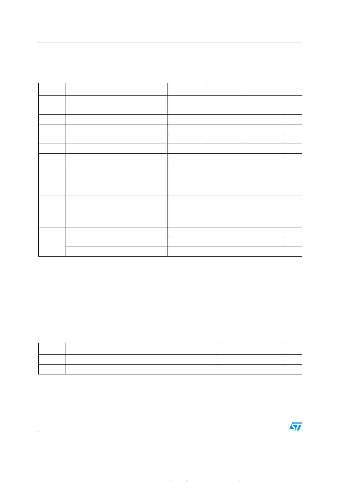
Pin connections (top view)
These CMOS amplifiers offer very high input
impedance and extremely low input currents. The
major advantage versus JFET devices is the very
low input currents drift with temperature (see
Figure 4 on page 7).
September 2008 Rev 2 1/14
www.st.com
14

Circuit schematics TS27M4C, TS27M4I, TS27M4M
E
E
Input
differential
Second
stage
Output
stage
Output
CC
V
CC
V
Current
source
x I
1 Circuit schematics
Figure 1. Block diagram
2/14

TS27M4C, TS27M4I, TS27M4M Circuit schematics
Figure 2. Schematic diagram (for 1/4 TS27M4)
15
T
12
T
10
T
11
T
8
T
6
T
Output
7
T
16
T
14
T
13
T
9
T
R1
C1
Input
2
T
5
CC
V
T
1
T
4
T
3
T
27
T
26
T
25
T
24
T
Inpu t
28
T
23
T
2
R
18
T
17
T
19
T
29
T
22
T
21
T
20
T
CC
V
3/14
Absolute maximum ratings and operating conditions TS27M4C, TS27M4I, TS27M4M
2 Absolute maximum ratings and operating conditions
Table 1. Absolute maximum ratings (AMR)
Symbol Parameter TS27M4C/AC TS27M4I/AI TS27M4M/AM Unit
(3)
(1)
18 V
(2)
±18 V
-0.3 to 18 V
+
≥ 15V ±30 mA
CC
(4)
105
100
80
(4)
31
32
33
(5)
(6)
(7)
1kV
100 V
1.5 kV
+ Supply voltage
V
CC
T
T
V
V
I
I
oper
Differential input voltage
id
Input voltage
in
Output current for V
o
Input current ±5 mA
in
Operating free-air temperature range 0 to +70 -40 to +125 -55 to +125 °C
Storage temperature range -65 to +150 °C
stg
Thermal resistance junction to ambient
R
thja
SO-14
TSSOP14
DIP14
Thermal resistance junction to case
R
thjc
SO-14
TSSOP14
DIP14
HBM: human body model
ESD
MM: machine model
CDM: charged device model
°C/W
°C/W
1. All values, except differential voltage are with respect to network ground terminal.
2. Differential voltages are the non-inverting input terminal with respect to the inverting input terminal.
3. The magnitude of the input and the output voltages must never exceed the magnitude of the positive supply voltage.
4. Short-circuits can cause excessive heating and destructive dissipation. Values are typical.
5. Human body model: a 100 pF capacitor is charged to the specified voltage, then discharged through a 1.5kΩ resistor
between two pins of the device. This is done for all couples of connected pin combinations while the other pins are floating.
6. Machine model: a 200 pF capacitor is charged to the specified voltage, then discharged directly between two pins of the
device with no external series resistor (internal resistor < 5Ω). This is done for all couples of connected pin combinations
while the other pins are floating.
7. Charged device model: all pins and the package are charged together to the specified voltage and then discharged directly
to the ground through only one pin. This is done for all pins.
Table 2. Operating conditions
Symbol Parameter Value Unit
+
V
CC
V
icm
Supply voltage 3 to 16 V
Common mode input voltage range 0 to V
+
- 1.5 V
CC
4/14

TS27M4C, TS27M4I, TS27M4M Electrical characteristics
3 Electrical characteristics
Table 3. V
+
= +10 V, V
CC
Symbol Parameter
Input offset voltage
VO = 1.4V, Vic = 0V
TS27M4C/I/M
V
io
TS27M4AC/AI/AM
≤ T
T
min
amb
≤ T
max
TS27M4C/I/M
TS27M4AC/AI/AM
DV
Input offset voltage drift 2 2 µV/°C
io
Input offset current note
I
Vic = 5V, VO = 5V
io
T
≤ T
amb
≤ T
max
min
Input bias current
I
Vic = 5V, VO = 5V
ib
T
≤ T
amb
≤ T
max
min
High level output voltage
V
V
Vid = 100mV, RL = 100kΩ
OH
≤ T
T
min
amb
Low level output voltage
OL
= -100mV
V
id
≤ T
max
Large signal voltage gain
A
vd
GBP
CMR
SVR
= 5V, RL = 100kΩ, Vo = 1V to 6V
V
iC
T
≤ T
amb
≤ T
max
min
Gain bandwidth product
= 40dB, RL = 100kΩ, CL = 100pF, fin = 100kHz
A
v
Common mode rejection ratio
V
= 1V to 7.4V, Vo = 1.4V
iC
Supply voltage rejection ratio
+
V
= 5V to 10V, Vo = 1.4V
CC
Supply current (per amplifier)
I
CC
I
o
= 1, no load, Vo = 5V
A
v
T
≤ T
amb
≤ T
max
min
Output short-circuit current
Vo = 0V, Vid = 100mV
(1)
CC
-
= 0 V, T
(1)
= +25° C (unless otherwise specified)
amb
TS27M4C/AC
Min. Typ. Max. Min. Typ. Max.
1.1
0.9105
12
6.5
1
100
1
150
8.7
8.9 8.7
8.6
50 50 mV
302050 301050
11MHz
65 80 65 80 dB
60 80 60 80 dB
150 200
250
60 60 mA
TS27M4I/AI
TS27M4M/AM
1.1
0.9105
1
1
8.9
8.5
150 200
Unit
mV
12
6.5
pA
200
pA
300
V
V/mV
µA
300
I
sink
SR
Output sink current
Vo = VCC, Vid = -100mV
Slew rate at unity gain
R
= 100kΩ, CL = 100pF, Vi = 3 to 7V
L
45 45 mA
0.6 0.6 V/µs
5/14
 Loading...