

TS27M2, TS27M2A, TS27M2B
Low-power CMOS dual operational amplifiers
Features
■ Wide supply voltage range: 3 to 16 V
■ Ultra-low consumption: 150 µA/op typ
■ Output voltage swing to ground
■ Excellent phase margin on capacitive load
■ Gain bandwidth product: 1 MHz typ
■ Vio down to 2 mV max. (B version)
Description
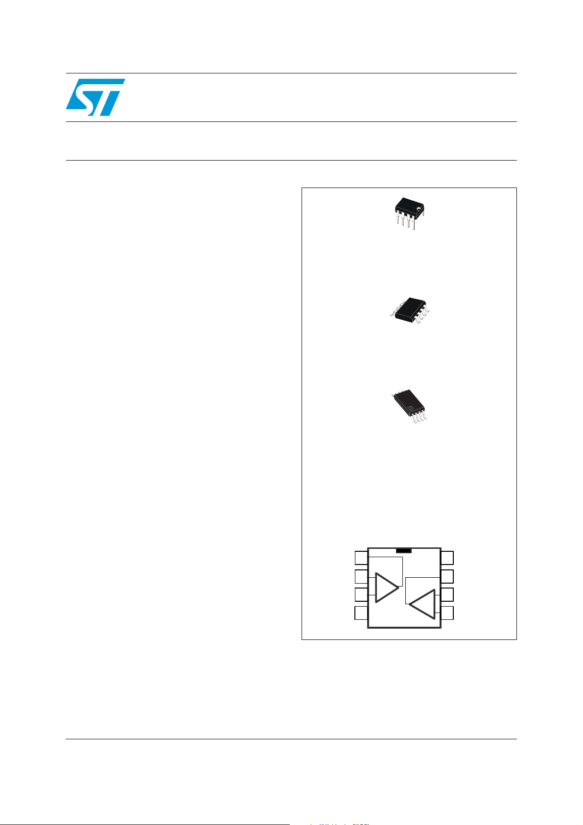
N
DIP8
(Plastic package)
The TS27x2 series are low-cost and low-power
dual operational amplifiers designed to operate
with high-voltage single or dual supplies. These
operational amplifiers use the ST silicon gate
CMOS process, providing an excellent
consumption-speed ratio thanks to three different
power consumptions, making them ideal for lowconsumption applications:
I
= 10 µA/amp: TS27L2 (very low power),
CC
I
= 150 µA/amp: TS27M2 (low power) and
CC
I
= 1 mA/amp: TS272 (high speed)
CC
The devices also offer a very high input
impedance and extremely low input currents.
Their main advantage compared to JFET devices
is the very low input current drift with temperature
(Figure 3).
D
SO-8
(Plastic micropackage)
P
TSSOP8
(Thin shrink small outline package)
Pin connections (top view)
Out1
Out1
In1-
In1-
In1+
In1+
V
V
CC-
CC-
1
1
_
_
2
2
+
+
3
3
4
4
8
8
V
V
CC+
CC+
7
7
Out2
Out2
_
_
+
+
In2-
In2-
6
6
In2+
In2+
5
5
August 2009 Doc ID 2306 Rev 2 1/14
www.st.com
14
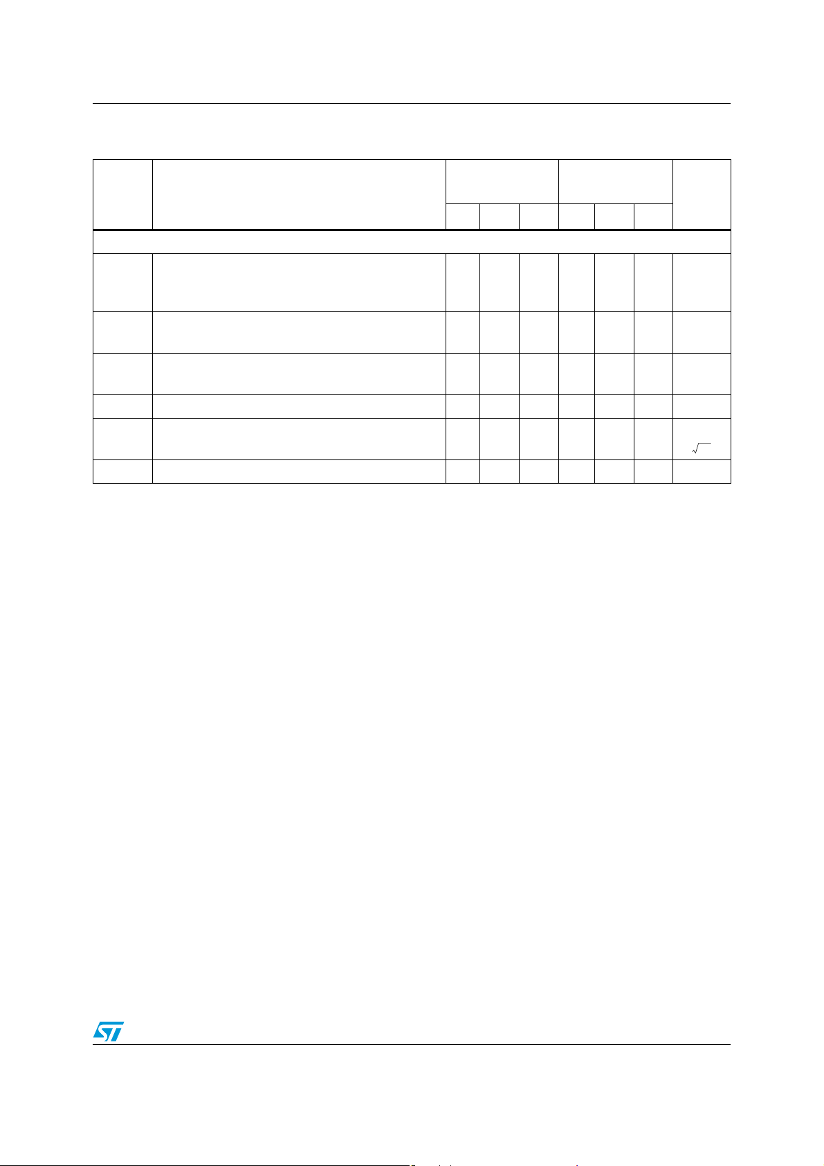
Absolute maximum ratings and operating conditions TS27M2, TS27M2A, TS27M2B
1 Absolute maximum ratings and operating conditions
Table 1. Absolute maximum ratings
Symbol Parameter TS27M2x/Ax/Bx Unit
+
CC
Supply voltage
V
Vid Differential input voltage
Input voltage
V
i
Output current for V
I
o
I
Input current ±5 mA
in
SO-8
(4)(5)
R
thja
DIP8
TSSOP8
(3)
(1)
18 V
(2)
±18 V
-0.3 to 18 V
+
≥ 15V ±30 mA
CC
125
85
120
°C/W
T
Storage temperature range -65 to +150 °C
stg
Maximum junction temperature 150 °C
T
j
HBM: human body model
ESD
MM: machine model
CDM: charged device model
1. All values, except differential voltage are with respect to network ground terminal.
2. Differential voltages are the non-inverting input terminal with respect to the inverting input terminal.
3. The magnitude of the input and the output voltages must never exceed the magnitude of the positive
supply voltage.
4. Short-circuits can cause excessive heating and destructive dissipation.
are typical values.
5. R
th
6. Human body model: a 100 pF capacitor is charged to the specified voltage, then discharged through a
1.5 kΩ resistor between two pins of the device. This is done for all couples of connected pin combinations
while the other pins are floating.
7. Machine model: a 200 pF capacitor is charged to the specified voltage, then discharged directly between
two pins of the device with no external series resistor (internal resistor < 5 Ω). This is done for all couples of
connected pin combinations while the other pins are floating.
8. Charged device model: all pins and the package are charged together to the specified voltage and then
discharged directly to the ground through only one pin. This is done for all pins.
Table 2. Operating conditions
Symbol Parameter
+
V
V
Supply voltage 3 to 16 V
CC
Common mode input voltage
icm
range
(6)
(7)
(8)
500 V
100 V
1.5 kV
Val ue Unit
TS27M2C/AC/BC TS27M2I/AI/BI TS27M2M/AM/BM
0 to V
+
- 1.5 V
CC
Toper
Operating free air temperature
range
0 to +70 -40 to +125 -55 to +125 °C
2/14 Doc ID 2306 Rev 2
TS27M2, TS27M2A, TS27M2B Absolute maximum ratings and operating conditions
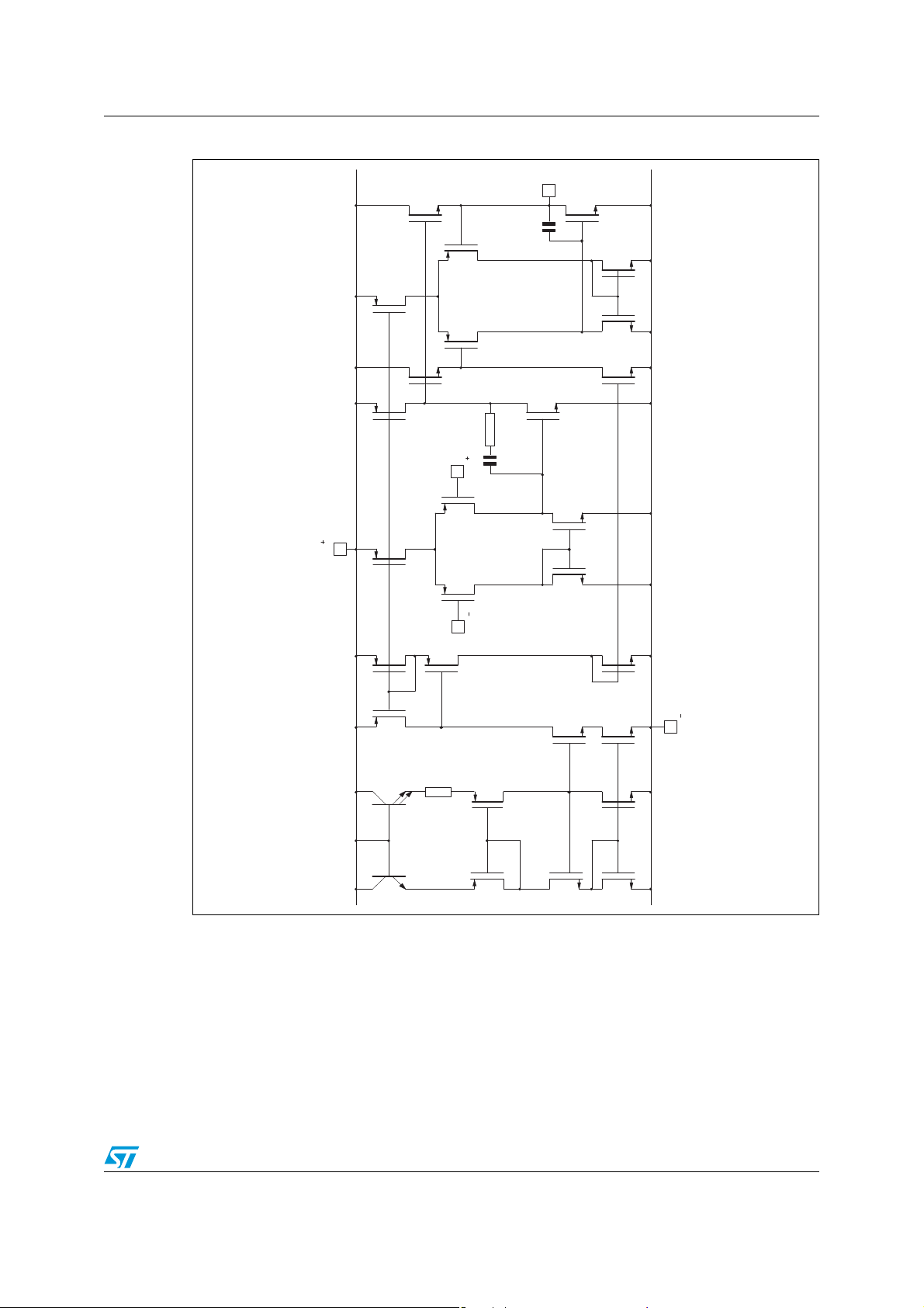
Figure 1. Simplified schematic diagram (for 1/2 TS27M2)
15
T
12
T
10
T
11
T
8
T
6
T
Output
16
T
14
T
13
T
9
T
7
T
R1
C1
Inpu t
2
T
5
CC
V
T
1
T
27
T
Inp u t
28
T
4
T
3
T
29
T
23
22
26
T
2
25
T
24
T
R
18
T
17
T
T
19
T
T
21
T
20
T
CC
V
Doc ID 2306 Rev 2 3/14
Electrical characteristics TS27M2, TS27M2A, TS27M2B
2 Electrical characteristics
Table 3. Electrical characteristics at VCC+ = +10 V, VCC- = 0 V, T
(unless otherwise specified)
Symbol Parameter
DC performance
Input offset voltage
VO = 1.4 V, Vic = 0 V TS27M2
TS27M2A
V
io
≤ T
amb
≤ T
max
T
min
TS27M2B
TS27M2
TS27M2A
TS27M2B
DV
Input offset voltage drift 2 2 µV/°C
io
≤ T
≤ T
(1)
max
(1)
max
Input offset current
I
io
Vic = 5 V, VO = 5 V
T
Input bias current
I
ib
Vic = 5 V, VO = 5 V
T
min
min
≤ T
≤ T
amb
amb
High level output voltage
V
OH
V
OL
Vid = 100 mV, RL = 100 lΩ
≤ T
amb
≤ T
max
T
min
Low level output voltage
= -100 mV 50 50
V
id
Large signal voltage gain
A
vd
CMR
SVR
= 5 V, RL = 100 kΩ, Vo = 1 V to 6 V
V
iC
T
≤ T
amb
≤ T
max
min
Common mode rejection ratio
= 1V to 7.4V, Vo = 1.4 V 65 80 65 80
V
iC
Supply voltage rejection ratio
+
V
= 5 V to 10 V, Vo = 1.4 V 60 80 60 80
CC
Supply current (per amplifier)
I
CC
I
o
= 1, no load, Vo = 5 V
A
v
T
≤ T
amb
≤ T
max
min
Output short circuit current
Vo = 0 V, Vid = 100 mV
TS27M2xC
Min. Typ. Max. Min. Typ. Max.
1.1
0.9
0.25
1
1
8.7
8.9 8.7
8.6
302050 301050
150 200
45 60 60 mA
= +25° C
amb
10
5
2
12
6.5
3
100
150
250
TS27M2xI
TS27M2xM
0.25
8.5
150 200
1.1
0.9
1
1
8.9
10
5
2
12
6.5
3.5
200
300
300
Unit
mV
pA
pA
V
mV
V/mV
dB
dB
µA
I
sink
Output sink current
Vo = VCC, Vid = -100 mV
4/14 Doc ID 2306 Rev 2
34 45 45 mA
TS27M2, TS27M2A, TS27M2B Electrical characteristics
Table 3. Electrical characteristics at VCC+ = +10 V, VCC- = 0 V, T
(unless otherwise specified) (continued)
Symbol Parameter
AC performance
Gain bandwidth product
GBP
SR
φm
K
OV
e
n
V
o1/Vo2
1. Maximum values including unavoidable inaccuracies of industrial tests.
Av = 40 dB, RL = 100 kΩ, CL = 100 pF,
f
= 100 kHz
in
Slew rate at unity gain
R
= 100 kΩ, CL = 100 pF, Vi = 3 to 7 V
L
Phase margin at unity gain
A
= 40 dB, RL = 100 kΩ, CL = 100 pF
v
Overshoot factor 30 30 %
Equivalent input noise voltage
f = 1 kHz, R
= 100 Ω
s
Channel separation 120 120 dB
TS27M2xC
Min. Typ. Max. Min. Typ. Max.
0.5 1 0.5 1 MHz
0.3 0.6 0.3 0.6 V/μs
45 45 Degrees
38 38
= +25° C
amb
TS27M2xI
TS27M2xM
Unit
nV
-----------Hz
Doc ID 2306 Rev 2 5/14

Typical characteristics TS27M2, TS27M2A, TS27M2B
25 50 75 100 125
AMB
INPUT BIAS CUR RENT, I (pA)
IB
TEMPERATURE, T ( C)
˚
V = 10V
V = 5V
CC
i
100
10
1
5
4
3
2
1
0
-10 -8 -6 -4 -2 0
OH
OUTPUT CURRENT, I (mA)
OUTPUT VOLTAGE, V (V)
OH
AMB
ID
T = 25 C
V = 100mV
˚
V = 5V
V = 3V
CC
CC
20
16
12
8
4
0
-50 -40 -30 -20 -10 0
AMB
ID
˚
T = 25 C
V = 100mV
V = 16V
CC
CC
V = 10V
OUTPUT CURRENT, I (mA)
OH
OH
OUTPUT VOLTAGE, V (V)
1.0
0.8
0.6
0.4
0.2
AMB
i
ID
V = 3V
V = 5V
CC
CC
˚
OUTPUT CURRENT, I (mA)
OL
OL
OUTPUT VOLTAGE, V (V)
0 1 2 3
T = 25 C
V = 0.5V
V = -1V
3
2
1
0 4 8 12 16 20
OUTPUT CURRENT, I (mA)
OL
OUTPUT VOLTAGE, V (V)
OL
AMB
ID
i
T = 25 C
V = 0.5V
V = -1V
˚
CC
V = 10V
CC
V = 16V
3 Typical characteristics
Figure 2. Supply current (each amplifier)
versus supply voltage
200
T = 25 C
AMB
˚
A = 1
CC
150
V
V = V / 2
O CC
μ
100
50
SUPPLY CURRENT, I ( A)
0 4 8 12 16
SUPPLY VOLTAGE, V (V)
CC
Figure 4. High level output voltage versus
high level output current
Figure 3. Input bias current versus free air
temperature
Figure 5. High level output voltage versus
high level output current
Figure 6. Low level output voltage versus low
level output current
6/14 Doc ID 2306 Rev 2
Figure 7. Low level output voltage versus low
level output current

TS27M2, TS27M2A, TS27M2B Typical characteristics
50
40
30
20
10
0
-10
6
10
10
23
10
4
10510
7
10
GAIN (dB)
PHASE (Degrees)
0
45
90
135
180
FREQUENCY, f (Hz)
T = 25˚C
V = 10V
R = 100k
Ω
C = 100pF
A = 100
amb
CC
L
L
VCL
PHASE
GAIN
Phase
Margin
Gain
Bandwidth
Product
+
SUPPLY VOLTAGE, V (V)
CC
0 4 8 12 16
1800
1400
1000
600
200
T = 25˚C
R = 100kΩ
C = 100pF
A = 1
amb
L
L
V
GAIN BANDW. PROD., GBP (kHz)
0 20 40 60 80 100
CAPACITANCE, C (pF)
L
PHASE MARGIN, m (Degrees )
φ
80
70
60
50
40
T = 25˚C
R = 100kΩ
A = 1
V = 10V
amb
L
V
CC
6
300
200
100
0
EQUIVALENT INPUT NOISE
VOLTA GE (n V/VHz )
1
10
100
1000
FREQUENCY (Hz)
= 10 V
= 25˚C
T
am b
V
CC
= 100
Ω
R
S
Figure 8. Open-loop frequency response and
phase shift
Figure 10. Phase margin versus supply
voltage
50
40
φ
T = 25˚C
amb
30
R = 100kΩ
L
C = 100pF
L
A = 1
V
20
PHASE MARGIN, m (Degrees)
0 4 8 12 16
SUPPLY VOLTAGE, V (V)
CC
Figure 9. Gain bandwidth product versus
supply voltage
Figure 11. Phase margin versus capacitive
load
Figure 12. Slew rate versus supply voltage Figure 13. Input voltage noise versus
0.9
s)
μ
0.8
0.7
0.6
0.5
SLEW RATES, SR (V/
0.4
T = 25˚C
amb
R = 100kΩ
L
C = 100pF
L
SR
SR
4 6 8 10 12 14 1
SUPPLY VOLTAGE, V (V)
CC
frequency
Doc ID 2306 Rev 2 7/14

Package information TS27M2, TS27M2A, TS27M2B
4 Package information
In order to meet environmental requirements, ST offers these devices in different grades of
ECOPACK
specifications, grade definitions and product status are available at: www.st.com.
ECOPACK
®
packages, depending on their level of environmental compliance. ECOPACK®
®
is an ST trademark.
8/14 Doc ID 2306 Rev 2

TS27M2, TS27M2A, TS27M2B Package information
4.1 DIP8 package information
Figure 14. DIP8 package mechanical drawing
Table 4. DIP8 package mechanical data
Dimensions
Ref.
Min. Typ. Max. Min. Typ. Max.
A5.330.210
A1 0.38 0.015
A2 2.92 3.30 4.95 0.115 0.130 0.195
b 0.36 0.46 0.56 0.014 0.018 0.022
b2 1.14 1.52 1.78 0.045 0.060 0.070
c 0.20 0.25 0.36 0.008 0.010 0.014
D 9.02 9.27 10.16 0.355 0.365 0.400
E 7.62 7.87 8.26 0.300 0.310 0.325
E1 6.10 6.35 7.11 0.240 0.250 0.280
e 2.54 0.100
eA 7.62 0.300
eB 10.92 0.430
L 2.92 3.30 3.81 0.115 0.130 0.150
Millimeters Inches
Doc ID 2306 Rev 2 9/14

Package information TS27M2, TS27M2A, TS27M2B
4.2 SO-8 package information
Figure 15. SO-8 package mechanical drawing
Table 5. SO-8 package mechanical data
Dimensions
Ref.
Min. Typ. Max. Min. Typ. Max.
A1.750.069
A1 0.10 0.25 0.004 0.010
A2 1.25 0.049
b 0.28 0.48 0.011 0.019
c 0.17 0.23 0.007 0.010
D 4.80 4.90 5.00 0.189 0.193 0.197
E 5.80 6.00 6.20 0.228 0.236 0.244
E1 3.80 3.90 4.00 0.150 0.154 0.157
e 1.27 0.050
h 0.25 0.50 0.010 0.020
L 0.40 1.27 0.016 0.050
L1 1.04 0.040
k1° 8°1° 8°
ccc 0.10 0.004
Millimeters Inches
10/14 Doc ID 2306 Rev 2

TS27M2, TS27M2A, TS27M2B Package information
4.3 TSSOP8 package information
Figure 16. TSSOP8 package mechanical drawing
Table 6. TSSOP8 package mechanical data
Dimensions
Ref.
Min. Typ. Max. Min. Typ. Max.
A1.200.047
A1 0.05 0.15 0.002 0.006
A2 0.80 1.00 1.05 0.031 0.039 0.041
b 0.19 0.30 0.007 0.012
c 0.09 0.20 0.004 0.008
D 2.90 3.00 3.10 0.114 0.118 0.122
E 6.20 6.40 6.60 0.244 0.252 0.260
E1 4.30 4.40 4.50 0.169 0.173 0.177
e 0.65 0.0256
k0° 8°0° 8°
L 0.45 0.60 0.75 0.018 0.024 0.030
L1 1 0.039
aaa 0.10 0.004
Millimeters Inches
Doc ID 2306 Rev 2 11/14

Ordering information TS27M2, TS27M2A, TS27M2B
5 Ordering information
Table 7. Order codes
Part number
TS27M2CD
TS27M2CDT
TS27M2CN DIP8 Tube TS27M2CN
TS27M2CPT TSSOP8
TS27M2ACD
TS27M2ACDT
TS27M2ACN DIP8 Tube S27M2ACN
TS27M2ACPT TSSOP8 Tape & reel 2M2AC
TS27M2BCD
TS27M2BCDT
TS27M2BCN DIP8 Tube S27M2BCN
TS27M2BCPT TSSOP8 Tape & reel 2M2BC
TS27M2ID
TS27M2IDT
TS27M2IN DIP8 Tube TS27M2IN
TS27M2IPT TSSOP8 Tape & reel 27M2I
TS27M2AID
TS27M2AIDT
TS27M2AIN DIP8 Tube S27M2AIN
Temperature
range
0° C to +70° C
-40° C to +125° C
Package Packing Marking
SO-8
SO-8
SO-8
SO-8
SO-8
Tu b e
Tape & reel
Tu b e
Tape & reel
Tu b e
Tape & reel
Tu b e
Tape & reel
Tu b e
Tape & reel
Tu b e
Tape & reel
27M2C
27M2C
27M2AC
27M2BC
27M2I
27M2AI
TS27M2AIPT TSSOP8 Tape & reel 2M2AI
TS27M2BID
TS27M2BIDT
TS27M2BIN DIP8 Tube S27M2BIN
TS27M2BIPT TSSOP8 Tape & reel 2M2BI
12/14 Doc ID 2306 Rev 2
SO-8
Tu b e
Tape & reel
27M2BI

TS27M2, TS27M2A, TS27M2B Revision history
6 Revision history
Table 8. Document revision history
Date Revision Changes
01-Nov-2001 1 Initial release.
Updated document format.
Added ESD and Rthja information in Table 1: Absolute
maximum ratings.
18-Aug-2009 2
Removed block diagram.
Added minimum values for Io, GBP and SR parameters in
Ta bl e 3.
Added order codes in Ta b le 7 .
Doc ID 2306 Rev 2 13/14

TS27M2, TS27M2A, TS27M2B
Please Read Carefully:
Information in this document is provided solely in connection with ST products. STMicroelectronics NV and its subsidiaries (“ST”) reserve the
right to make changes, corrections, modifications or improvements, to this document, and the products and services described herein at any
time, without notice.
All ST products are sold pursuant to ST’s terms and conditions of sale.
Purchasers are solely responsible for the choice, selection and use of the ST products and services described herein, and ST assumes no
liability whatsoever relating to the choice, selection or use of the ST products and services described herein.
No license, express or implied, by estoppel or otherwise, to any intellectual property rights is granted under this document. If any part of this
document refers to any third party products or services it shall not be deemed a license grant by ST for the use of such third party products
or services, or any intellectual property contained therein or considered as a warranty covering the use in any manner whatsoever of such
third party products or services or any intellectual property contained therein.
UNLESS OTHERWISE SET FORTH IN ST’S TERMS AND CONDITIONS OF SALE ST DISCLAIMS ANY EXPRESS OR IMPLIED
WARRANTY WITH RESPECT TO THE USE AND/OR SALE OF ST PRODUCTS INCLUDING WITHOUT LIMITATION IMPLIED
WARRANTIES OF MERCHANTABILITY, FITNESS FOR A PARTICULAR PURPOSE (AND THEIR EQUIVALENTS UNDER THE LAWS
OF ANY JURISDICTION), OR INFRINGEMENT OF ANY PATENT, COPYRIGHT OR OTHER INTELLECTUAL PROPERTY RIGHT.
UNLESS EXPRESSLY APPROVED IN WRITING BY AN AUTHORIZED ST REPRESENTATIVE, ST PRODUCTS ARE NOT
RECOMMENDED, AUTHORIZED OR WARRANTED FOR USE IN MILITARY, AIR CRAFT, SPACE, LIFE SAVING, OR LIFE SUSTAINING
APPLICATIONS, NOR IN PRODUCTS OR SYSTEMS WHERE FAILURE OR MALFUNCTION MAY RESULT IN PERSONAL INJURY,
DEATH, OR SEVERE PROPERTY OR ENVIRONMENTAL DAMAGE. ST PRODUCTS WHICH ARE NOT SPECIFIED AS "AUTOMOTIVE
GRADE" MAY ONLY BE USED IN AUTOMOTIVE APPLICATIONS AT USER’S OWN RISK.
Resale of ST products with provisions different from the statements and/or technical features set forth in this document shall immediately void
any warranty granted by ST for the ST product or service described herein and shall not create or extend in any manner whatsoever, any
liability of ST.
ST and the ST logo are trademarks or registered trademarks of ST in various countries.
Information in this document supersedes and replaces all information previously supplied.
The ST logo is a registered trademark of STMicroelectronics. All other names are the property of their respective owners.
© 2009 STMicroelectronics - All rights reserved
STMicroelectronics group of companies
Australia - Belgium - Brazil - Canada - China - Czech Republic - Finland - France - Germany - Hong Kong - India - Israel - Italy - Japan -
Malaysia - Malta - Morocco - Philippines - Singapore - Spain - Sweden - Switzerland - United Kingdom - United States of America
www.st.com
14/14 Doc ID 2306 Rev 2
 Loading...