

1
2
3
45
6
7
8
CC
+
-
-
+
-
+
CC
1 - Output 1
2 - Inverting Input 1
3 - Non-inverting Input 1
4 - V
5 - Non-inverting Input 2
6 - Inverting Input 2
7 - Output 2
8 - V
TS27L2C,I,M
PRECISION VERY LOW POWER
CMOS DUAL OPERATIONAL AMPLIFIERS
■ VERY LOW POWER CONSUMPTION :
10µA/op
■ OUTPUT VOLTAGE CAN SWING TO
GROUND
■ EXCELLENT PHASE MARGIN ON
CAPACITIVE LOADS
■ STABLE AND LOW OF FSET VOLTAGE
■ THREE INPUT OFFSET VOLTAGE
SELECTIONS
DESCRIPTION
These devices are low cost, low power dual operational amplifiers designed to operate with single
or dual supplies. These operational amplifiers use
the ST silicon gate CMOS process allowing an excellent consumption-speed ratio. These series are
ideally suited for low consumption applications.
Three power consumpt ions are av ailable a llowing
to have always the best consumption-speed ratio:
❑ I
= 10µA/amp.: TS27L2 (very low power)
CC
❑ I
= 150µA/amp.: TS27M2 (low power)
CC
❑ I
= 1mA/amp.: TS272 (standard)
CC
These CMOS amplifiers offer very high input impedance and extremely low input currents. The
major advantage versus JFET devices is the very
low input currents drift with temperature (see figure 2 ).
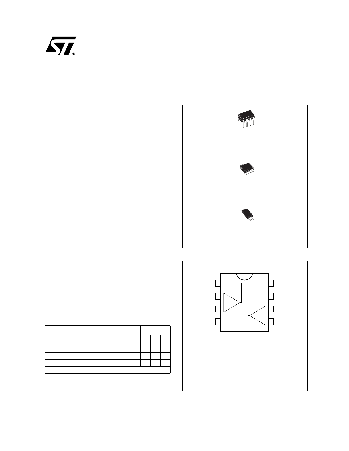
N
DIP8
(Plastic Package)
D
SO8
(Plastic Micropackage)
TSSOP8
(Thin Shrink Small Outline Package)
PIN CONNECTIONS (top view)
P
ORDER CODE
Part Number Temperature Range
TS27L2C/AC/BC 0°C, +70°C
TS27L2I/AI/BI -40°C, +125°C
TS27L2M/AM/BM -55°C, +125°C
Example : TS27L2ACN
N = Dual in Line Package (DIP)
D = Small Outline Package (SO) - also available in Tape & Reel (DT)
P = Thin Shrink Small Outline Package (TSSOP) - only available
in Tape & Reel (PT)
November 2001
Package
NDP
•••
•••
•••
1/9
TS27L2C,I,M
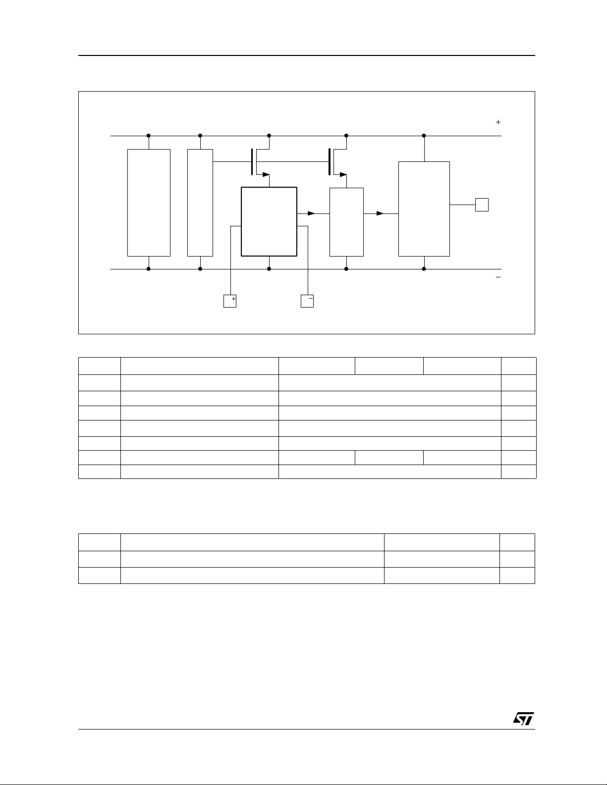
E
E
Input
differential
Second
stage
Output
stage
Output
CC
V
CC
V
Current
source
x I
BLOCK DIAGRAM
ABSOLUTE MAXIMUM RATINGS
Symbol Parameter TS27L2C/AC/BC TS27L2I/AI/BI TS27L2M/AM/BM Unit
+
V
T
T
1. All values, except differential voltage are with respect to network ground terminal.
2. Dif ferential voltages are the non-inv erting input terminal with respec t to t he i nverting i nput terminal .
3. The magnitud e of the input an d the output voltages must never excee d the magnit ude of the posi tive suppl y v ol tage.
Supply Voltage
CC
V
id Differential Input Voltage
V
Input Voltage
i
I
Output Current for V
o
I
Input Current ±5 mA
in
Operating Free-Air Temperature Range 0 to +70 -40 to +125 -55 to +125 °C
oper
Storage Temperature Range -65 to +150 °C
stg
1)
2)
3)
+
≥ 15V
CC
18 V
±18 V
-0.3 to 18 V
±30 mA
OPERATING CONDITIONS
Symbol Parameter Value Unit
+
V
V
Supply Voltage 3 to 16 V
CC
Common Mode Input Voltage Range
icm
0 to V
CC
+
- 1.5
V
2/9
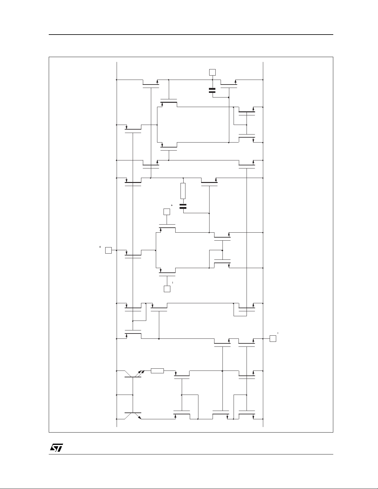
SCHEMATIC DIAGRAM (for 1/2 TS27L2)
TS27L2C,I,M
15
T
12
T
10
T
11
T
8
T
6
T
Output
7
T
16
T
14
T
13
T
9
T
R1
C1
Input
2
T
5
CC
V
T
1
T
4
T
3
T
27
T
26
T
25
T
24
T
Input
28
T
23
T
2
R
T
17 18
T
19
T
29
T
22
T
21
T
20
T
CC
V
3/9
 Loading...