

查询TS271AC供应商
.
OFFSET NULL CAPABILITY (by external
compensation)
.
DYNAMIC CHARACTERISTICS
ADJUSTABLEBY I
.
CONSUMPTION CURRENT AND DYNAMIC
PARAMETERS ARE STABLE REGARDING
THE VOLTAGEPOWER SUPPLY
VARIATIONS
.
OUTPUT VOLTAGE CAN SWING TO
GROUND
.
VERYLARGE I
.
STABLEAND LOW OFFSETVOLTAGE
.
THREE INPUT OFFSETVOLTAGE
SELECTIONS
SET
SET
RANGE
TS271C,I,M
PROGRAMMABLE CMOS
SINGLE OPERATIONAL AMPLIFIERS
N
DIP8
(Plastic Package)
(Plastic Micropackage)
D
SO8
DESCRIPTION
The TS271is a low cost, lowpowersingle operational amplifierdesigned to operate with single or
dual supplies. This operational amplifier uses the
SGS-THOMSONsilicon gate CMOS process giving it an excellent consumption-speedratio. This
amplifier is ideallysuited for low consumption
applications.
The powersupply is externallyprogrammablewith
a resistorconnectedbetweenpins8and4.Itallows
to choose the best consumption-speedratio and
supply current can be minimizedaccording to the
required speed. This device is specified for the
followingI
This CMOS amplifieroffers very high input impedance and extremelylow input currents.The major
advantage versus JFET devices is the very low
input currents drift withtemperature(see figure 3).
currentvalues: 1.5µA, 25µA,130µA.
SET
ORDER CODES
Part Number
TS271C/AC/BC 0
TS271I/AI/BI -40oC, +125oC ●●
TS271M/AM/BM -55oC, +125oC ●●
Example : TS271ACN
PIN CONNECTIONS (top view)
1
2
3
45
Temperature
Range
o
C, +70oC ●●
-
+
1 - Offset Null 1
2 - InvertingInput
3 - Non-invertingInput
-
4-V
CC
5 - Offset Null 2
6 - Output
7-V
+
CC
8-I
SET
Package
ND
8
7
6
October 1997
1/15
TS271C,I,M
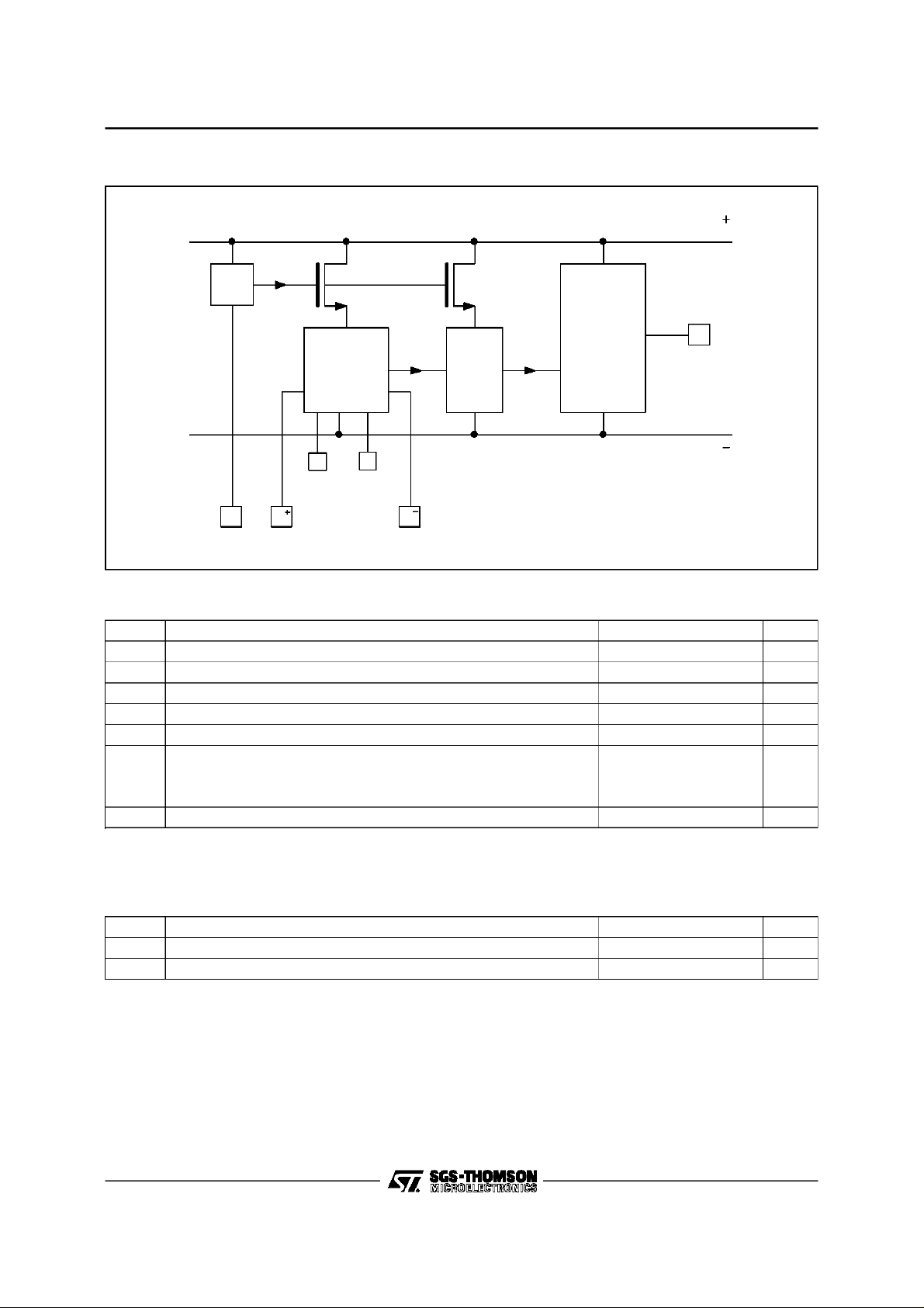
BLOCK DIAGRAM
Iset Input Input
Input
differential
Offset null
E E
Second
stage
Output
stage
V
CC
Output
V
CC
MAXIMUMRATINGS
Symbol Parameter Value Unit
+
V
T
T
Notes : 1. All voltage values, except differential voltage, are with respect to network ground terminal.
Supply Voltage - (note 1) 18 V
CC
Differential Input Voltage- (note 2) ±18 V
V
id
Input Voltage - (note 3) -0.3 to 18 V
V
i
Output Current for V
I
O
Input Current ±5mA
I
in
Operating Free-Air TemperatureRange
oper
Storage TemperatureRange -65 to +150
stg
2. Differential voltages are thenon-inverting input terminal with respect to the invertinginput terminal.
3. The magnitude of the input and the output voltages must never exceed the magnitude of the positive supply voltage.
+
≥ 15V ±30 mA
CC
TS271C/AC/BC
TS271I/AI/BI
TS271M/AM/BM
0to+70
-40 to +125
-55 to +125
OPERATINGCONDITIONS
Symbol Parameter Value Unit
+
V
V
Supply Voltage 3 to 16 V
CC
Common Mode Input Voltage Range 0 to V
icm
CC
+
- 1.5 V
o
C
o
C
2/15
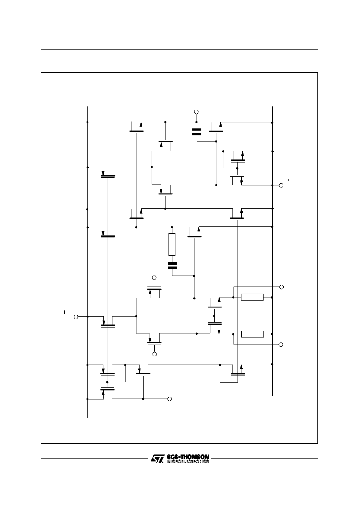
SCHEMATIC DIAGRAM
TS271C,I,M
T10
T6T5
T15
T8
R1
T12
T11
Output
C2
C1
T7
T16
T14
T13
T9
CC
V
T2 Input +
CC
V
Offset Null 2
T1
T3 T4
T27
T28
T26
Input -
Set Current
T29
Offset Null 1
3/15
TS271C,I,M
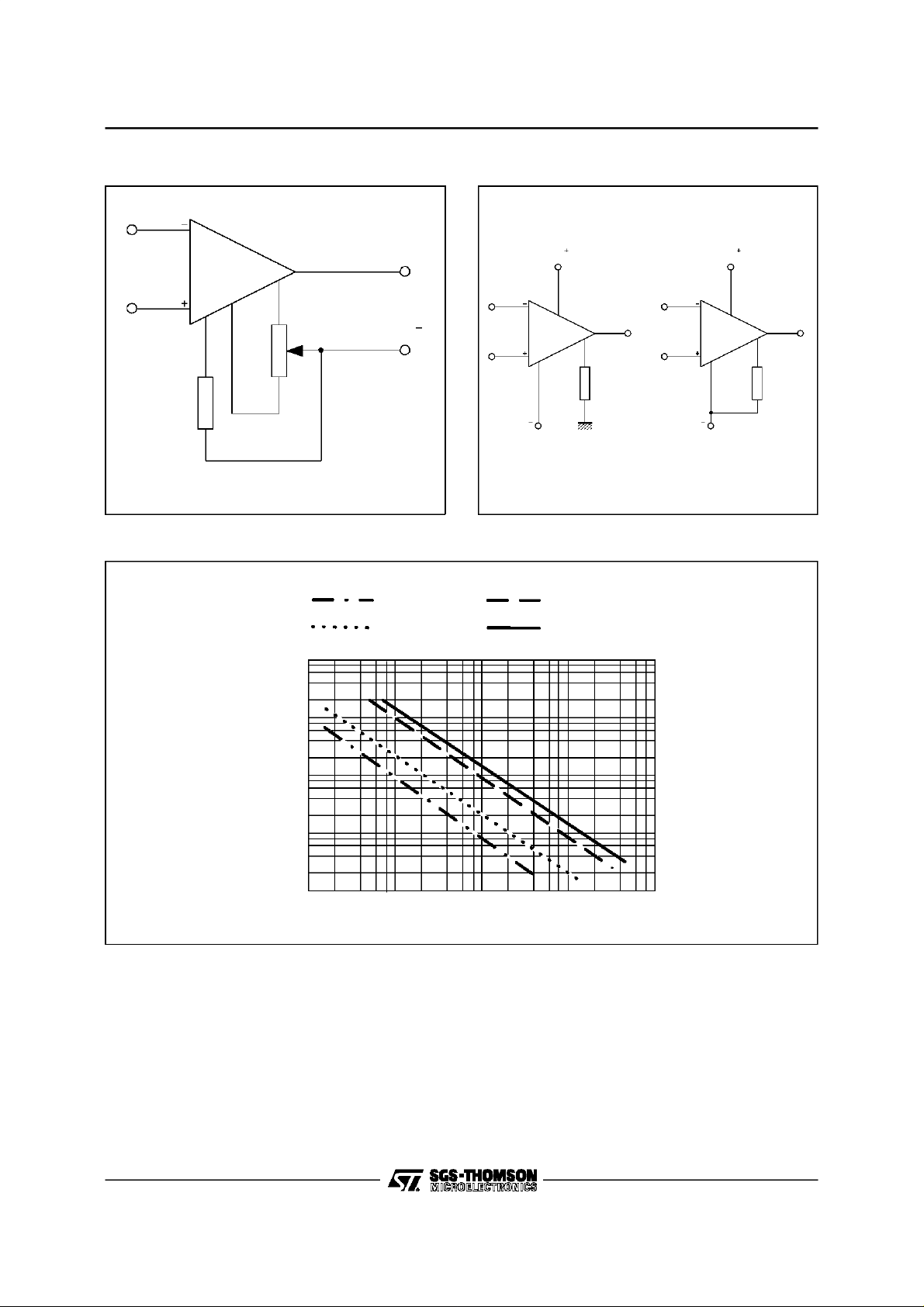
OFFSET VOLTAGENULL CIRCUIT
5
1
8
Ω
25k
R
set
OFFSETCOMPENSATION GUARANTEED FOR
TS271BCX (I
Figure 1 : R
>25µA),TS271ACX (I
SET
Connectedto V
SET
R
set
CC
SET
-
.
V
CC
>90µA)
V
CC
V
CC
= +3V
= +5V
RESISTOR BIASING
V
CC
R
set
V
CC
R
CONNECTED TO
SET
GROUND
V
= +10V
CC
= +16V
V
CC
V
CC
V
O
V
CC
CONNECTED TO
R
SET
-
(R
V
CC
Fig.1)
VALUE : SEE
SET
V
O
R
set
10M Ω
1M Ω
100k Ω
10k Ω
0.1µA
1
µA 10µA 100µA
I
set
4/15
TS271C,I,M
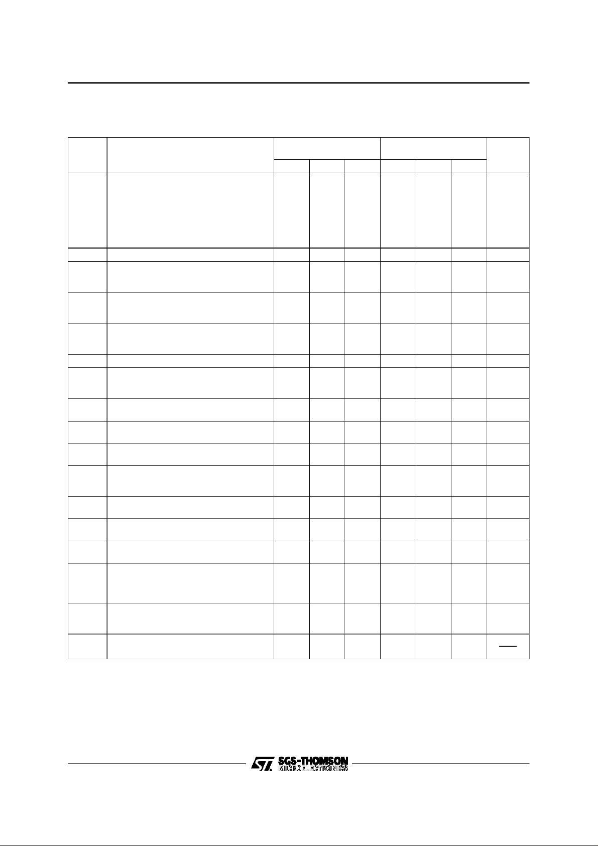
ELECTRICAL CHARACTERISTICS FOR I
+
V
= +10V,V
CC
Symbol Parameter
CC
-
=0V, T
=25oC (unless otherwisespecified)
amb
SET
= 1.5µA
TS271C/AC/BC
Min. Typ. Max. Min. Typ. Max.
V
Input Offset Voltage
io
= 1.4V,Vic= 0V TS271C/I/M
V
O
TS271AC/AI/AM
TS271BC/BI/BM
≤ T
T
min.
amb
≤ T
TS271C/I/M
max.
TS271AC/AI/AM
1.1
0.9
0.25
TS271BC/BI/BM
DV
V
V
A
GBP Gain Bandwidth Product (A
Input Offset VoltageDrift 0.7 0.7 µV/oC
io
Input Offset Current - (note 1)
I
io
I
ib
OH
OL
vd
=5V,Vo=5V
V
ic
. ≤ T
T
min
amb
≤ T
max
.
Input Bias Current - (note 1)
=5V,Vo=5V
V
ic
. ≤ T
T
min
amb
≤ T
max
.
High Level Output Voltage
= 100mV,RL=1MΩ
V
id
. ≤ T
T
min
amb
≤ T
max
.
8.8
8.7
Low Level Output Voltage (Vid= -100mV) 50 50 mV
Large Signal VoltageGain
=1Vto6V,RL=1MΩ,Vic=5V
V
o
. ≤ T
T
min
=1MΩ,CL= 100pF,fin= 10kHz) 0.1 0.1
R
L
amb
≤ T
max
.
= 40dB,
v
30
20
1
1
9 8.8
100 30
CMR Common Mode Rejection Ratio
V
= 1.4V,Vic= 1V to 7.4V 60 80 60 80
o
SVR Supply Voltage Rejection Ratio
I
CC
I
o
I
sink
+
V
= 5V to 10V ,Vo= 1.4V 60 80 60 80
CC
Supply Current
= 1, no load, Vo=5V
A
v
T
min
. ≤ T
amb
≤ T
max.
10 15
Output Short Circuit Current
= 100mV, Vo=0V 60 60
V
id
Output Sink Current
= -100mV, Vo=V
V
id
CC
45 45
SR Slew-Rate at Unity Gain
R
=1MΩ,CL= 100pF, Vi= 3 to7V 0.04 0.04
L
∅m Phase Margin at Unity Gain
A
= 40dB, RL=1MΩ
v
K
Note : 1. Maximum values including unavoidable inaccuracies of theindustrial test.
Overshoot Factor
ov
Equivalent Input Noise Voltage
e
n
f = 1kHz, R
= 100Ω 68 68
S
= 10pF
C
L
= 100pF
C
L
= 10pF
C
L
= 100pF
C
L
35
10
40
70
10
5
2
12
6.5
3
100
150
17
TS271I/AI/BI
TS271M/AM/BM
1.1
0.9
0.25
1
1
9
8.6
100
20
10 15
35
10
40
70
Unit
mV
10
5
2
12
6.5
3.5
pA
200
pA
300
V
V/mV
MHz
dB
dB
µA
18
mA
mA
V/µs
Degrees
%
nV
√Hz
5/15
 Loading...