

ST TS2431 User Manual
Programmable shunt voltage reference
Features
■ Adjustable output voltage: 2.5 to 24 V
■ Precision selection at 25 °C: ± 2%, ± 1% and
±0.5%
■ Sink current capability: 1 to 100 mA
■ Industrial temperature range: - 40 to +105 °C
■ Performances compatible with industry-
standard TL431
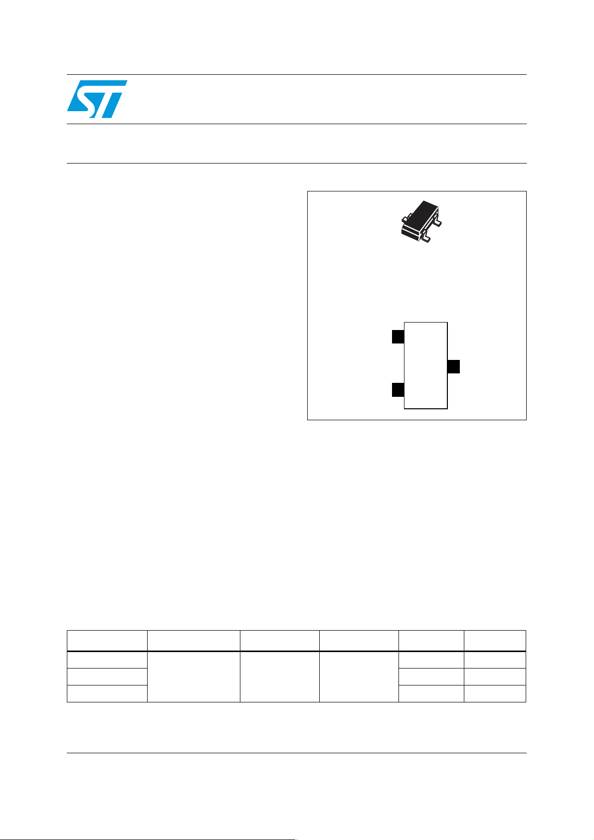
TS2431
Datasheet − production data
SOT23-3L
(plastic micropackage)
Pin connections (top view)
Applications
■ Computers
■ Instrumentation
■ Battery chargers
■ Switch mode power supplies
■ Battery-operated equipment
Description
The TS2431 is a programmable shunt voltage
reference with guaranteed temperature stability
over the entire temperature range of operation
- 40 to + 105 °C. The output voltage may be set to
any value between 2.5 and 24 V with an external
resistor bridge. Available in a SOT23-3L surface
mount package, the device can be implemented
in applications where space-saving is of utmost
importance.
Cathode
Reference
1
Anode
3
TS2431
2
Table 1. Device summary
Order codes Temperature range Package Packing Precision Marking
TS2431ILT
TS2431AILT 1% L286
TS2431BILT 0.5% L287
May 2012 Doc ID 7961 Rev 3 1/11
This is information on a product in full production.
-40 to +105°C SOT23-3L Tape and reel
2% L285
www.st.com
11

Contents TS2431
Contents
1 Absolute maximum ratings and operating conditions . . . . . . . . . . . . . 3
2 Electrical characteristics . . . . . . . . . . . . . . . . . . . . . . . . . . . . . . . . . . . . . 4
3 Package information . . . . . . . . . . . . . . . . . . . . . . . . . . . . . . . . . . . . . . . . . 8
3.1 SOT23-3L package information . . . . . . . . . . . . . . . . . . . . . . . . . . . . . . . . . 9
4 Revision history . . . . . . . . . . . . . . . . . . . . . . . . . . . . . . . . . . . . . . . . . . . 10
2/11 Doc ID 7961 Rev 3
TS2431 Absolute maximum ratings and operating conditions
1 Absolute maximum ratings and operating conditions
Table 2. Absolute maximum ratings
Symbol Parameter Value Unit
Vka Cathode to anode voltage 25 V
I
K
I
REF
P
T
std
ESD
T
LEAD
1. Pd has been calculated with Tamb = 25°C, Tjunction = 150°C, Rthjc = 110°C/W and Rthja = 340°C/W for
the SOT23-3 package.
2. Human body model: a 100 pF capacitor is charged to the specified voltage, then discharged through a
1.5 kΩ resistor between two pins of the device. This is done for all couples of connected pin combinations
while the other pins are floating.
3. Machine model: a 200 pF capacitor is charged to the specified voltage, then discharged directly between
two pins of the device with no external series resistor (internal resistor < 5 Ω). This is done for all couples of
connected pin combinations while the other pins are floating.
Table 3. Operating conditions
Reverse breakdown current -100 to +150 mA
Reference input current range -0.05 to +10 mA
Power dissipation
d
(1)
SOT23-3L
360 mW
Storage temperature -65 to +150 °C
(3)
(2)
2kV
200 V
Human body model (HBM)
Machine model (MM)
Lead temperature (soldering, 10 seconds) 260 °C
Symbol Parameter Value Unit
V
KA
I
K
T
oper
1. Maximum power dissipation must be strictly observed to avoid damaging the component.
Cathode to anode voltage V
Cathode operating current
(1)
to 24 V
REF
1 to 100 mA
Operating free air temperature range - 40 to + 105 °C
Doc ID 7961 Rev 3 3/11

Electrical characteristics TS2431
2 Electrical characteristics
Table 4. Electrical characteristics (Tamb = 25 °C unless otherwise specified)
Symbol Parameter Test condition Min. Typ. Max. Unit
V
= V
K
, IK = 10 mA 2.5
REF
TS2431 (2%) 2.45 2.55
V
Reference input voltage
REF
TS2431A (1%) 2.475 2.525
TS2431B (0.5%) 2.488 2.512
0 °C < T < +70 °C 10 20
-40 °C < T < +105 °C 20 35
-40 °C < T < +105 °C 50 100 ppm/°C
|ΔV
Reference input voltage deviation over
|
temperature
T
REF
C
= V
V
K
, IK = 10 mA
REF
Temperature coefficient
(1) (2)
(2)
T = 25 °C 0.3 0.8
I
KMIN
ΔVref
------------ --- -
ΔVk
I
|ΔI
I
|Z
Minimum operating current
Ratio of change in reference input
voltage to change in cathode to anode
voltage
Reference input current
REF
REF
OFF
KA
= 10 mA, R1 = 10 kΩ, R2 = +
I
K
Reference input current deviation
|
= 10 mA, R1 = 10 kΩ, R2 = +
I
K
Off-state cathode current VK = 24 V, V
| Reverse dynamic impedance
(3)
∞
(3)
∞
-40 °C < T < +105 °C 1
= 10 mA
I
K
Vka = 24 to 2.5 V
0.3 2 mV/V
T = 25 °C 0.5 2.5
-40 °C < T < +105 °C 3
-40 °C < T < +105 °C 0.4 1.2 µA
= GND 10 500 nA
REF
V
= V
K
REF
ΔIK = 1 to 50 mA,
0.5 0.75 W
f < 10 kHz
= 10 mA
I
E
N
Wide band noise
K
10 Hz < f < 10 kHz
300 nV/√Hz
V
mV-40 °C < T < +85 °C 17 30
mA
µA
1. Limits are 100% production tested at 25° C. Limits over temperature are guaranteed through correlation and by design.
|ΔV
2.
3. Refer to
| is defined as the difference between the maximum and minimum values of V
REF
range.
Figure 4: Test circuit for Vka = Vref on page 5
.
obtained over the full temperature
REF
4/11 Doc ID 7961 Rev 3
 Loading...