

1.8 V input/output, rail-to-rail, low power operational amplifiers
TS1871ILT
TS1874ID/IDT-TS1874IPT
TS1871ID/IDT
TS1872ID/IDT-TS1872IST-TS1872IPT
1
2
3
5
4
V
CC-
V
CC+
In-
Out
In+
V
CC-
1
2
3
5
4
8
7
6
N.C.
N.C.
In+
In-
Out
+
_
N.C.
V
CC+
In2+
V
CC-
1
2
3
5
4
8
7
6
In1+
In1-
Out2
+
_
Out1
In2-
+
_
V
CC+
In2+
V
CC-
1
2
3
5
4
8
7
6
In1+
In1-
Out2
+
_
Out1
In2-
+
_
V
CC+
V
CC-
1
2
3
11
4
14
13
12
In2+
In2-
Out4
Out2
In4+
In4-
5
6
7
8
10
9
+
_
+
_
+
_
Out3
In3+
In3-
+
_
Out1
In1+
In1-
V
CC+
V
CC-
1
2
3
11
4
14
13
12
In2+
In2-
Out4
Out2
In4+
In4-
5
6
7
8
10
9
+
_
+
_
+
_
Out3
In3+
In3-
+
_
Out1
In1+
In1-
V
CC+
Features
TS187x, TS187xA
Datasheet — production data
■ Operating range from V
CC
■ Rail-to-rail input and output
■ Extended V
icm
(V
CC-
- 0.2 V to V
■ Low supply current (400 µA)
■ Gain bandwidth product (1.6 MHz)
■ High unity gain stability
■ ESD tolerance (2 kV)
■ Latch-up immunity
■ Available in SOT23-5 micropackage
Applications
■ Battery-powered applications (toys)
■ Portable communication devices (cell phones)
■ Audio drivers (headphone drivers)
■ Laptop/notebook computers
Description
The TS187x (single, dual and quad) can operate
with voltages as low as 1.8 V. They feature both
input and output rail-to-rail.
The common-mode input voltage extends 200 mV
beyond the supply voltages at 25°C, while the
output voltage swing is within 100 mV of each rail
with a 600 Ω load resistor. The devices consume
typically 400 µA per channel while offering
1.6 MHz of gain bandwidth product. The
amplifiers provide a high output drive capability at
typically 65 mA loads.
= 1.8 to 6 V
CC+
+ 0.2 V)
These features make the TS187x family ideal for
sensor interface, battery supplied and portable
applications.
July 2012 Doc ID 6992 Rev 6 1/25
This is information on a product in full production.
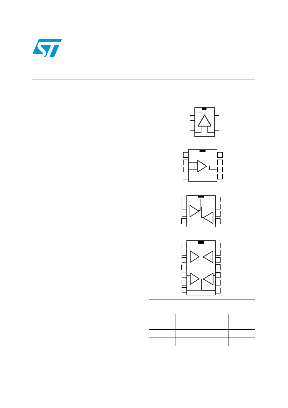
Table 1. Device summary
Reference
Single
version
TS187x TS1871 TS1872 TS1874
TS187xA TS1871A TS1872A TS1874A
Dual
version
Quad
version
www.st.com
25

Contents TS187x, TS187xA
Contents
1 Absolute maximum ratings and operating conditions . . . . . . . . . . . . . 3
2 Electrical characteristics . . . . . . . . . . . . . . . . . . . . . . . . . . . . . . . . . . . . . 5
3 Package information . . . . . . . . . . . . . . . . . . . . . . . . . . . . . . . . . . . . . . . . 16
3.1 SO-8 package information . . . . . . . . . . . . . . . . . . . . . . . . . . . . . . . . . . . . 17
3.2 TSSOP8 package information . . . . . . . . . . . . . . . . . . . . . . . . . . . . . . . . . 18
3.3 MiniSO-8 package information . . . . . . . . . . . . . . . . . . . . . . . . . . . . . . . . . 19
3.4 SO-14 package information . . . . . . . . . . . . . . . . . . . . . . . . . . . . . . . . . . . 20
3.5 TSSOP14 package information . . . . . . . . . . . . . . . . . . . . . . . . . . . . . . . . 21
3.6 SOT23-5 package information . . . . . . . . . . . . . . . . . . . . . . . . . . . . . . . . . 22
4 Ordering information . . . . . . . . . . . . . . . . . . . . . . . . . . . . . . . . . . . . . . . 23
5 Revision history . . . . . . . . . . . . . . . . . . . . . . . . . . . . . . . . . . . . . . . . . . . 24
2/25 Doc ID 6992 Rev 6
TS187x, TS187xA Absolute maximum ratings and operating conditions
1 Absolute maximum ratings and operating conditions
Table 2. Absolute maximum ratings
Symbol Parameter Value Unit
V
CC
V
id
V
in
T
stg
T
R
thja
R
thjc
ESD
Supply voltage
Differential input voltage
Input voltage V
Storage temperature -65 to +150 °C
Maximum junction temperature 150 °C
j
Thermal resistance junction to ambient
SOT23-5
MiniSO-8
SO-8
SO-14
TSSOP8
TSSOP14
Thermal resistance junction to case
SOT23-5
MiniSO-8
SO-8
SO-14
TSSOP8
TSSOP14
HBM: human body model
MM: machine model
CDM: charged device model
(1)
(5)
(2)
(4)
(6)
(3)
CC-
7V
±1 V
-0.3 to V
+0.3 V
CC+
250
190
125
°C/W
103
120
100
81
39
40
°C/W
31
37
32
2kV
200 V
1.5 kV
Latch-up immunity 200 mA
Lead temperature (soldering, 10 sec) 250 °C
Output short-circuit duration see note
1. All voltage values, except differential voltages, are with respect to network terminal.
2. Differential voltages are the non-inverting input terminal with respect to the inverting input terminal. If
> ±1 V, the maximum input current must not exceed ±1 mA. When Vid > ±1 V, add an input series
V
id
resistor to limit the input current.
3. Short-circuits can cause excessive heating. Destructive dissipation can result from simultaneous short-
circuits on all amplifiers.
4. Human body model: a 100 pF capacitor is charged to the specified voltage, then discharged through a
5. Machine model: a 200 pF capacitor is charged to the specified voltage, then discharged directly between
6. Charged device model: all pins and package are charged together to the specified voltage and then
7. Short-circuits from the output to V
Ω resistor between two pins of the device. This is done for all couples of connected pin combinations
1.5 k
while the other pins are floating.
two pins of the device with no external series resistor (internal resistor < 5
connected pin combinations while the other pins are floating.
discharged directly to ground through only one pin. This is done for all pins.
can cause excessive heating. The maximum output current is
approximately 80 mA, independent of the magnitude of V
simultaneous short-circuits on all amplifiers.
CC
. Destructive dissipation can result from
CC
Ω). This is done for all couples of
(7)
Doc ID 6992 Rev 6 3/25
Absolute maximum ratings and operating conditions TS187x, TS187xA
Table 3. Operating conditions
Symbol Parameter Value Unit
V
V
T
CC
icm
oper
Supply voltage 1.8 to 6 V
Common-mode input voltage range
T
= 25°C, 1.8 ≤ V
oper
T
< T
min
oper
< T
max
≤ 6V
CC
, 1.8 ≤ V
CC
≤ 6V
- 0.2 to V
CC-
V
CC-
to V
CC+
CC+
+ 0.2
V
V
Operating free-air temperature range -40 to + 125 °C
4/25 Doc ID 6992 Rev 6
TS187x, TS187xA Electrical characteristics
2 Electrical characteristics
Table 4. Electrical characteristics measured at V
V
CC
/2, and T
= +1.8 V with V
= 25°C (unless otherwise specified)
amb
CC+
(1)
= 0 V, CL and RL connected to
CC-
Symbol Parameter Conditions Min. Typ. Max. Unit
= V
= VCC/2
out
≤ T
≤ T
≤ T
= V
≤ T
= V
≤ T
icm
≤ T
amb
amb
amb
amb
≤ V
amb
≤ T
= VCC/2
out
≤ T
= VCC/2
out
≤ T
CC, Vout
≤ T
max
max
max
max
max
= 0.5 to 1.3 V
≤ T
≤ T
≤ T
≤ T
≤ T
amb
amb
amb
amb
≤ T
≤ T
≤ T
max, RL
max, RL
max, RL
max, RL
= VCC/2
= 1, no load
≤ T
≤ T
amb
max
(2)
(2)
= VCC/2
= 2 kΩ
= 600 Ω
= 2 kΩ
= 600 Ω
CC-
CC+
555277
777091
1.65
1.62
1.65
1.62
20 58
20 68
1
1.5
0.1
3
6
330
60
40 125
150
84
1.77
1.74
3046100
150
100
150
400 560
600
V
Input offset voltage
io
ΔV
CMR
V
V
Input offset voltage drift 2 µV/°C
io
I
Input offset current
io
I
Input bias current
ib
Common mode rejection ratio
20 log (ΔV
Large signal voltage gain
A
vd
High level output voltage
OH
Low level output voltage
OL
/ΔVio)
ic
Output source current Vid = 100 mV, VO = V
I
o
Output sink current V
I
Supply current (per amplifier)
CC
GBP Gain bandwidth product R
V
icm
TS1871A/2A/4A
T
min
TS1871/2/4
T
min
V
icm
T
min
V
icm
T
min
0 ≤ V
T
min
V
out
RL = 2 kΩ
= 600 Ω
R
L
V
= 100 mV
id
R
= 2 kΩ
L
R
= 600 Ω
L
T
min
T
min
= -100 mV
V
id
RL = 2 kΩ
= 600 Ω
R
L
T
min
T
min
= -100 mV, VO = V
id
V
out
A
VCL
T
min
= 10 kΩ, CL = 100 pF, f = 100 kHz 0.9 1.6 MHz
L
SR Slew rate RL = 10 kΩ, CL = 100 pF, AV = 1 0.38 0.54 V/µs
mV
nA
nA
dB
dB
V
mV
mA
µA
φmPhase margin C
e
Input voltage noise f = 1 kHz 27 nV/√Hz
n
= 100 pF 53 Degrees
L
THD Total harmonic distortion 0.01 %
1. All parameter limits at temperatures different from 25°C are guaranteed by correlation.
2. Maximum values include unavoidable inaccuracies of the industrial tests.
Doc ID 6992 Rev 6 5/25
Electrical characteristics TS187x, TS187xA
Table 5. Electrical characteristics measured at VCC = +3 V with VDD = 0 V, CL and RL connected to
V
CC
/2, and T
= 25°C (unless otherwise specified)
amb
(1)
Symbol Parameter Conditions Min. Typ. Max. Unit
V
= V
icm
TS1871A/2A/4A
V
Input offset voltage
io
T
min
TS1871/2/4
T
min
ΔV
CMR
Input offset voltage drift 2 µV/°C
io
V
I
Input offset current
io
I
Input bias current
ib
Common mode rejection ratio
20 log (ΔV
Large signal voltage gain
A
vd
/ΔVio)
ic
icm
T
min
V
icm
T
min
0 ≤ V
T
min
V
out
R
L
R
L
V
id
RL = 2 kΩ
V
V
High level output voltage
OH
Low level output voltage
OL
R
L
T
min
T
min
V
id
R
L
R
L
T
min
T
min
Output source current Vid = 100 mV, VO = V
I
o
Output sink current V
I
Supply current (per amplifier)
CC
GBP Gain bandwidth product R
SR Slew rate R
φmPhase margin C
e
Input voltage noise f = 1 kHz 27 nV/√Hz
n
V
A
T
id
out
VCL
min
L
L
L
= 2 kΩ
= 600 Ω
= 600 Ω
= -100 mV
= 2 kΩ
= 600 Ω
= -100 mV, VO = V
= 10 kΩ, CL = 100 pF, f = 100 kHz 1 1.7 MHz
= 10 kΩ, CL = 100 pF, AV = 1 0.42 0.6 V/µs
= 100 pF 53 Degrees
= VCC/2
out
≤ T
≤ T
amb
≤ T
≤ T
amb
= V
= VCC/2
out
≤ T
≤ T
amb
= V
= VCC/2
out
≤ T
≤ T
amb
≤ V
icm
CC, Vout
≤ T
≤ T
amb
= 0.5 to 2.5 V
= 100 mV
≤ T
≤ T
amb
≤ T
≤ T
amb
≤ T
≤ T
amb
≤ T
≤ T
amb
= VCC/2
= 1, no load
≤ T
≤ T
amb
max
max
(2)
max
(2)
max
= VCC/2
max
, RL = 2 kΩ
max
max, RL
max, RL
max, RL
CC-
max
= 600 Ω
= 2 kΩ
= 600 Ω
CC+
60
57
807494
2.82
2.80
2.82
2.80
20 60
20 70
1
1.5
0.1
3
6
330
60
4125
150
80 dB
88
2.95
2.95
3958120
160
120
160
450 650
690
mV
nA
nA
dB
mV
mA
µA
THD Total harmonic distortion 0.01 %
V
1. All parameter limits at temperatures different from 25°C are guaranteed by correlation.
2. Maximum values include unavoidable inaccuracies of the industrial tests.
6/25 Doc ID 6992 Rev 6
TS187x, TS187xA Electrical characteristics
Table 6. Electrical characteristics measured at VCC = +5 V with VDD = 0 V, CL and RL connected to
V
CC
/2, and T
= 25°C (unless otherwise specified)
amb
(1)
Symbol Parameter Conditions Min. Typ. Max. Unit
V
= V
icm
TS1871A/2A/4A
V
Input offset voltage
io
T
min
TS1871/2/4
T
min
ΔV
CMR
SVR
Input offset voltage drift 2 µV/°C
io
V
I
Input offset current
io
I
Input bias current
ib
Common mode rejection ratio
20 log (ΔV
/ΔVio)
ic
Supply voltage rejection ratio
20 log (ΔV
A
Large signal voltage gain
vd
cc
/ΔVio)
icm
T
min
V
icm
T
min
0 ≤ V
T
min
VCC = 1.8 to 5 V 70 90 dB
V
out
R
L
R
L
V
id
RL = 2 kΩ
V
V
High level output voltage
OH
Low level output voltage
OL
R
L
T
min
T
min
V
id
R
L
R
L
T
min
T
min
Output source current Vid = 100 mV, VO = V
I
o
Output sink current Vid = -100 mV, VO = V
V
out
I
Supply current (per amplifier)
CC
GBP Gain bandwidth product R
SR Slew rate R
φmPhase margin C
e
Input voltage noise f = 1 kHz 27 nV/√Hz
n
A
T
VCL
min
L
L
L
= 2 kΩ
= 600 Ω
= 100 mV
= 600 Ω
= -100 mV
= 2 kΩ
= 600 Ω
= 10 kΩ, CL = 100 pF, f = 100 kHz 1 1.8 MHz
= 10 kΩ, CL = 100 pF, AV = 1 0.42 0.6 V/µs
= 100 pF 55 Degrees
= VCC/2
out
≤ T
≤ T
amb
≤ T
≤ T
amb
= V
= VCC/2
out
≤ T
≤ T
amb
= V
= VCC/2
out
≤ T
≤ T
amb
≤ V
icm
CC, Vout
≤ T
≤ T
amb
= 1 to 4 V
≤ T
≤ T
amb
≤ T
≤ T
amb
≤ T
≤ T
amb
≤ T
≤ T
amb
= VCC/2
= 1, no load
≤ T
≤ T
amb
max
max
(2)
max
(2)
max
not equal to VCC/2
max
= 2 kΩ
max, RL
, RL = 600 Ω
max
= 2 kΩ
max, RL
= 600 Ω
max, RL
CC-
CC+
max
656285
837797
4.80
4.75
4.80
4.75
20 65
20 80
1
1.5
0.1
3
6
330
60
70 130
150
91
4.95
4.90
5270130
188
130
188
500 835
875
mV
nA
nA
dB
dB
mV
mA
µA
THD Total harmonic distortion 0.01 %
V
1. All parameter limits at temperatures different from 25°C are guaranteed by correlation.
2. Maximum values include unavoidable inaccuracies of the industrial tests.
Doc ID 6992 Rev 6 7/25
Electrical characteristics TS187x, TS187xA
-2. -1.6 -1.2 -.8 -.4 0 .4 .8 1.2 1.6 2
Input offset voltage (mV)
0
20
40
60
80
100
120
140
160
492 pieces tested
Vcc = 5V
Temp = +25°C
Quantity of pieces
-2. -1.6 -1.2 -.8 -.4 0 .4 .8 1.2 1.6 2
Input offset voltage (mV)
0
20
40
60
80
100
120
140
160
492 pieces tested
Vcc = 5V
Temp = +25°C
492 pieces tested
Vcc = 5V
Temp = +25°C
Quantity of pieces
-40 -20 0 20 40 60 80 100 120 140
Temperature (°C)
-150
-100
-50
0
50
100
150
200
Input Off set voltage (µV)
Vcc = 3V
Vcc = 1.8V
Vcc = 5V
-40 -20 0 20 40 60 80 100 120 140
Temperature (°C)
-150
-100
-50
0
50
100
150
200
Input Off set voltage (µV)
Vcc = 3V
Vcc = 1.8V
Vcc = 5V
-40 -20 0 20 40 60 80 100 120 140
Temperature (°C)
-40.0
-30.0
-20.0
-10.0
0.0
10.0
Input bias current (nA)
Vcc = 1.8V
Vicm = 0.9V
-40 -20 0 20 40 60 80 100 120 140
Temperature (°C)
-40.0
-30.0
-20.0
-10.0
0.0
10.0
Input bias current (nA)
Vcc = 1.8V
Vicm = 0.9V
-40 -20 0 20 40 60 80 100 120 140
Temperature (°C)
-40.0
-30.0
-20.0
-10.0
0.0
10.0
Input bi as cu rrent (nA)
Vcc = 3V
Vicm = 1.5V
-40 -20 0 20 40 60 80 100 120 140
Temperature (°C)
-40.0
-30.0
-20.0
-10.0
0.0
10.0
Input bi as cu rrent (nA)
Vcc = 3V
Vicm = 1.5V
02468
Supply voltage (V)
0
100
200
300
400
500
600
Supply current (µA)
Tamb = 25°C
02468
Supply voltage (V)
0
100
200
300
400
500
600
Supply current (µA)
Tamb = 25°C
-40 -20 0 20 40 60 80 100 120 140
Temperature (°C)
250
300
350
400
450
500
550
Supply current (µA)
Vcc = 5V
Vcc = 3V
Vcc = 1.8V
-40 -20 0 20 40 60 80 100 120 140
Temperature (°C)
250
300
350
400
450
500
550
Supply current (µA)
Vcc = 5V
Vcc = 3V
Vcc = 1.8V
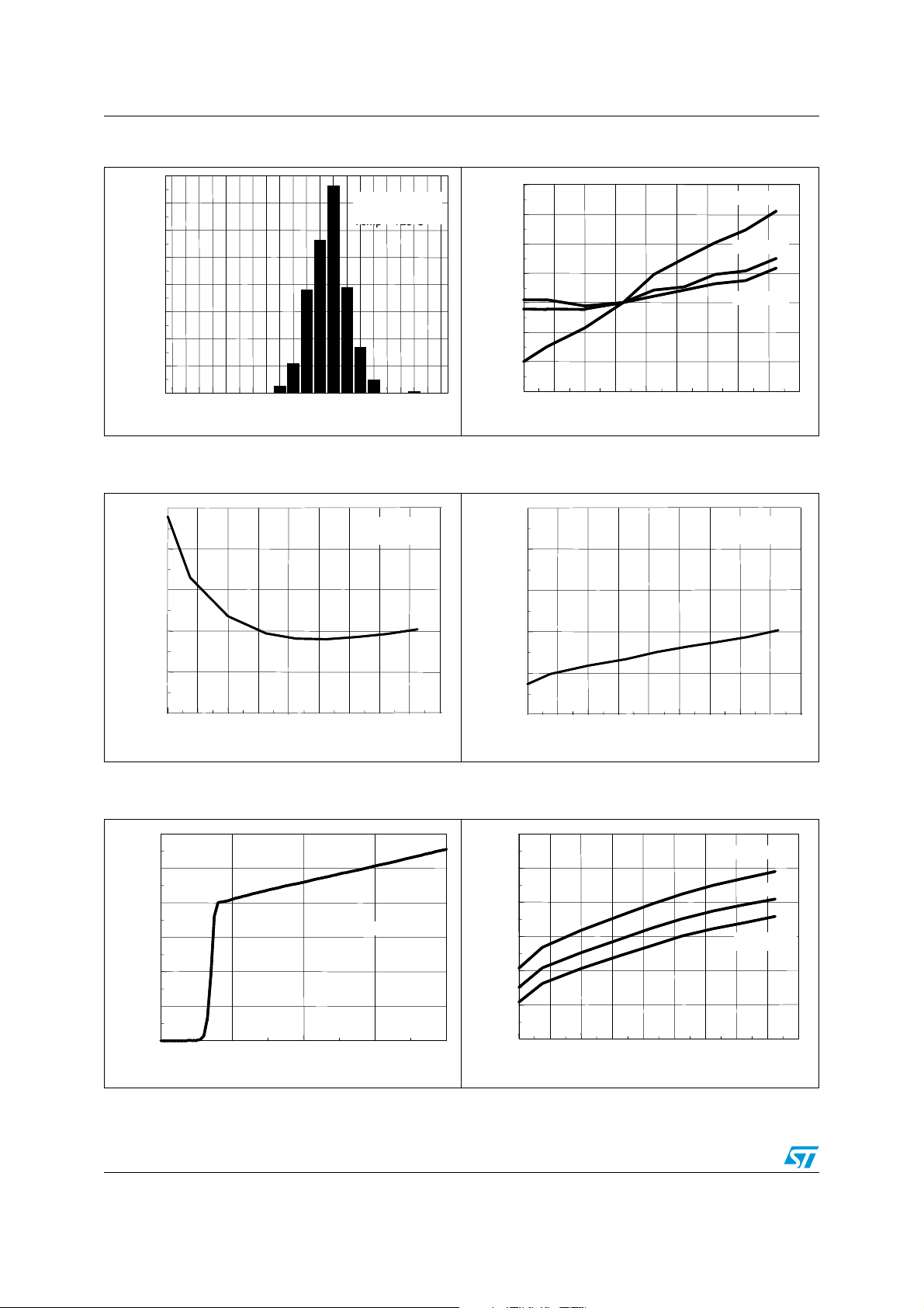
Figure 1. Input offset voltage distribution Figure 2. Input offset voltage vs. temperature
Figure 3. Input bias current vs. temperature
at Vcc = 1.8 V
Figure 4. Input bias current vs. temperature
at Vcc = 3 V
Figure 5. Supply current/amplifier vs. supply
Figure 6. Supply current/amplifier vs.
voltage
8/25 Doc ID 6992 Rev 6
temperature

TS187x, TS187xA Electrical characteristics
-40 -20 0 20 40 60 80 100 120 140
Temperature (°C)
85
90
95
100
105
110
115
120
Common mode rejection (dB)
Vcc = 1.8V
Vicm = 0V
Vcc = 3V
Vicm = 0V
Vcc = 5V
Vicm = 0V
-40 -20 0 20 40 60 80 100 120 140
Temperature (°C)
85
90
95
100
105
110
115
120
Common mode rejection (dB)
Vcc = 1.8V
Vicm = 0V
Vcc = 3V
Vicm = 0V
Vcc = 5V
Vicm = 0V
-40 -20 0 20 40 60 80 100 120 140
Temperature (°C)
60
70
80
90
100
110
Supply voltage rejection (dB)
Vcc = 1.8V
Vicm = 0V
-40 -20 0 20 40 60 80 100 120 140
Temperature (°C)
60
70
80
90
100
110
Supply voltage rejection (dB)
Vcc = 1.8V
Vicm = 0V
-40 -20 0 20 40 60 80 100 120 140
Temperature (°C)
60
70
80
90
100
110
Supply voltage rejection (dB)
Vcc = 3V
Vicm = 0V
-40 -20 0 20 40 60 80 100 120 140
Temperature (°C)
60
70
80
90
100
110
Supply voltage rejection (dB)
Vcc = 3V
Vicm = 0V
-40 -20 0 20 40 60 80 100 120 140
Temperature (°C)
60
70
80
90
100
110
Supply voltage rejection (dB)
Vcc = 5V
Vicm = 0V
-40 -20 0 20 40 60 80 100 120 140
Temperature (°C)
60
70
80
90
100
110
Supply voltage rejection (dB)
Vcc = 5V
Vicm = 0V
100 1000 10000 100000
Frequency (Hz)
-80
-70
-60
-50
-40
-30
-20
Supply voltage rejection (d B)
Vcc = 1.8V
Vicm = 0.7V
Gain = 10
100 1000 10000 100000
Frequency (Hz)
-80
-70
-60
-50
-40
-30
-20
Supply voltage rejection (d B)
Vcc = 1.8V
Vicm = 0.7V
Gain = 10
-40 -20 0 20 40 60 80 100 120 140
Temperature (°C)
70
80
90
100
110
Open loop gain (dB)
Vcc = 1.8V
Vicm = 0.9V
RL = 600 Ohms
RL = 2 kOhms
-40 -20 0 20 40 60 80 100 120 140
Temperature (°C)
70
80
90
100
110
Open loop gain (dB)
Vcc = 1.8V
Vicm = 0.9V
RL = 600 Ohms
RL = 2 kOhms
Figure 7. Common mode rejection vs.
temperature
Figure 9. Supply voltage rejection vs.
temperature at Vcc = 3 V
Figure 8. Supply voltage rejection vs.
temperature at Vcc = 1.8 V
Figure 10. Supply voltage rejection vs.
temperature at Vcc = 5 V
Figure 11. Power supply voltage rejection vs.
frequency
Doc ID 6992 Rev 6 9/25
Figure 12. Open loop gain vs. temperature
at Vcc = 1.8 V

Electrical characteristics TS187x, TS187xA
-40 -20 0 20 40 60 80 100 120 140
Temperature (°C)
70
80
90
100
110
Open loop gain (dB)
Vcc = 3V
Vicm = 1.5V
RL = 600 Ohms
RL = 2 kOhms
-40 -20 0 20 40 60 80 100 120 140
Temperature (°C)
70
80
90
100
110
Open loop gain (dB)
Vcc = 3V
Vicm = 1.5V
RL = 600 Ohms
RL = 2 kOhms
-40 -20 0 20 40 60 80 100 120 140
Temperature (°C)
70
80
90
100
110
Open loop gain (dB)
Vcc = 5V
Vicm = 2.5V
RL = 600 ohms
RL = 2 kOhms
-40 -20 0 20 40 60 80 100 120 140
Temperature (°C)
70
80
90
100
110
Open loop gain (dB)
Vcc = 5V
Vicm = 2.5V
RL = 600 ohms
RL = 2 kOhms
-40 -20 0 20 40 60 80 100 120 140
Temperature (°C)
40
50
60
70
80
90
100
110
Voltage referenced to VCC (mV)
Vcc = 1.8V
Vcc = 3V
Vcc = 5V
RL = 600 ohms
-40 -20 0 20 40 60 80 100 120 140
Temperature (°C)
40
50
60
70
80
90
100
110
Voltage referenced to VCC (mV)
Vcc = 1.8V
Vcc = 3V
Vcc = 5V
RL = 600 ohms
-40 -20 0 20 40 60 80 100 120 140
Temperature (°C)
40
50
60
70
80
90
100
110
Voltage referenced to Gnd (mV)
Vcc = 1.8V
Vcc = 3V
Vcc = 5V
RL = 600 ohms
-40 -20 0 20 40 60 80 100 120 140
Temperature (°C)
40
50
60
70
80
90
100
110
Voltage referenced to Gnd (mV)
Vcc = 1.8V
Vcc = 3V
Vcc = 5V
RL = 600 ohms
-40 -20 0 20 40 60 80 100 120 140
Temperature (°C)
20
30
40
50
60
70
80
Voltage referenced to VCC (mV)
Vcc = 1.8V
Vcc = 3V
Vcc = 5V
RL = 2 kohms
-40 -20 0 20 40 60 80 100 120 140
Temperature (°C)
20
30
40
50
60
70
80
Voltage referenced to VCC (mV)
Vcc = 1.8V
Vcc = 3V
Vcc = 5V
RL = 2 kohms
-40 -20 0 20 40 60 80 100 120 140
Temperature (°C)
20
30
40
50
60
70
80
Voltage referenced to VCC (mV)
Vcc = 1.8V
Vcc = 3V
Vcc = 5V
RL = 2 kohms
-40 -20 0 20 40 60 80 100 120 140
Temperature (°C)
20
30
40
50
60
70
80
Voltage referenced to VCC (mV)
Vcc = 1.8V
Vcc = 3V
Vcc = 5V
RL = 2 kohms
Figure 13. Open loop gain vs. temperature
at Vcc = 3 V
Figure 15. High level output voltage vs.
temperature, R
= 600 Ω
L
Figure 14. Open loop gain vs. temperature
at Vcc = 5 V
Figure 16. Low level output voltage vs.
temperature, RL = 600 Ω
Figure 17. High level output voltage vs.
temperature, R
10/25 Doc ID 6992 Rev 6
= 2 kΩ
L
Figure 18. Low level output voltage vs.
temperature, RL = 2 kΩ

TS187x, TS187xA Electrical characteristics
-40 -20 0 20 40 60 80 100 120 140
Temperature (°C)
-100
-50
0
50
100
Output current (mA)
Isink
Vcc = 1.8V
Vid = 1V
Isource
-40 -20 0 20 40 60 80 100 120 140
Temperature (°C)
-100
-50
0
50
100
Output current (mA)
Isink
Vcc = 1.8V
Vid = 1V
Isource
-40 -20 0 20 40 60 80 100 120 140
Temperature (°C)
-100
-50
0
50
100
Output current (mA)
Isink
Vcc = 3V
Vid = 1V
Isource
-40 -20 0 20 40 60 80 100 120 140
Temperature (°C)
-100
-50
0
50
100
Output current (mA)
Isink
Vcc = 3V
Vid = 1V
Isource
-40 -20 0 20 40 60 80 100 120 140
Temperature (°C)
-100
-50
0
50
100
Output current (mA)
Isink
Vcc = 5V
Vid = 1V
Isource
-40 -20 0 20 40 60 80 100 120 140
Temperature (°C)
-100
-50
0
50
100
Output current (mA)
Isink
Vcc = 5V
Vid = 1V
Isource
0.0 0.5 1.0 1.5 2.0
Output volt age (V)
-100
-50
0
50
100
Output current (mA)
sink
Vcc = 1.8V
Vid = 0.1V
Vicm = 0.9V
source
T = 25 °C
T = -40 °C
T = 125 °C
T = 125 °C
T = -40 °C
T = 25 °C
0.0 0.5 1.0 1.5 2.0
Output volt age (V)
-100
-50
0
50
100
Output current (mA)
sink
Vcc = 1.8V
Vid = 0.1V
Vicm = 0.9V
source
T = 25 °C
T = -40 °C
T = 125 °C
T = 125 °C
T = -40 °C
T = 25 °C
0.0 0.5 1.0 1.5 2.0 2.5 3.0 3.5
Output volt age (V)
-100
-50
0
50
100
Output current (mA)
sink
Vcc = 3V
Vid = 0.1V
Vicm = 1.5V
source
T = 25 °C
T = -40 °C
T = 125 °C
T = 125 °C
T = -40 °C
T = 25 °C
0.0 0.5 1.0 1.5 2.0 2.5 3.0 3.5
Output volt age (V)
-100
-50
0
50
100
Output current (mA)
sink
Vcc = 3V
Vid = 0.1V
Vicm = 1.5V
source
T = 25 °C
T = -40 °C
T = 125 °C
T = 125 °C
T = -40 °C
T = 25 °C
0.0 1.0 2.0 3.0 4.0 5.0
Output volt age (V)
-100
-50
0
50
100
Output current (mA)
sink
Vcc = 5V
Vid = 0. 1V
Vicm = 2.5V
source
T = 25 °C
T = -40 °C
T = 125 °C
T = 125 °C
T = -40 °C
T = 25 °C
0.0 1.0 2.0 3.0 4.0 5.0
Output volt age (V)
-100
-50
0
50
100
Output current (mA)
sink
Vcc = 5V
Vid = 0. 1V
Vicm = 2.5V
source
T = 25 °C
T = -40 °C
T = 125 °C
T = 125 °C
T = -40 °C
T = 25 °C
Figure 19. Output current vs. temperature
at Vcc = 1.8 V
Figure 21. Output current vs. temperature
at Vcc = 5 V
Figure 20. Output current vs. temperature
at Vcc = 3 V
Figure 22. Output current vs. output voltage
at Vcc = 1.8 V
Figure 23. Output current vs. output voltage
at Vcc = 3 V
Figure 24. Output current vs. output voltage
at Vcc = 5 V
Doc ID 6992 Rev 6 11/25

Electrical characteristics TS187x, TS187xA
1E+3 1E+4 1E+5 1E+6
Frequency (Hz)
0
10
20
30
40
50
60
70
Gain (dB)
40
60
80
100
120
140
160
180
Phase (°)
RL = 10K
CL = 100 pF
Vcc = 1.8V
gain
phase
1E+3 1E+4 1E+5 1E+6
Frequency (Hz)
0
10
20
30
40
50
60
70
Gain (dB)
40
60
80
100
120
140
160
180
Phase (°)
RL = 10K
CL = 100 pF
Vcc = 1.8V
gain
phase
1E+3 1E+4 1E+5 1E+6
Frequency (Hz)
0
10
20
30
40
50
60
70
Gain (dB)
40
60
80
100
120
140
160
180
Phase (°)
RL = 10K
CL = 100 pF
Vcc = 3V
gain
phase
1E+3 1E+4 1E+5 1E+6
Frequency (Hz)
0
10
20
30
40
50
60
70
Gain (dB)
40
60
80
100
120
140
160
180
Phase (°)
RL = 10K
CL = 100 pF
Vcc = 3V
gain
phase
1E+3 1E+4 1E+5 1E+6
Frequency (Hz)
0
10
20
30
40
50
60
70
Gain (dB)
40
60
80
100
120
140
160
180
Phase (°)
RL = 10K
CL = 100 pF
Vcc = 5V
gain
phase
1E+3 1E+4 1E+5 1E+6
Frequency (Hz)
0
10
20
30
40
50
60
70
Gain (dB)
40
60
80
100
120
140
160
180
Phase (°)
RL = 10K
CL = 100 pF
Vcc = 5V
gain
phase
-40 -20 0 20 40 60 80 100 120 140
Temperature (°C)
1.20
1.30
1.40
1.50
1.60
1.70
Gain-bandwidth product (MHz)
Vcc = 1.8V
Vcc = 3V
Vcc = 5V
Vicm = Vcc/2
RL = 10kohms
CL = 100 pF
-40 -20 0 20 40 60 80 100 120 140
Temperature (°C)
1.20
1.30
1.40
1.50
1.60
1.70
Gain-bandwidth product (MHz)
Vcc = 1.8V
Vcc = 3V
Vcc = 5V
Vicm = Vcc/2
RL = 10kohms
CL = 100 pF
12345
Supply voltage (V)
0.5
1.0
1.5
2.0
Gain bandwidth product (MHz)
RL = 2 kohms
CL = 220 pF
Vicm = Vcc/2
T = 25°C
12345
Supply voltage (V)
0.5
1.0
1.5
2.0
Gain bandwidth product (MHz)
RL = 2 kohms
CL = 220 pF
Vicm = Vcc/2
T = 25°C
-40 -20 0 20 40 60 80 100 120 140
Temperature (°C)
0.30
0.35
0.40
0.45
0.50
0.55
Slew rate (V/µs)
positive slew rate
Vcc = 1.8V
gain = +1
Vin = 0.4 to 1.4V
RL = 10kohm
CL = 100 pF
negative slew rate
-40 -20 0 20 40 60 80 100 120 140
Temperature (°C)
0.30
0.35
0.40
0.45
0.50
0.55
Slew rate (V/µs)
positive slew rate
Vcc = 1.8V
gain = +1
Vin = 0.4 to 1.4V
RL = 10kohm
CL = 100 pF
negative slew rate
Figure 25. Gain and phase vs. frequency
at Vcc = 1.8 V
Figure 27. Gain and phase vs. frequency
at Vcc = 5 V
Figure 26. Gain and phase vs. frequency
at Vcc = 3 V
Figure 28. Gain bandwidth product vs.
temperature
Figure 29. Gain bandwidth product vs. supply
voltage
12/25 Doc ID 6992 Rev 6
Figure 30. Slew rate vs. temperature at
Vcc = 1.8 V

TS187x, TS187xA Electrical characteristics
-40 -20 0 20 40 60 80 100 120 140
Temperature (°C)
0.35
0.40
0.45
0.50
0.55
0.60
0.65
0.70
Slew rate (V/µs)
positive slew rate
Vcc = 3V
gain = +1
Vin = 1 to 2V
RL = 10kohm
CL = 100 pF
negative slew rate
-40 -20 0 20 40 60 80 100 120 140
Temperature (°C)
0.35
0.40
0.45
0.50
0.55
0.60
0.65
0.70
Slew rate (V/µs)
positive slew rate
Vcc = 3V
gain = +1
Vin = 1 to 2V
RL = 10kohm
CL = 100 pF
negative slew rate
-40 -20 0 20 40 60 80 100 120 140
Temperature (°C)
0.35
0.40
0.45
0.50
0.55
0.60
0.65
0.70
0.75
Slew rate (V/µs)
positiv e slew rate
Vcc = 5V
gain = +1
Vin = 2 to 3V
RL = 10kohms
CL = 100 pF
negative slew rate
-40 -20 0 20 40 60 80 100 120 140
Temperature (°C)
0.35
0.40
0.45
0.50
0.55
0.60
0.65
0.70
0.75
Slew rate (V/µs)
positiv e slew rate
Vcc = 5V
gain = +1
Vin = 2 to 3V
RL = 10kohms
CL = 100 pF
negative slew rate
10 100 1000
Load capacitor (pF)
-10
0
10
20
30
40
50
60
Phase margin (°)
Vcc = 1.8V
gain = 40dB
RL = 1Kohm
10 100 1000
Load capacitor (pF)
-10
0
10
20
30
40
50
60
Phase margin (°)
Vcc = 1.8V
gain = 40dB
RL = 1Kohm
-10 -5 0 5 10
DC output current (mA)
40
45
50
55
60
65
70
75
80
Phase margin (°)
Vcc = 1.8V
RL = 1 kOhm
CL = 220 pF
-10 -5 0 5 10
DC output current (mA)
40
45
50
55
60
65
70
75
80
Phase margin (°)
Vcc = 1.8V
RL = 1 kOhm
CL = 220 pF
-10 -5 0 5 10
DC output current (mA)
-25
-20
-15
-10
-5
0
GainmMargin (dB)
Vcc = 1.8V
RL = 1 kOhm
CL = 220 pF
-10 -5 0 5 10
DC output current (mA)
-25
-20
-15
-10
-5
0
GainmMargin (dB)
Vcc = 1.8V
RL = 1 kOhm
CL = 220 pF
1E+1 1E+2 1E+3 1E+4 1E+5
Frequency (Hz)
5
10
15
20
25
30
35
Equivalent input noise (nV/sqrt(Hz))
Vcc = 1.8V
gain = 100
Rs = 100 ohms
1E+1 1E+2 1E+3 1E+4 1E+5
Frequency (Hz)
5
10
15
20
25
30
35
Equivalent input noise (nV/sqrt(Hz))
Vcc = 1.8V
gain = 100
Rs = 100 ohms
Figure 31. Slew rate vs. temperature at
Vcc = 3 V
Figure 32. Slew rate vs. temperature at
Vcc = 5 V
Figure 33. Phase margin vs. load capacitor Figure 34. Phase margin vs. output current
Figure 35. Gain margin vs. output current Figure 36. Equivalent input noise vs.
frequency
Doc ID 6992 Rev 6 13/25

Electrical characteristics TS187x, TS187xA
0.00 0.10 0.20 0.30 0.40 0.50 0.60 0.70 0080
Output voltage (VRMS)
0.001
0.010
0.100
1.000
10.000
100.000
Distortion (%)
RL= 1Kohms
Gain = -1
F = 1000 Hz
Vcc = 1.8V
0.00 0.10 0.20 0.30 0.40 0.50 0.60 0.70 0080
Output voltage (VRMS)
0.001
0.010
0.100
1.000
10.000
100.000
Distortion (%)
RL= 1Kohms
Gain = -1
F = 1000 Hz
Vcc = 1.8V
0.00 0.20 0.40 0.60 0.80 1.00 1.20
Output volt age (VRMS)
0.001
0.010
0.100
1.000
10.000
100.000
Distortion (%)
RL= 1Kohms
Gain = -1
F = 1000 Hz
Vcc = 3V
0.00 0.20 0.40 0.60 0.80 1.00 1.20
Output volt age (VRMS)
0.001
0.010
0.100
1.000
10.000
100.000
Distortion (%)
RL= 1Kohms
Gain = -1
F = 1000 Hz
Vcc = 3V
0.00 0.50 1.00 1.50 2.00
Output voltage (V RMS)
0.001
0.010
0.100
1.000
10.000
100.000
Distortion (%)
RL= 1Kohms
Gain = -1
F = 1000 Hz
Vcc = 5V
0.00 0.50 1.00 1.50 2.00
Output voltage (V RMS)
0.001
0.010
0.100
1.000
10.000
100.000
Distortion (%)
RL= 1Kohms
Gain = -1
F = 1000 Hz
Vcc = 5V
0.00 0.20 0.40 0.60 0.80 1.00 1.20
Output vol tage (VRMS )
0.001
0.010
0.100
1.000
10.000
100.000
Distortion (%)
RL= 150 ohms
Gain = -1
F = 1000 Hz
Vcc = 2.7V
0.00 0.20 0.40 0.60 0.80 1.00 1.20
Output vol tage (VRMS )
0.001
0.010
0.100
1.000
10.000
100.000
Distortion (%)
RL= 150 ohms
Gain = -1
F = 1000 Hz
Vcc = 2.7V
0.00 0.20 0.40 0.60 0.80 1.00 1.20
Output voltage (VRMS)
0.001
0.010
0.100
1.000
10.000
100.000
Distortion (%)
RL= 1500 ohms
Gain = -1
F = 1000 Hz
Vcc = 2.7V
0.00 0.20 0.40 0.60 0.80 1.00 1.20
Output voltage (VRMS)
0.001
0.010
0.100
1.000
10.000
100.000
Distortion (%)
RL= 1500 ohms
Gain = -1
F = 1000 Hz
Vcc = 2.7V
0.00 0.20 0.,40 0.60 0.80 1.00 1.20
Output voltage (VRMS)
0.001
0.010
0.100
1.000
10.000
100.000
Distortion (%)
RL= 4700 ohms
Gain = -1
F = 1000 Hz
Vcc = 2.7V
0.00 0.20 0.,40 0.60 0.80 1.00 1.20
Output voltage (VRMS)
0.001
0.010
0.100
1.000
10.000
100.000
Distortion (%)
RL= 4700 ohms
Gain = -1
F = 1000 Hz
Vcc = 2.7V
Figure 37. Distortion vs. output voltage at
Vcc = 1.8 V
Figure 39. Distortion vs. output voltage at
Vcc = 5 V
Figure 38. Distortion vs. output voltage at
Vcc = 3 V
Figure 40. Distortion vs. output voltage at
Vcc = 2.7 V, R
= 150 Ω
L
Figure 41. Distortion vs. output voltage at
Vcc = 2.7 V, R
14/25 Doc ID 6992 Rev 6
= 1500 Ω
L
Figure 42. Distortion vs. output voltage at
Vcc = 2.7 V, RL = 4700 Ω

TS187x, TS187xA Electrical characteristics
1E+1 1E+2 1E+3 1E+4 1E+5
Frequency (Hz)
0,004.
0.006
0.008
0.010
0.012
0.014
Distortion (%)
Vcc = 1.8V
Vout = 1Vpp
RL = 1Kohms
gain = -1
1E+1 1E+2 1E+3 1E+4 1E+5
Frequency (Hz)
0,004.
0.006
0.008
0.010
0.012
0.014
Distortion (%)
Vcc = 1.8V
Vout = 1Vpp
RL = 1Kohms
gain = -1
1E+1 1E+2 1E+3 1E+4 1E+5
Frequency (Hz)
0.000
0.003
0.005
0.007
0.010
0.013
0.015
Vcc = 3V
Vout = 1Vpp
RL = 1Kohms
gain = -1
Distortion (%)
1E+1 1E+2 1E+3 1E+4 1E+5
Frequency (Hz)
0.000
0.003
0.005
0.007
0.010
0.013
0.015
Vcc = 3V
Vout = 1Vpp
RL = 1Kohms
gain = -1
Distortion (%)
1E+1 1E+2 1E+3 1E+4 1E+5
Frequency (Hz)
0.000
0.025
0.050
0.075
0.100
0.125
0.150
Vcc = 1.8V
Vout = 1Vpp
RL = 32 ohms
gain = -1
Distortion (%)
1E+1 1E+2 1E+3 1E+4 1E+5
Frequency (Hz)
0.000
0.025
0.050
0.075
0.100
0.125
0.150
Vcc = 1.8V
Vout = 1Vpp
RL = 32 ohms
gain = -1
Distortion (%)
1E+1 1E+2 1E+3 1E+4 1E+5
Frequency (Hz)
0.000
0.025
0.050
0.075
0.100
0.125
0.150
Vcc = 3V
Vout = 1Vpp
RL = 32 ohms
gain = -1
Distortion (%)
1E+1 1E+2 1E+3 1E+4 1E+5
Frequency (Hz)
0.000
0.025
0.050
0.075
0.100
0.125
0.150
Vcc = 3V
Vout = 1Vpp
RL = 32 ohms
gain = -1
Distortion (%)
123456
Supply voltage (V)
0
10
20
30
40
50
60
Output power (mW)
10% distortion
1% distortion
0.1% distortion
RL = 32 ohms
123456
Supply voltage (V)
0
10
20
30
40
50
60
Output power (mW)
10% distortion
1% distortion
0.1% distortion
RL = 32 ohms
10
1
10
2
10
3
00
2020
4040
6060
8080
100100
CMRR (dB)
Figure 43. Distortion vs. frequency at
Vcc = 1.8 V
Figure 45. Distortion vs. frequency at
Vcc = 1.8 V, R
= 32 Ω
L
Figure 44. Distortion vs. frequency at
Vcc = 3 V
Figure 46. Distortion vs. frequency at
Vcc = 3 V, RL = 32 Ω
Figure 47. Output power vs. supply voltage Figure 48. Common mode rejection ratio vs.
frequency at Vcc = 5 V
Doc ID 6992 Rev 6 15/25

Package information TS187x, TS187xA
3 Package information
In order to meet environmental requirements, ST offers these devices in different grades of
ECOPACK
specifications, grade definitions and product status are available at: www.st.com.
ECOPACK
®
packages, depending on their level of environmental compliance. ECOPACK®
®
is an ST trademark.
16/25 Doc ID 6992 Rev 6
TS187x, TS187xA Package information
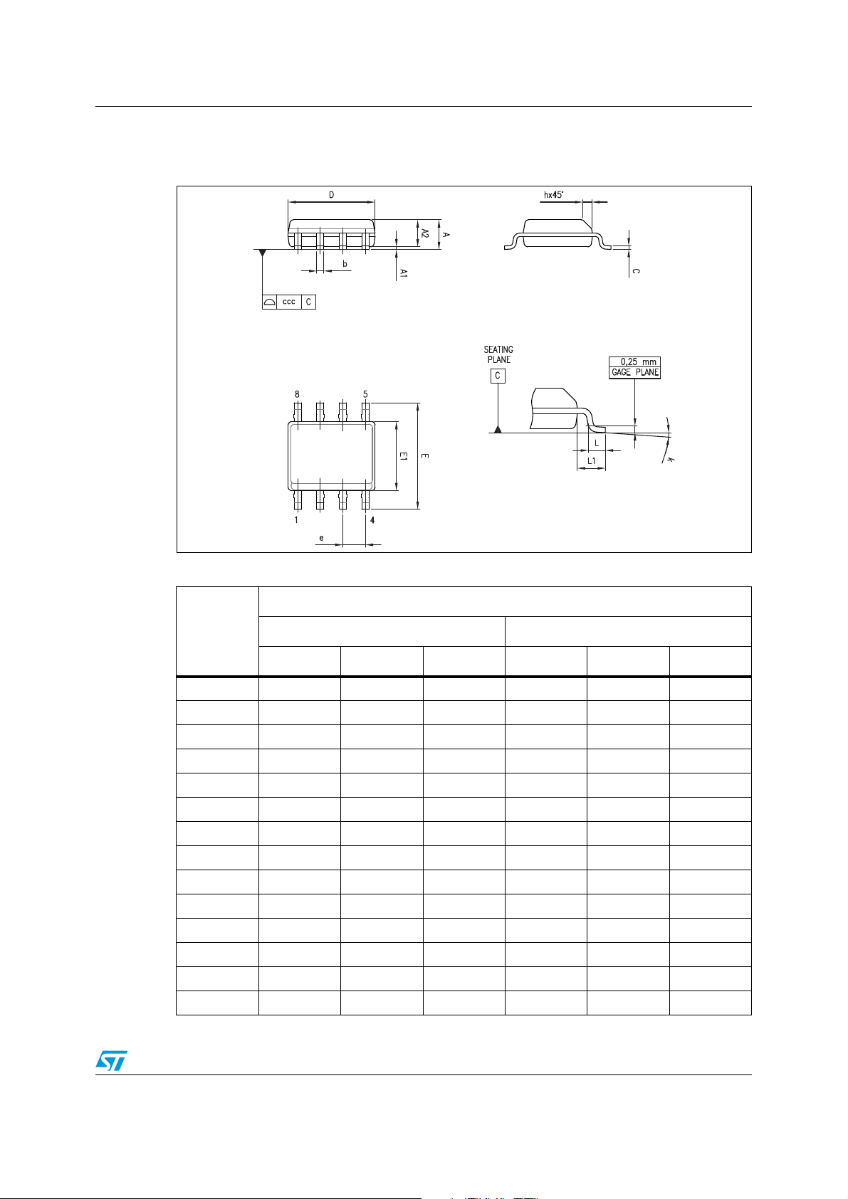
3.1 SO-8 package information
Figure 49. SO-8 package mechanical drawing
Table 7. SO-8 package mechanical data
Dimensions
Ref.
Min. Typ. Max. Min. Typ. Max.
A 1.75 0.069
A1 0.10 0.25 0.004 0.010
A2 1.25 0.049
b 0.28 0.48 0.011 0.019
c 0.17 0.23 0.007 0.010
D 4.80 4.90 5.00 0.189 0.193 0.197
E 5.80 6.00 6.20 0.228 0.236 0.244
E1 3.80 3.90 4.00 0.150 0.154 0.157
e 1.27 0.050
h 0.25 0.50 0.010 0.020
L 0.40 1.27 0.016 0.050
L1 1.04 0.040
k1°8°1°8°
ccc 0.10 0.004
Millimeters Inches
Doc ID 6992 Rev 6 17/25

Package information TS187x, TS187xA
3.2 TSSOP8 package information
Figure 50. TSSOP8 package mechanical drawing
Table 8. TSSOP8 package mechanical data
Dimensions
Ref.
Min. Typ. Max. Min. Typ. Max.
A 1.20 0.047
A1 0.05 0.15 0.002 0.006
A2 0.80 1.00 1.05 0.031 0.039 0.041
b 0.19 0.30 0.007 0.012
c 0.09 0.20 0.004 0.008
D 2.90 3.00 3.10 0.114 0.118 0.122
E 6.20 6.40 6.60 0.244 0.252 0.260
E1 4.30 4.40 4.50 0.169 0.173 0.177
e 0.65 0.0256
k0°8°0°8°
L 0.45 0.60 0.75 0.018 0.024 0.030
L1 1 0.039
aaa 0.10 0.004
Millimeters Inches
18/25 Doc ID 6992 Rev 6

TS187x, TS187xA Package information
3.3 MiniSO-8 package information
Figure 51. MiniSO-8 package mechanical drawing
Table 9. MiniSO-8 package mechanical data
Dimensions
Ref.
Min. Typ. Max. Min. Typ. Max.
A1.10.043
A1 0 0.15 0 0.006
A2 0.75 0.85 0.95 0.030 0.033 0.037
b 0.22 0.40 0.009 0.016
c 0.08 0.23 0.003 0.009
D 2.80 3.00 3.20 0.11 0.118 0.126
E 4.65 4.90 5.15 0.183 0.193 0.203
E1 2.80 3.00 3.10 0.11 0.118 0.122
e 0.65 0.026
L 0.40 0.60 0.80 0.016 0.024 0.031
L1 0.95 0.037
L2 0.25 0.010
k0°8°0°8°
Millimeters Inches
ccc 0.10 0.004
Doc ID 6992 Rev 6 19/25

Package information TS187x, TS187xA
3.4 SO-14 package information
Figure 52. SO-14 package mechanical drawing
Table 10. SO-14 package mechanical data
Dimensions
Millimeters Inches
Ref.
Min. Typ. Max. Min. Typ. Max.
A 1.35 1.75 0.05 0.068
A1 0.10 0.25 0.004 0.009
A2 1.10 1.65 0.04 0.06
B 0.33 0.51 0.01 0.02
C 0.19 0.25 0.007 0.009
D 8.55 8.75 0.33 0.34
E 3.80 4.0 0.15 0.15
e 1.27 0.05
H 5.80 6.20 0.22 0.24
h 0.25 0.50 0.009 0.02
L 0.40 1.27 0.015 0.05
k8° (max.)
ddd 0.10 0.004
20/25 Doc ID 6992 Rev 6
TS187x, TS187xA Package information
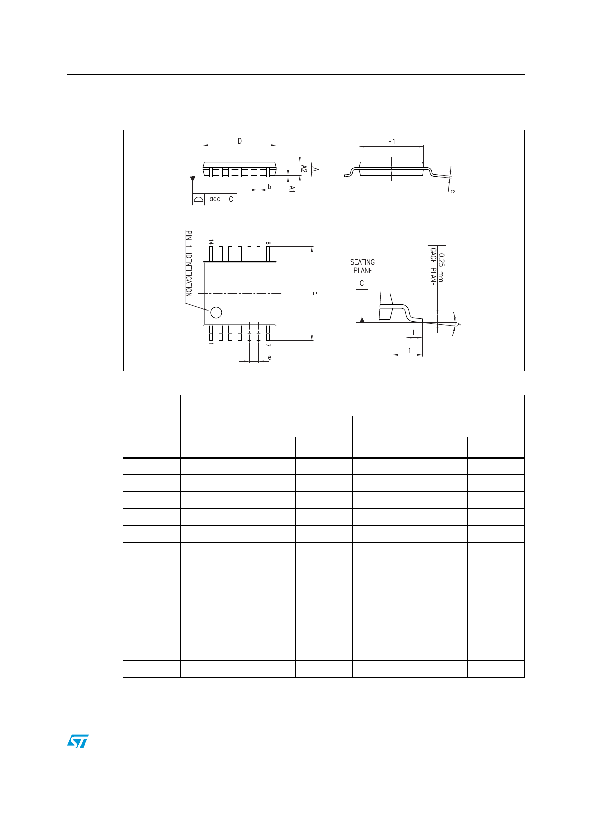
3.5 TSSOP14 package information
Figure 53. TSSOP14 package mechanical drawing
Table 11. TSSOP14 package mechanical data
Dimensions
Ref.
Min. Typ. Max. Min. Typ. Max.
A 1.20 0.047
A1 0.05 0.15 0.002 0.004 0.006
A2 0.80 1.00 1.05 0.031 0.039 0.041
b 0.19 0.30 0.007 0.012
c 0.09 0.20 0.004 0.0089
D 4.90 5.00 5.10 0.193 0.197 0.201
E 6.20 6.40 6.60 0.244 0.252 0.260
E1 4.30 4.40 4.50 0.169 0.173 0.176
e 0.65 0.0256
L 0.45 0.60 0.75 0.018 0.024 0.030
L1 1.00 0.039
k0°8°0°8°
aaa 0.10 0.004
Millimeters Inches
Doc ID 6992 Rev 6 21/25

Package information TS187x, TS187xA
3.6 SOT23-5 package information
Figure 54. SOT23-5L package mechanical drawing
Table 12. SOT23-5L package mechanical data
Dimensions
Ref.
Min. Typ. Max. Min. Typ. Max.
A 0.90 1.20 1.45 0.035 0.047 0.057
A1 0.15 0.006
A2 0.90 1.05 1.30 0.035 0.041 0.051
B 0.35 0.40 0.50 0.013 0.015 0.019
C 0.09 0.15 0.20 0.003 0.006 0.008
D 2.80 2.90 3.00 0.110 0.114 0.118
D1 1.90 0.075
e 0.95 0.037
E 2.60 2.80 3.00 0.102 0.110 0.118
F 1.50 1.60 1.75 0.059 0.063 0.069
L 0.10 0.35 0.60 0.004 0.013 0.023
K0° 10°
Millimeters Inches
22/25 Doc ID 6992 Rev 6

TS187x, TS187xA Ordering information
4 Ordering information
Table 13. Order codes
TS1871ID/IDT
TS1871IAID/AIDT 1871AI
TS1871ILT
Order code
Temperature
range
Package Packing Marking
SO-8
Tube or
tape & reel
1871I
K171
SOT23-5L Tape & reel
TS1871AILT K172
TS1871IYLT
TS1871AIYLT K183
TS1872ID/IDT
TS1872AID/AIDT 1872AI
TS1872IYDT
TS1872AIYDT 1872AY
SOT23-5L
(Automotive grade)
SO-8
SO-8
(Automotive grade)
Ta p e & re e l
Tube or
tape & reel
Tube or
tape & reel
TS1872IPT
K182
1872I
1872Y
1872I
TSSOP8 Tape & reel
TS1872AIPT 1872A
TS1872IYPT
TS1872AIYPT
(1)
(1)
-40°C to +125°C
TSSOP8
(Automotive grade)
Ta p e & re e l
1872Y
872AY
TS1872IST
K171
MiniSO-8 Tape & reel
TS1872AIST K172
TS1874ID/IDT
SO-14
TS1874AID/AIDT 1874AI
TS1874IYDT
TS1874AIYDT TS1874AY
SO-14
(Automotive grade)
Tube or
tape & reel
Tube or
tape & reel
TS1874IPT
1874I
TS1874Y
1874I
TSSOP14 Tape & reel
TS1874AIPT 1874AI
TS1874IYPT
TS1874AIYPT
1. Qualification and characterization according to AEC Q100 and Q003 or equivalent, advanced screening according to AEC
Q001 & Q 002 or equivalent are on-going.
(1)
(1)
TSSOP14
(Automotive grade)
Ta p e & re e l
TS1874Y
TS1874AY
Doc ID 6992 Rev 6 23/25

Revision history TS187x, TS187xA
5 Revision history
Table 14. Document revision history
Date Revision Changes
01-Apr-2002 1 First release.
02-Jan-2005 2
Modifications on AMR Table 2 on page 3 (explanation of V
V
limits).
i
id
and
Added limits over temperature range in Table 4 on page 5,
Table 5 on page 6, Table 6 on page 7.
Added SVR in Table 6 (SVR parameter removed from Table 4
and Ta bl e 5 ).
21-May-2007 3
Added equivalent input voltage noise in Ta bl e 4 , Ta bl e 5 , and
Ta b l e 6 .
Added R
values in Ta b l e 2 .
thjc
Added automotive grade part numbers to order codes table.
Moved order codes table to Section 4 on page 23.
Updated format of package information.
17-Jan-2008 4 Updated footnote for automotive grade order codes in Ta bl e 1 3.
Updated document format.
Modified headings, added root part number TS187xA and
added Table 1: Device summary on cover page.
Corrected typical values for A
, Isource, Isink and Vol in
Vd
Ta b l e 4 , Ta bl e 5 and Ta b le 6 .
12-Mar-2010 5
Added Figure 48: Common mode rejection ratio vs. frequency
at Vcc = 5 V.
Updated package information in Chapter 3.
Removed order codes for SO-8 automotive grade packages
(TS1871IYDT and TS1871AIYDT) from Ta bl e 1 3 .
Removed order codes for DIP package from Table 13.
06-Jul-2012 6 Updated Table 13: Order codes.
24/25 Doc ID 6992 Rev 6

TS187x, TS187xA
Please Read Carefully:
Information in this document is provided solely in connection with ST products. STMicroelectronics NV and its subsidiaries (“ST”) reserve the
right to make changes, corrections, modifications or improvements, to this document, and the products and services described herein at any
time, without notice.
All ST products are sold pursuant to ST’s terms and conditions of sale.
Purchasers are solely responsible for the choice, selection and use of the ST products and services described herein, and ST assumes no
liability whatsoever relating to the choice, selection or use of the ST products and services described herein.
No license, express or implied, by estoppel or otherwise, to any intellectual property rights is granted under this document. If any part of this
document refers to any third party products or services it shall not be deemed a license grant by ST for the use of such third party products
or services, or any intellectual property contained therein or considered as a warranty covering the use in any manner whatsoever of such
third party products or services or any intellectual property contained therein.
UNLESS OTHERWISE SET FORTH IN ST’S TERMS AND CONDITIONS OF SALE ST DISCLAIMS ANY EXPRESS OR IMPLIED
WARRANTY WITH RESPECT TO THE USE AND/OR SALE OF ST PRODUCTS INCLUDING WITHOUT LIMITATION IMPLIED
WARRANTIES OF MERCHANTABILITY, FITNESS FOR A PARTICULAR PURPOSE (AND THEIR EQUIVALENTS UNDER THE LAWS
OF ANY JURISDICTION), OR INFRINGEMENT OF ANY PATENT, COPYRIGHT OR OTHER INTELLECTUAL PROPERTY RIGHT.
UNLESS EXPRESSLY APPROVED IN WRITING BY TWO AUTHORIZED ST REPRESENTATIVES, ST PRODUCTS ARE NOT
RECOMMENDED, AUTHORIZED OR WARRANTED FOR USE IN MILITARY, AIR CRAFT, SPACE, LIFE SAVING, OR LIFE SUSTAINING
APPLICATIONS, NOR IN PRODUCTS OR SYSTEMS WHERE FAILURE OR MALFUNCTION MAY RESULT IN PERSONAL INJURY,
DEATH, OR SEVERE PROPERTY OR ENVIRONMENTAL DAMAGE. ST PRODUCTS WHICH ARE NOT SPECIFIED AS "AUTOMOTIVE
GRADE" MAY ONLY BE USED IN AUTOMOTIVE APPLICATIONS AT USER’S OWN RISK.
Resale of ST products with provisions different from the statements and/or technical features set forth in this document shall immediately void
any warranty granted by ST for the ST product or service described herein and shall not create or extend in any manner whatsoever, any
liability of ST.
ST and the ST logo are trademarks or registered trademarks of ST in various countries.
Information in this document supersedes and replaces all information previously supplied.
The ST logo is a registered trademark of STMicroelectronics. All other names are the property of their respective owners.
© 2012 STMicroelectronics - All rights reserved
STMicroelectronics group of companies
Australia - Belgium - Brazil - Canada - China - Czech Republic - Finland - France - Germany - Hong Kong - India - Israel - Italy - Japan -
Malaysia - Malta - Morocco - Philippines - Singapore - Spain - Sweden - Switzerland - United Kingdom - United States of America
www.st.com
Doc ID 6992 Rev 6 25/25
 Loading...