

TS185x, TS185xA
1.8 V input/output, rail-to-rail, low power operational amplifiers
Features
■ Operating range from V
■ Rail-to-rail input and output
■ Extended V
icm
(V
CC-
■ Low supply current (120 μA)
■ Good accuracy (1 mV max for A version)
■ Gain bandwidth product (530 kHz)
■ High unity gain stability (able to drive 500 pF)
■ ESD tolerance (2 kV)
■ Latch-up immunity
■ Available in SOT23-5 micropackage
= 1.8 to 6 V
CC
- 0.2 V to V
CC +
+ 0.2 V)
Applications
■ Two-cell battery-powered systems
■ Battery-powered electronic equipment
■ Cordless phones
■ Cellular phones
■ Laptops
■ PDAs
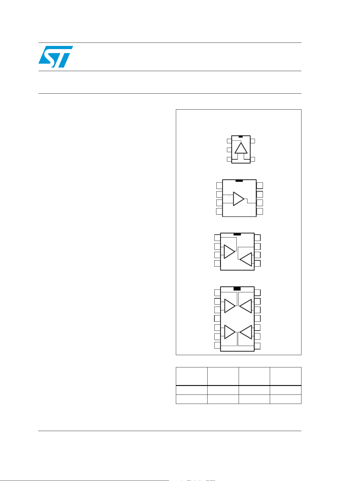
Pin connections (top view)
TS1851ILT
V
Out
CC-
In+
1
2
3
V
5
CC+
In-
4
TS1851ID/IDT
N.C.
In-
In+
V
CC-
1
_
2
+
3
4
N.C.
8
7
V
CC+
Out
6
N.C.
5
TS1852ID/IDT-TS1852IST-TS1852IPT
Out1
Out1
In1-
In1-
In1+
In1+
V
V
CC-
CC-
1
1
_
_
2
2
+
+
3
3
4
4
8
8
V
V
CC+
CC+
7
7
Out2
Out2
_
_
In2-
In2-
6
6
+
+
In2+
In2+
5
5
TS1854ID/IDT-TS1854IPT
Out4
Description
The TS185x (single, dual and quad) can operate
with voltages as low as 1.8 V. They feature both
input and output rail-to-rail (1.71 at V
R
=2kΩ), 120 μA current consumption and
L
530 kHz gain bandwidth product.
With this low consumption and a sufficient GBP
= 1.8 V,
CC
Out1
Out1
In1-
In1-
In1+
In1+
V
V
CC+
CC+
In2+
In2+
In2-
In2-
Out2
Out2
1
1
_
_
2
2
+
+
3
3
4
4
5
5
+
+
_
_
6
6
7
7
Out4
14
14
_
_
13
13
In4-
In4-
+
+
In4+
In4+
12
12
V
V
11
11
CC-
CC-
10
10
In3+
In3+
+
+
_
_
In3-
In3-
9
9
Out3
Out3
8
8
for many applications, these operational
amplifiers are well-suited to all kinds of battery
supplied and portable applications.
The TS1851 is housed in the space-saving 5-pin
Table 1. Device summary
Reference
Single
version
Dual
version
Quad
version
SOT23-5 package, which simplifies board design
(outside dimensions are 2.8 mm x 2.9 mm).
TS185x
TS185xA
March 2010 Doc ID 6991 Rev 4 1/24
TS1851 TS1852 TS1854
TS1851A TS1852A TS1854A
www.st.com
24

Contents TS185x, TS185xA
Contents
1 Absolute maximum ratings and operating conditions . . . . . . . . . . . . . 3
2 Electrical characteristics . . . . . . . . . . . . . . . . . . . . . . . . . . . . . . . . . . . . . 5
3 Package information . . . . . . . . . . . . . . . . . . . . . . . . . . . . . . . . . . . . . . . . 15
3.1 SO-8 package information . . . . . . . . . . . . . . . . . . . . . . . . . . . . . . . . . . . . 16
3.2 TSSOP8 package information . . . . . . . . . . . . . . . . . . . . . . . . . . . . . . . . . 17
3.3 MiniSO-8 package information . . . . . . . . . . . . . . . . . . . . . . . . . . . . . . . . . 18
3.4 SO-14 package information . . . . . . . . . . . . . . . . . . . . . . . . . . . . . . . . . . . 19
3.5 TSSOP14 package information . . . . . . . . . . . . . . . . . . . . . . . . . . . . . . . . 20
3.6 SOT23-5 package information . . . . . . . . . . . . . . . . . . . . . . . . . . . . . . . . . 21
4 Ordering information . . . . . . . . . . . . . . . . . . . . . . . . . . . . . . . . . . . . . . . 22
5 Revision history . . . . . . . . . . . . . . . . . . . . . . . . . . . . . . . . . . . . . . . . . . . 23
2/24 Doc ID 6991 Rev 4
TS185x, TS185xA Absolute maximum ratings and operating conditions
1 Absolute maximum ratings and operating conditions
Table 2. Absolute maximum ratings
Symbol Parameter Value Unit
V
CC
V
id
V
T
oper
T
stg
T
R
thja
R
thjc
ESD
Supply voltage
Differential input voltage
Input voltage V
i
Operating free-air temperature range -40 to + 125 °C
Storage temperature -65 to +150 °C
Maximum junction temperature 150 °C
j
Thermal resistance junction to ambient
SOT23-5
miniSO-8
SO-8
SO-14
TSSOP8
TSSOP14
Thermal resistance junction to case
SOT23-5
miniSO-8
SO-8
SO-14
TSSOP8
TSSOP14
HBM: human body model
MM: machine model
CDM: charged device model
Lead temperature (soldering, 10sec) 250 °C
Output short-circuit duration See note
(1)
(5)
(2)
(4)
(6)
(3)
CC-
7V
±1 V
-0.3 to V
+0.3 V
CC+
250
190
125
°C/W
103
120
100
81
39
40
°C/W
31
37
32
2kV
200 V
1.5 kV
(7)
1. All voltage values, except differential voltages, are with respect to network terminal.
2. Differential voltages are the non-inverting input terminal with respect to the inverting input terminal. If
> ±1 V, the maximum input current must not exceed ±1 mA. When Vid > ±1 V, add an input series
V
id
resistor to limit the input current.
3. Short-circuits can cause excessive heating. Destructive dissipation can result from simultaneous short-
circuits on all amplifiers.
4. Human body model: a 100 pF capacitor is charged to the specified voltage, then discharged through a
1.5 kΩ resistor between two pins of the device. This is done for all couples of connected pin combinations
while the other pins are floating.
5. Machine model: a 200 pF capacitor is charged to the specified voltage, then discharged directly between
two pins of the device with no external series resistor (internal resistor < 5 Ω). This is done for all couples of
connected pin combinations while the other pins are floating.
6. Charged device model: all pins and package are charged together to the specified voltage and then
discharged directly to ground through only one pin. This is done for all pins.
7. Short-circuits from the output to V
approximately 48 mA, independent of the magnitude of V
simultaneous short-circuits on all amplifiers.
can cause excessive heating. The maximum output current is
CC
. Destructive dissipation can result from
CC
Doc ID 6991 Rev 4 3/24
Absolute maximum ratings and operating conditions TS185x, TS185xA
Table 3. Operating conditions
Symbol Parameter Value Unit
V
V
T
CC
icm
oper
Supply voltage 1.8 to 6 V
Common-mode input voltage range
= 25°C, 1.8 ≤ V
T
op
T
< Top < T
min
max
≤ 6V
CC
, 1.8 ≤ V
≤ 5.5 V
CC
- 0.2 to V
CC-
V
CC-
to V
CC+
CC+
+ 0.2
V
V
Operating free-air temperature range -40 to + 125 °C
4/24 Doc ID 6991 Rev 4
TS185x, TS185xA Electrical characteristics
2 Electrical characteristics
Table 4. Electrical characteristics measured at V
V
CC
/2, T
= 25°C (unless otherwise specified)
amb
= +1.8 V, V
CC+
(1)
= 0 V, with CL and RL connected to
CC-
Symbol Parameter Conditions Min. Typ. Max. Unit
TS1851/2/4
V
Input offset voltage
io
ΔV
CMR
A
V
V
Input offset voltage drift 2 μV/°C
io
I
Input offset current
io
I
Input bias current
ib
Common mode rejection ratio
20 log (ΔVic/ΔVio)
Large signal voltage gain
vd
High level output voltage
OH
Low level output voltage
OL
Output source current
I
o
Output sink current
I
Supply current (per amplifier)
CC
GBP Gain bandwidth product R
SR Slew rate R
φm Phase margin C
Input voltage noise f = 1 kHz 40 nV/√Hz
e
n
amb
≤ T
max
min
TS1851A/2A/4A
T
≤ T
min
V
icm
T
min
V
icm
T
min
0 ≤ V
T
min
V
out
= 10 kΩ
R
L
≤ T
= V
≤ T
= V
≤ T
icm
≤ T
amb
amb
amb
≤ V
amb
= VCC/2
out
≤ T
= VCC/2
out
≤ T
CC
≤ T
max
max
max
max
= 0.5 to 1.3 V
(2)
(2)
RL = 2 kΩ
= 100 mV
V
id
RL = 10 kΩ
= 2 kΩ
R
L
T
≤ T
min
≤ T
T
min
= -100 mV
V
id
amb
amb
≤ T
≤ T
max, RL
max, RL
= 10 kΩ
= 2 kΩ
1.65
1.65
RL = 10 kΩ
= 2 kΩ
R
L
T
≤ T
min
T
min
V
= 100 mV, VO = V
id
at T
V
= -100 mV, VO = V
id
at T
V
out
A
VCL
T
min
= 10 kΩ, CL = 100 pF, f = 100 kHz 300 530 kHz
L
= 10 kΩ, CL = 100 pF, AV = 1 0.1 0.18 V/μs
L
= 100 pF 60 Degrees
L
≤ T
amb
≤ T
≤ T
amb
≤ T
min
amb
≤ T
min
amb
= VCC/2
= 1, no load
≤ T
≤ T
amb
≤ T
≤ T
max, RL
max, RL
max
max
max
= 10 kΩ
= 2 kΩ
at T
CC-
CC+,
amb
at T
amb
0.136
19
10 50
555285
8070100
100
1.7
1.77
1.7
1.7
406270
15 29
55
15 46
5
120 170
1
1.5
25
80
90
100
120
200
T
≤ T
THD Total harmonic distortion 0.01 %
1. All parameter limits at temperatures other than 25°C are guaranteed by correlation.
2. Maximum values include unavoidable inaccuracies of the industrial tests.
mV
nA
nA
dB
dB
V
mV
mA
mA
μA
Doc ID 6991 Rev 4 5/24
Electrical characteristics TS185x, TS185xA
Table 5. Electrical characteristics measured at V
V
CC
/2, T
= 25°C (unless otherwise specified)
amb
= +3 V, V
CC+
(1)
= 0 V, with CL and RL connected to
CC-
Symbol Parameter Conditions Min. Typ. Max. Unit
V
= V
= VCC/2
out
≤ T
≤ T
≤ T
= V
≤ T
= V
≤ T
icm
≤ T
amb
amb
amb
amb
≤ V
amb
out
out
max
≤ T
max
= VCC/2
≤ T
max
= VCC/2
≤ T
max
CC
≤ T
max
= 0.5 to 2.5 V
(2)
(2)
0.1
19
10 55
605790
8374102
102
3
6
1
1.5
25
85
V
io
ΔV
I
io
I
ib
CMR
A
vd
icm
TS1851/2/4
Input offset voltage
T
min
TS1851A/2A/4A
T
min
Input offset voltage drift 2 μV/°C
io
V
Input offset current
Input bias current
Common mode rejection ratio
20 log (ΔVic/ΔVio)
Large signal voltage gain
icm
T
min
V
icm
T
min
0 ≤ V
T
min
V
out
RL = 10 kΩ
= 2 kΩ
R
L
Vid = 100 mV
2.9
2.85
2.9
2.85
15 47
5
15 47
5
2.96
2.94
104690
100
120
130
150 200
230
= 10 kΩ
R
L
V
High level output voltage
OH
RL = 2 kΩ
≤ T
T
min
T
≤ T
min
= -100 mV
V
id
amb
amb
≤ T
≤ T
max, RL
max, RL
= 10 kΩ
= 2 kΩ
RL = 10 kΩ
= 2 kΩ
V
Low level output voltage
OL
Output source current
I
o
Output sink current
I
Supply current (per amplifier)
CC
GBP Gain bandwidth product R
SR Slew rate R
φm Phase margin C
Input voltage noise f = 1 kHz 40 nV/√Hz
e
n
THD Total harmonic distortion V
1. All parameter limits at temperatures other than 25°C are guaranteed by correlation.
2. Maximum values include unavoidable inaccuracies of the industrial tests.
R
L
T
≤ T
min
T
min
V
= 100 mV, VO = V
id
At T
V
= -100 mV, VO = V
id
At T
V
= VCC/2
out
A
VCL
T
min
= 10 kΩ, CL = 100 pF, f = 100 kHz 370 600 kHz
L
= 10 kΩ, CL = 100 pF, AV = 1 0.12 0.2 V/μs
L
= 100 pF 60 Degrees
L
out
≤ T
amb
≤ T
≤ T
amb
≤ T
min
amb
≤ T
min
amb
= 1, no load
≤ T
≤ T
amb
=2V
pk-pk
≤ T
≤ T
, AV = -1, f = 1 kHz 0.005 %
max, RL
max, RL
max
max
max
= 10 kΩ
= 2 kΩ
at T
CC-,
CC+,
amb
at T
amb
mV
nA
nA
dB
dB
V
mV
mA
mA
μA
6/24 Doc ID 6991 Rev 4
TS185x, TS185xA Electrical characteristics
Table 6. Electrical characteristics measured at V
V
CC
/2, T
= 25°C (unless otherwise specified)
amb
= +5 V, V
CC+
(1)
= 0 V, with CL and RL connected to
CC-
Symbol Parameter Conditions Min. Typ. Max. Unit
V
= V
= VCC/2
out
0.1 3
≤ T
amb
≤ T
max
6
1
≤ T
= V
≤ T
= V
≤ T
icm
≤ T
amb
out
amb
out
amb
≤ V
amb
CC
≤ T
max
= VCC/2
≤ T
max
= VCC/2
≤ T
max
≤ T
max
(2)
(2)
65
62
1.5
19
25
16 63
93
95 dB
= 1.8 to 5 V 70 90 dB
= 0.5 to 4 V
8577104
104
4.85
4.95
4.8
4.91
≤ T
≤ T
amb
amb
≤ T
≤ T
max, RL
max, RL
= 10 kΩ
= 2 kΩ
4.85
4.8
V
io
ΔV
I
io
I
ib
CMR
SVR
A
vd
V
OH
icm
TS1851/2/4
Input offset voltage
T
min
TS1851A/2A/4A
T
min
Input offset voltage drift 2 μV/°C
io
V
Input offset current
Input bias current
Common mode rejection ratio
20 log (ΔV
/ΔVio)
ic
Supply voltage rejection ratio
20 log (ΔV
cc
/ΔVio)
Large signal voltage gain
icm
T
min
V
icm
T
min
0 ≤ V
T
min
V
CC
V
out
RL = 10 kΩ
= 2 kΩ
R
L
= 100 mV
V
id
RL = 10 kΩ
= 2 kΩ
High level output voltage
R
L
T
min
T
min
Vid = -100 mV
4080180
200
180
200
15 48
5
15 48
5
162 220
250
V
Low level output voltage
OL
Output source current
I
o
Output sink current
I
Supply current (per amplifier)
CC
GBP Gain bandwidth product R
= 10 kΩ
R
L
RL = 2 kΩ
≤ T
≤ T
amb
amb
≤ T
≤ T
T
min
T
min
Vid = 100 mV, VO = V
at T
≤ T
≤ T
amb
amb
amb
≤ T
≤ T
≤ T
min
= -100 mV, VO = V
V
id
at T
min
V
= VCC/2
out
= 1, no load
A
VCL
≤ T
T
min
= 10 kΩ, CL = 100 pF, f = 100 kHz 380 656 kHz
L
max, RL
max, RL
max
max
max
= 10 kΩ
= 2 kΩ
at T
CC-,
CC+,
at T
amb
amb
SR Slew rate RL = 10 kΩ, CL = 100 pF, AV = 1 0.13 0.25 V/μs
φm Phase margin CL = 100 pF 60 Degrees
e
Input voltage noise f = 1 kHz 40 nV/√Hz
n
THD Total harmonic distortion V
1. All parameter limits at temperatures other than 25°C are guaranteed by correlation.
2. Maximum values include unavoidable inaccuracies of the industrial tests.
out
=2V
, AV= -1, f = 1 kHz 0.01 %
pk-pk
mV
nA
nA
dB
V
mV
mA
mA
μA
Doc ID 6991 Rev 4 7/24
Electrical characteristics TS185x, TS185xA
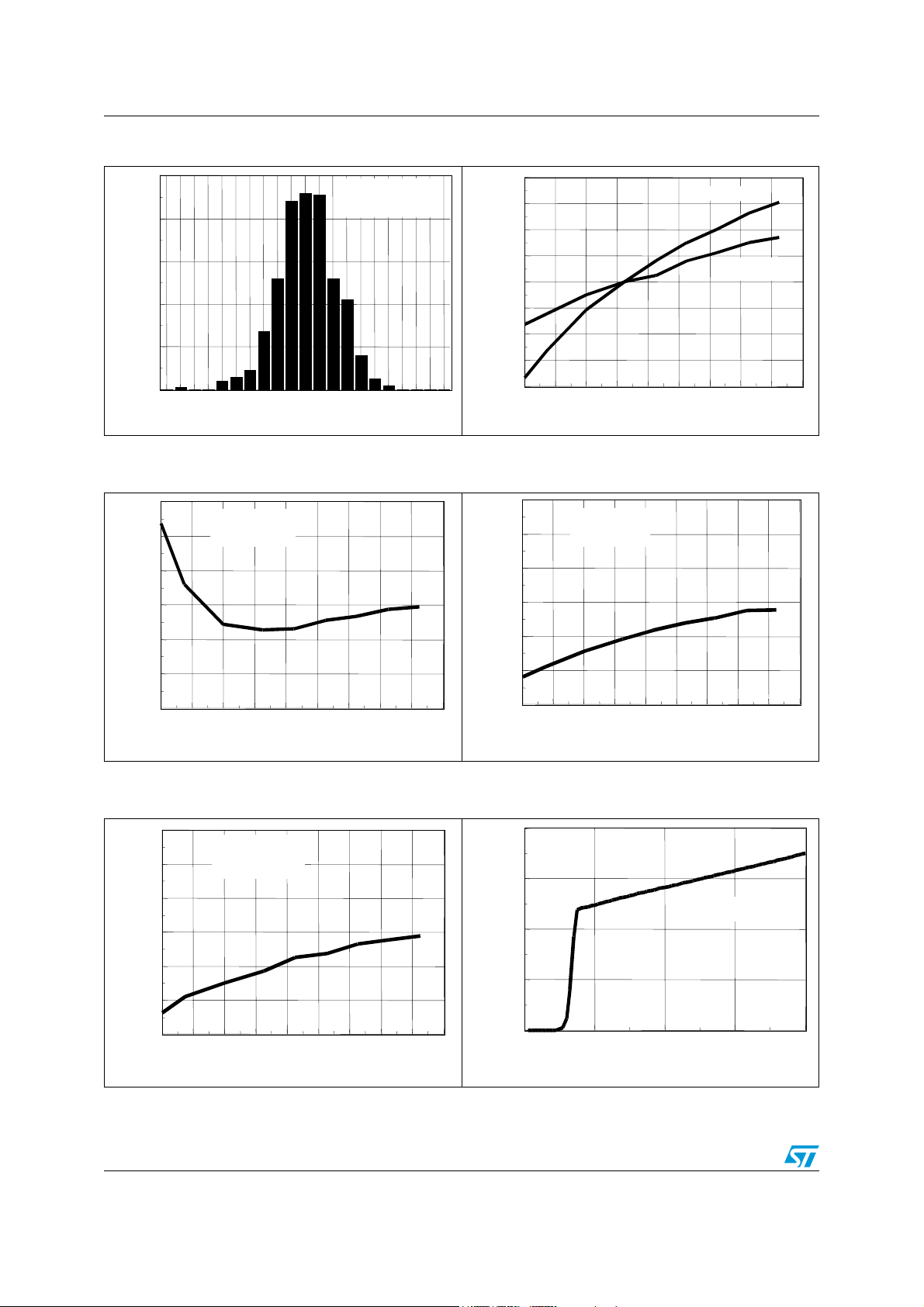
0
Figure 1. Input offset voltage distribution Figure 2. Input offset voltage vs. temperature
100
488 pieces tested
Vcc = 10V
80
60
40
Quantity of Pieces
20
0
-2. -1.6 -1.2 -.8 -.4 0 .4 .8 1.2 1.6 2
Input Offset Voltage (mV)
Temp = +25°C
Figure 3. Input bias current vs. temperature
at Vcc = 1.8 V
0
Vcc = 1.8V
-2
-4
Vicm = 0.9V
400
300
200
100
0
-100
-200
Input Voltage Drift (µV)
-300
-400
-40
-20
0
20
40
Temperature (°C)
Vcc = 1.8V
60
80
Vcc = 10V
120
100
Figure 4. Input bias current vs. temperature
at Vcc = 3 V
-2
-4
Vcc = 3V
Vicm = 1.5V
140
-6
-8
Input bias current (nA)
-10
-12
-40
-20
0
20
40
60
80
100
120
140
Temperature (°C)
Figure 5. Input bias current vs. temperature
at Vcc = 5 V
0
Vcc = 5V
-20
Vicm = 2.5V
0
20
40
Temperature (°C)
60
80
100
120
140
-2
-4
-6
-8
Input bias current (nA)
-10
-12
-40
-6
-8
-10
Input bias current (nA)
-12
-40
-20
0
20
40
60
80
100
120
140
Temperature (°C)
Figure 6. Supply current/amplifier vs. supply
voltage
200
150
Tamb = 25°C
100
50
Supply Current (µA)
0
02468
Supply Voltage (V)
8/24 Doc ID 6991 Rev 4
 Loading...