

ST TN1215, TS1220, TYN612, TYN812, TYN1012 User Manual
TN1215, TS1220
TYN612, TYN812, TYN1012
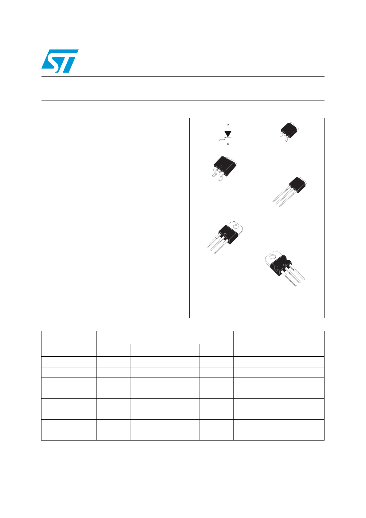
Sensitive and standard 12 A SCRs
Features
■ On-state rms current, I
■ Repetitive peak off-state voltage, V
600 to 1000 V
■ Triggering gate current, I
T(RMS)
0.2 to 15 mA
GT
12 A
DRM/VRRM
Description
Available either in sensitive (TS1220) or standard
(TN1215 / TYNx12) gate triggering levels, the
12 A SCR series is suitable to fit all modes of
control, found in applications such as overvoltage
crowbar protection, motor control circuits in power
tools and kitchen aids, inrush current limiting
circuits, capacitive discharge ignition and voltage
regulation circuits.
Available in through-hole or surface-mount
packages, they provide an optimized performance
in a limited space area.
A
G
K
A
TN1215-xxxB
K
A
G
DPAK
A
TS1220-xxxB
K
A
G
2
PAK
D
A
TN1215-xxxG
TS1220-xxxG
A
K
A
G
IPAK
TN1215-xxxH
TS1220-xxxH
K
A
G
A
TO-220AB
TYNx12RG
TYNx12TRG
G
A
K
TO-220AB
TS1220-xxxT
Table 1. Device summary
Voltage (xxx) V
Order code
600 V 700 V 800 V 1000 V
DRM/VRRM
Sensitivity
IGT
Package
TN1215-xxxB X X 15 mA DPAK
TN1215-xxxG X X 15 mA D
2
PA K
TN1215-xxxH X X 15 mA IPAK
TS1220-xxxB X X 0.2 mA DPAK
TS1220-xxxH X 0.2 mA IPAK
TS1220-xxxT X 0.2 mA TO-220AB
TYNx12RG X X X 15 mA TO-220AB
TYNx12TRG X X X 5 mA TO-220AB
September 2011 Doc ID 7475 Rev 7 1/13
www.st.com
13

Characteristics TN1215, TS1220, TYN612, TYN812, TYN1012
1 Characteristics
Table 2. Absolute ratings (limiting values)
Value
Symbol Parameter
TN1215-G
TYNx12
TN1215-B/-H
TS1220-B/-H/T
Unit
I
T(RMS)
I
T(AV)
I
TSM
dI/dt
I
GM
P
G(AV)
T
V
RGM
Table 3. Sensitive electrical characteristics (Tj = 25 °C, unless otherwise specified)
RMS on-state current (180 °Conduction angle) Tc = 105 °C 12 A
Average on-state current (180 °Conduction angle) Tc = 105 °C 8 A
Non repetitive surge peak on-state
current
²
²
tI
I
t Value for fusing tp = 10 ms Tj = 25 °C 98 60 A
Critical rate of rise of on-state
current I
= 2 x IGT, tr ≤ 100 ns
G
= 8.3 ms
t
p
= 10 ms 140 110
t
p
F = 60 Hz T
= 25 °C
T
j
= 125 °C 50 A/µs
j
145 115
Peak gate current tp = 20 µs Tj = 125 °C 4 A
Average gate power dissipation Tj = 125 °C 1 W
Storage junction temperature range
stg
T
Operating junction temperature range
j
Maximum peak reverse gate voltage
(for TN1215 and TYNx12 only)
- 40 to + 150
- 40 to + 125
5V
Symbol Test conditions TS1220 Unit
I
GT
V
GT
V
GD
V
RGIRG
I
H
I
L
dV/dt V
V
TM
V
t0
R
d
I
DRM
I
RRM
VD = 12 V, RL = 140 Ω
VD = V
DRM, RL
= 3.3 kΩ, RGK = 220 Ω Tj = 125 °C MIN. 0.1 V
= 10 µA MIN. 8 V
IT = 50 mA, RGK = 1 kΩ MAX. 5 mA
IG = 1 mA, RGK = 1 kΩ MAX. 6 mA
= 65 % V
D
DRM, RGK
= 220 Ω Tj = 125 °C MIN. 5 V/µs
ITM = 24 A, tp = 380 µs Tj = 25 °C MAX. 1.6 V
Threshold voltage Tj = 125 °C MAX. 0.85 V
Dynamic resistance Tj = 125 °C MAX. 30 mΩ
T
= 25 °C
V
DRM
= V
, RGK = 220 Ω
RRM
j
= 125 °C 2 mA
T
j
MAX. 200 µA
MAX. 0.8 V
5µA
MAX.
A
°C
2
S
2/13 Doc ID 7475 Rev 7
TN1215, TS1220, TYN612, TYN812, TYN1012 Characteristics
Table 4. Standard electrical characteristics (Tj = 25 °C, unless otherwise specified)
TN1215 TYN
Symbol Test conditions
B / H G x12T x12
Unit
I
GT
V
V
I
dV/dt V
V
V
R
I
DRM
I
RRM
Table 5. Thermal resistance
VD = 12 V RL = 33 Ω
GT
VD = V
GD
IT = 500 mA Gate open MAX. 40 30 15 30 mA
H
IG = 1.2 I
I
L
= 67 % V
D
ITM = 24 A tp = 380 µs Tj = 25 °C MAX. 1.6 V
TM
Threshold voltage Tj = 125 °C MAX. 0.85 V
t0
Dynamic resistance Tj = 125 °C MAX. 30 mΩ
d
RL = 3.3 kΩ Tj = 125 °C MIN. 0.2 V
DRM
GT
Gate open Tj =125 °C MIN. 200 40 200 V/µs
DRM
Tj = 25 °C
V
= V
DRM
RRM
T
= 125 °C 2 mA
j
MAX. 15 5 15
MAX. 1.3 V
MAX. 80 60 30 60 mA
5µA
MAX.
Symbol Parameter Value Unit
MIN. 2 0.5 2
R
R
th(j-c)
th(j-a)
Junction to case (DC) 1.3 °C/W
(1)
= 0.5 cm²DPAK 70
S
(1)
S
= 1 cm²D2PA K 4 5
Junction to ambient (DC)
IPAK 100
mA
°C/W
1. S = Copper surface under tab
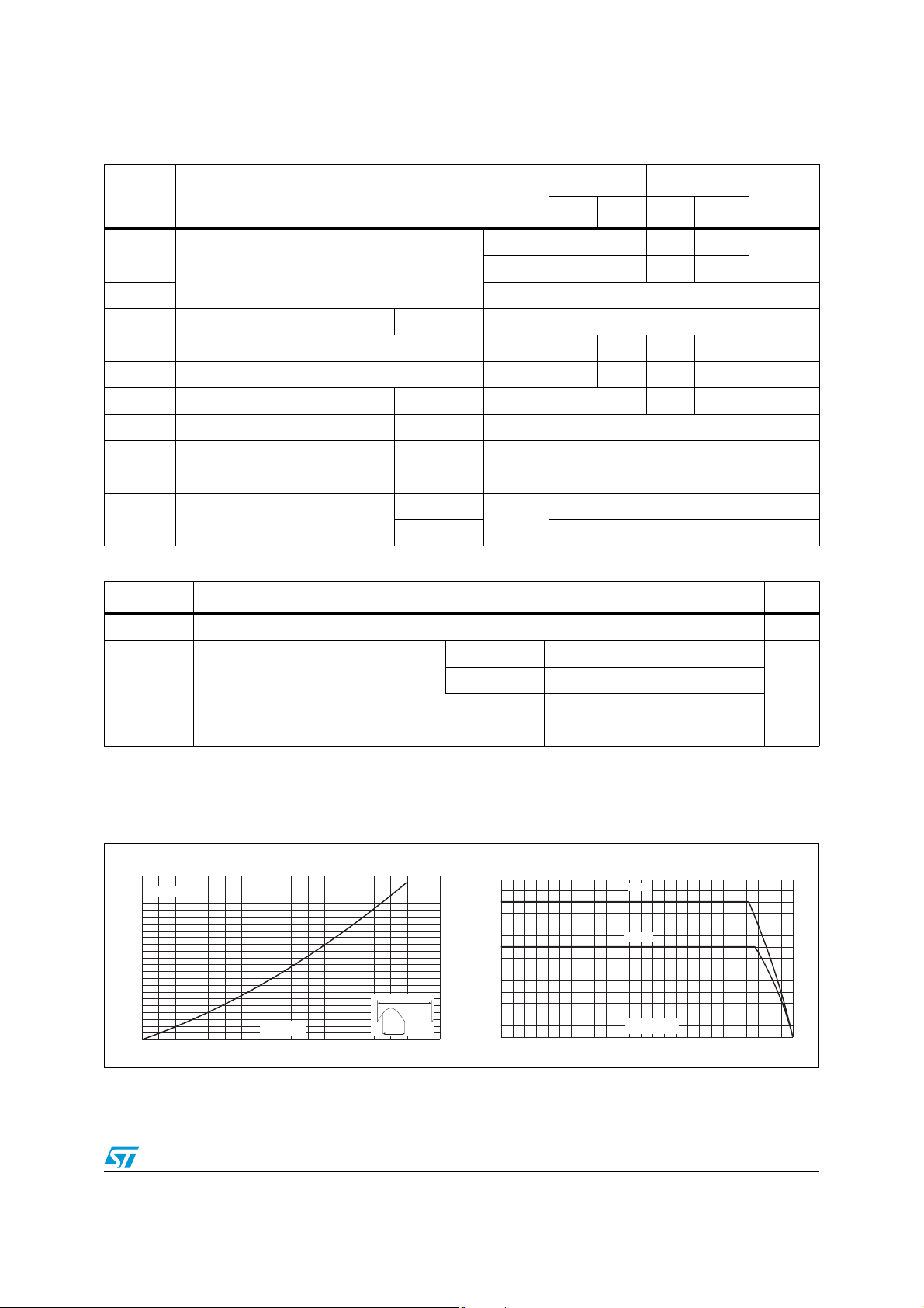
Figure 1. Maximum average power
dissipation versus average
on-state current
P(W)
12
11
α = 180°
10
9
8
7
6
5
4
3
2
1
0
0123456789
I (A)
T(AV)
TO-220AB 60
Figure 2. Average and DC on-state current
versus case temperature
I (A)
T(AV)
14
12
10
8
6
360°
α
4
2
0
0 25 50 75 100 125
Doc ID 7475 Rev 7 3/13
D.C.
α = 180°
T (°C)
case
Characteristics TN1215, TS1220, TYN612, TYN812, TYN1012
Figure 3. Average and D.C. on-state current
versus ambient temperature
(DPAK)
I (A)
T(AV)
3.0
Device mounted on FR4 with
2.5
2.0
1.5
α = 180°
1.0
0.5
0.0
0 25 50 75 100 125
D.C.
2
DPAK
DPAK
T (°C)
recommended pad layout
amb
Figure 5. Relative variation of thermal
impedance junction to ambient
versus pulse duration (DPAK)
K=[Z /R
1.00
0.10
0.01
th(j-a) th(j-a)
Device mounted on FR4 with
recommended pad layout
1E-2 1E-1 1E+0 1E+1 1E+2 5E+2
]
2
DPAK
DPAK
t (s)
p
TO-220AB / IPAK
Figure 4. Relative variation of thermal
impedance junction to case versus
pulse duration
K=[Z /R
th(j-c) th(j-c)
1.0
0.5
0.2
0.1
1E-3 1E-2 1E-1 1E+0
]
t (s)
p
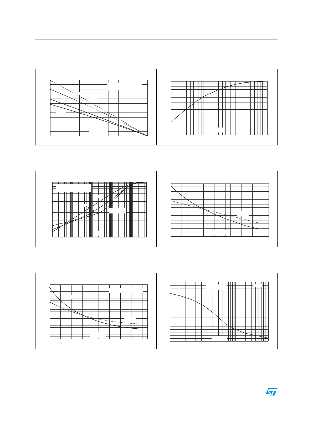
Figure 6. Relative variation of gate trigger
and holding current versus junction
temperature for TS1220 series
I,I,I[T] /
GTHL j
2.0
1.8
1.6
1.4
1.2
1.0
0.8
0.6
0.4
0.2
0.0
-40 -20 0 20 40 60 80 100 120 140
I ,I ,I [T =25°C]
GT H L j
I
GT
T (°C)
j
IH& I
R = 1k
GK
L
Ω
Figure 7. Relative variation of gate trigger
Figure 8. Relative variation of holding
and holding current versus junction
temperature
I [R ] / I [ =1k ]
I,I,I[T] /
GTHL j
2.4
2.2
2.0
1.8
1.6
1.4
1.2
1.0
0.8
0.6
0.4
0.2
0.0
-40 -20 0 20 40 60 80 100 120 140
I ,I ,I [T =25°C]
GTHL j
I
GT
T (°C)
j
TN1215 and TYNx12 Series
IH& I
L
4/13 Doc ID 7475 Rev 7
HGK HΩRGK
5.0
4.5
4.0
3.5
3.0
2.5
2.0
1.5
1.0
0.5
0.0
1E-2 1E-1 1E+0 1E+1
current versus gate-cathode
resistance (typical values)
TS1220 Series
R(k)GKΩ
Tj= 25°C
 Loading...