

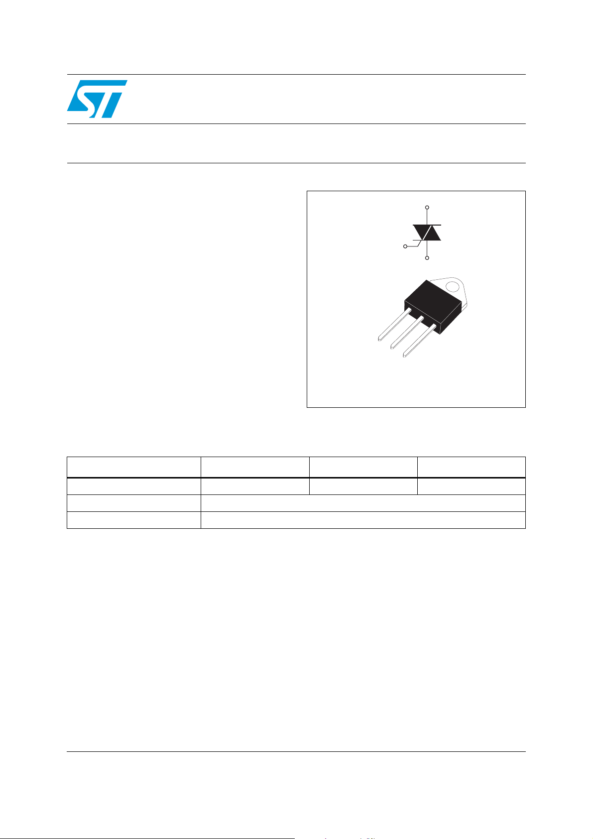
TPDVxx40
40 A high voltage Triacs
Features
■ On-state current (I
■ Max. blocking voltage (V
■ Gate current (I
■ Commutation @ 10 V/µs: up to 142 A/ms
■ Noise immunity: 500 V/µs
■ insulated package:
): 200 mA
GT
– 2,500 V rms (UL recognized: E81734).
T(RMS)
): 40 A
DRM/VRRM
): 1200 V
Description
The TPDVxx40 series use a high performance
alternistor technology.
Featuring very high commutation levels and high
surge current capability, this family is well adapted
to power control on inductive load (motor,
transformer...)
Table 1. Device summary
Parameter TPDV640RG TPDV840RG TPDV1240RG
Blocking voltage V
On-state current I
Gate current I
GT
DRM/VRRM
T(RMS)
600 V 800 V 1200 V
A1
40 A
200 mA
A2
G
A1
A2
G
TOP3 insulated
March 2011 Doc ID 18270 Rev 1 1/7
www.st.com
7
Characteristics TPDVxx40
1 Characteristics
Table 2. Absolute ratings (limiting values)
Symbol Parameter Value Unit
I
T(RMS)
I
TSM
2
I
tI
dI/dt
V
DRM
V
RRM
On-state rms current (180° conduction angle) Tc = 75 °C 40 A
= 2.5 ms
t
Non repetitive surge peak on-state
current
2
t value for fusing tp = 10 ms Tj = 25 °C 610 A2S
Critical rate of rise of on-state current
IG = 500 mA , dIG/dt = 1 A/µs
p
= 25 °C
T
j
= 10 ms 350
t
p
Repetitive F = 50 Hz 20
Non repetitive 100
TPDV640
Repetitive peak off-state voltage
Tj = 125 °C
590
600
TPDV1240 1200
T
stg
T
j
T
L
V
INS(RMS)
1. A1, A2, gate terminals to case for 1 minute
Table 3. Electrical Characteristics (Tj = 25 °C, unless otherwise specified)
Storage junction temperature range
Operating junction temperature range
- 40 to + 150
- 40 to + 125
Maximum lead temperature for soldering during 10s at 2mm from case 260 °C
(1)
Insulation rms voltage 2500 V
Atp = 8.3 ms 370
A/µs
VTPDV840 800
°C
Symbol Test conditions Quadrant Value Unit
I
GT
V
GT
V
GD
t
gt
(1)
I
H
I
L
dV/dt
V
TM
I
DRM
I
RRM
(dI/dt)c
VD = 12 V DC, RL = 33 Ω I - II - III
VD = V
VD = V
RL = 3.3 kΩ T
DRM
= 500 mA dIG/dt = 3 A/µs I - II - III TYP. 2.5 µs
DRM IG
= 125 °C I - II - III MIN. 0.2 V
j
IT = 500 mA Gate open MAX. 50 mA
I - III
IG = 1.2 x IGT
II 200
Linear slope up to:
= 67 % V
V
D
(1)
ITM = 35 A tp = 380 µs MAX. 1.8 V
Gate open
DRM
T
= 125 °C MIN. 500 V/µs
j
Tj = 25 °C
V
= V
DRM
(dV/dt)c = 200 V/µs
(1)
RRM
= 125 °C 8 mA
T
j
Tj = 125 °C MIN.
MAX. 200 mA
MAX. 1.5 V
100
TYP.
20 µA
MAX.
35
(dV/dt)c = 10 V/µs 142
1. For either polarity of electrode A2 voltage with reference to electrode A1.
mA
A/ms
2/7 Doc ID 18270 Rev 1
TPDVxx40 Characteristics
Table 4. Gate characteristics (maximum values)
Symbol Parameter Value Unit
P
G(AV)
P
GM
I
GM
V
GM
Table 5. Thermal resistance
Average gate power dissipation 1 W
Peak gate power dissipation tp = 20 µs 40 W
Peak gate current tp = 20 µs 8 A
Peak positive gate voltage tp = 20 µs 16 V
Symbol Parameter Value Unit
R
th(j-a)
R
th(j-c)
R
th(j-c)
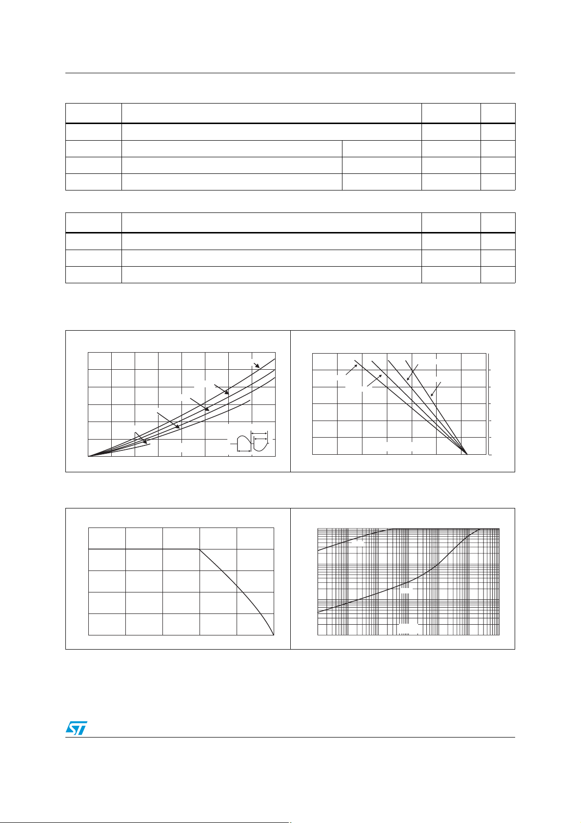
Figure 1. Max. rms power dissipation versus
P(W)
60
50
40
30
20
10
0
0 5 10 15 20 25 30 35 40
Junction to ambient 50 °C/W
DC Junction to case for DC 1.2 °C/W
AC Junction to case for 360 °Conduction angle (F = 50 Hz) 0.9 °C/W
Figure 2. Max. rms power dissipation and
on-state rms current (F = 50 Hz).
(curves limited by (dI/dt)c)
α = 180°
α = 120°
α = 90°
α = 60°
α = 30°
I (A)
T(RMS)
180°
α
α
P(W)
60
50
40
30
20
10
0
0 20 40 60 80 100 120 140
max. allowable temperatures
(T
R = 0.75°C/W
th
amb
R = 0.5°C/W
th
and T
T (°C)
amb
case
R = 0.25°C/W
th
) for various R
R = 0°C/W
th
T (°C)
th
case
75
85
95
105
115
125
Figure 3. On-state rms current versus case
temperature
I (A)
T(RMS)
50
40
30
20
10
0
025 7550 100 125
α = 180°
T (°C)
case
Doc ID 18270 Rev 1 3/7
Figure 4. Relative variation of thermal
impedance versus pulse duration
K=[Z /R
th(j-c) th(j-c)
1.00
0.10
0.01
0.0
1E-3 1E-2 1E-1 1E+0 1E+1 1E+2 1E+3
]
Z
th(j-c)
Z
th(j-a)
t (s)
p
 Loading...