

Features
■ High clamping voltage structure
(1200 to 1500 V)
■ Low gate triggering current for direct drive from
line (< 1.5 mA)
■ High holding current (> 175 mA), ensuring high
striking energy
Description
The TN22 has been specifically developed for use
in tube lamp electronic starter circuits.
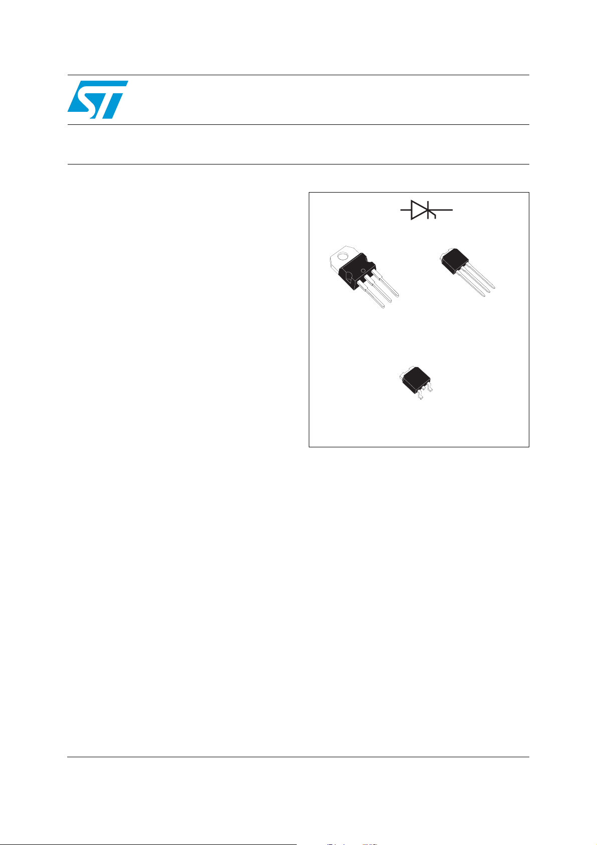
TN22
Fluorescent tube lamp starter SCR
1
3
TAB
IPAK
TN22-1500H
3
2
1
TAB
TO-220AB
TN22-1500T
2, TAB
1
3
2
Used in conjunction with a sensitive SCR, it
provides high energy striking characteristics with
low triggering power.
Thanks to the optimized characteristics of the
TN22, starters based on this device can offer high
reliability levels and extended life time of the
fluorescent tube lamps.
TAB
2
3
1
DPAK
TN22-1500B-TR
August 2009 Doc ID 3768 Rev 3 1/13
www.st.com
13
Characteristics TN22
1 Characteristics
Table 1. Absolute ratings (limiting values)
Symbol Parameter Value Unit
V
I
T(RMS)
I
T(AV)
I
dl/dt
P
G(AV)
P
I
V
T
Table 2. Electrical characteristics (Tj = 25 °C unless otherwise stated)
Repetitive peak off-state voltage Tj = 110 °C 400 V
RRM
On-state rms current
full sine wave (180° conduction angle)
Mean on-state current
Full sinewave (180° conduction angle)
Non repetitive surge peak on-state current
TSM
(Tj initial = 25 °C)
2
tI2t Value for fusing tp = 10 ms 2 A2s
I
Critical rate of rise of on-state current
= 5 mA dIG/dt = 70 mA/µs
I
G
= 95 °C 2 A
T
c
T
= 95 °C 1.8 A
c
t
= 8.3 ms 22
p
t
= 10 ms 20
p
50 A/µs
Average gate power dissipation 300 mW
= 20 µs
Peak gate power dissipation
GM
Peak gate current
GM
Maximum peak reverse gate voltage 6 V
RGM
stg
Storage and operating junction temperature range
T
j
Maximum lead temperature for soldering during 10 s at 4.5 mm
T
L
from case
t
p
= 20 µs
t
p
2W
1A
-40 to +150
-40 to +110
260 °C
Symbol Test conditions Value Unit
I
V
dV/dt Linear slope up to V
V
Table 3. Static electrical characteristics (Tj = 25 °C unless otherwise stated)
VD=12 V (DC), RL= 33 Ω MAX 1.5 mA
GT
VD=12 V (DC), RL= 33 Ω, RGK = 1 KΩ MAX 3 V
GT
VGK = 0 V MIN 175 mA
I
H
BRID
= 5 mA, VGK = 0 V
= 67% V
D
DRM, VGK
= 0 V, Tj = 110 °C MIN 500 V/µs
MIN 1200
MAX 1500
Symbol Test conditions Value Unit
V
TMITM
I
DRMVDRM
Table 4. Thermal resistance
= 2 A tp = 380 µs MAX 3.1 V
rated MAX 0.1 mA
Symbol Parameter Value Unit
A
°C
V
R
R
th(j-a)
Junction to ambient
Junction to case 3 °C/W
th(j-c)
2/13 Doc ID 3768 Rev 3
DPAK / IPAK 100
TO-220AB 60
°C/W
TN22 Characteristics
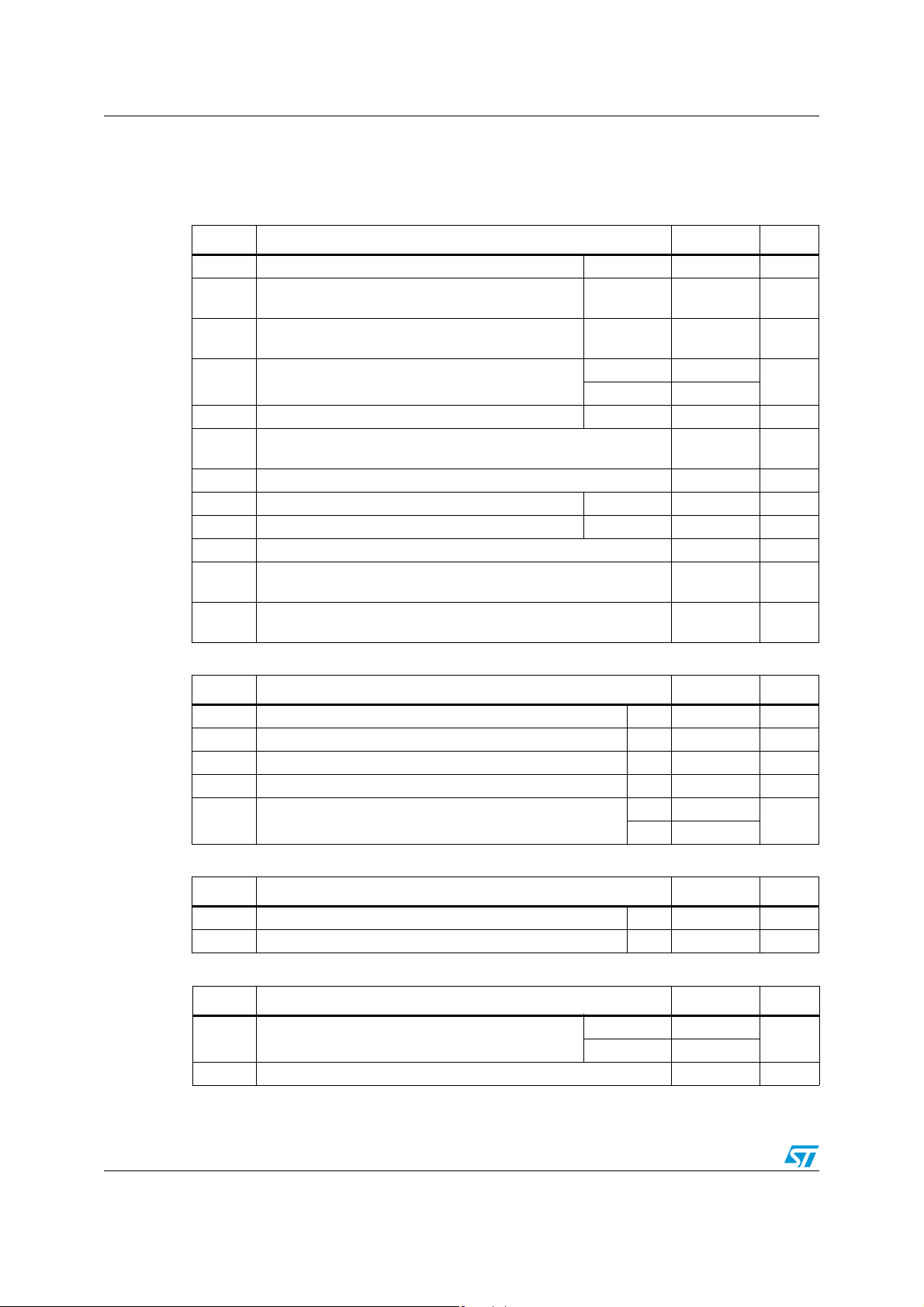
Figure 1. Maximum average power
dissipation versus average on-state
current (rectified sine wave)
P(W)
6
5
4
3
2
1
0
0.0 0.2 0.4 0.6 0.8 1.0 1.2 1.4 1.6 1.8 2.0
α=30 °
I
T(AV)
α=60 °
(A)
α=90 °
α=120 °
α=180 °
360°360°360°360°
Figure 3. Average on-state current versus
ambient temperature, free air
convection (rectified full sine wave)
I
(A)
T(AV)
0.7
TO-220AB
0.6
0.5
0.4
0.3
DPAK / IPAK
0.2
0.1
0.0
0 102030405060 708090100110
T
(°C)
amb
α=180°
Figure 5. Relative variation of gate trigger
current and holding current versus
junction temperature
IGT,IH[Tj]/IGT,IH[Tj=25°C]
2.4
2.2
2.0
1.8
1.6
1.4
1.2
1.0
0.8
0.6
0.4
0.2
0.0
I
GT
I
H
-40 -30 -20 -10 0 10 20 30 40 50 60 70 80 90 100 110 120 130
typical values
Tj(°C)
Figure 2. Average on-state current versus
case temperature
(rectified full sine wave)
I
(A)
T(AV)
2.0
1.8
1.6
1.4
1.2
1.0
0.8
0.6
0.4
0.2
0.0
360°360°360°360°
0 102030405060 708090100110
α=180 °
TC(°C)
Figure 4. Variation of thermal impedance
junction to ambient versus pulse
duration
Z
(°C/W)
th(j-a)
100.0
10.0
1.0
0.1
1.E-03 1.E-02 1.E-01 1.E+00 1.E+01 1.E+02 1.E+03
tP(s)
DPAK
IPAK
TO-220AB
Figure 6. Surge peak on-state current versus
number of cycles
I
(A)
TSM
22
20
18
16
14
12
10
8
6
4
Tjinitial=25 °C
2
0
1 10 100 1000
Number of cycles
tp=10ms
One cycle
Doc ID 3768 Rev 3 3/13

Characteristics TN22
0
0
0
0
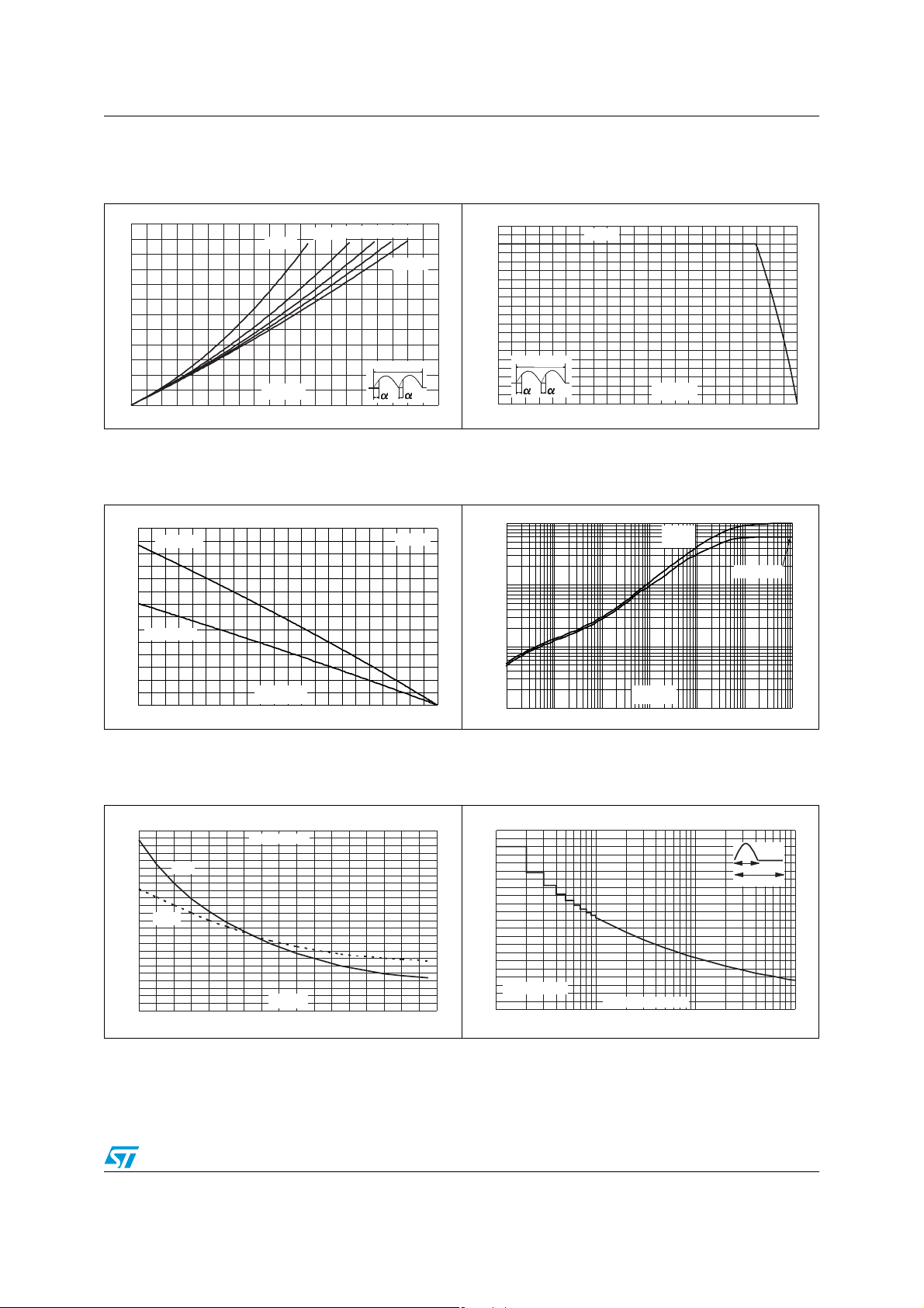
Figure 7. Non-repetitive surge peak on-state
current for a sinusoidal pulse
I
(A), I²t (A²s)
TSM
1000
dI/dt limitation
50 A/µs
100
t < 10 ms and corresponding value of I t
p
10
1
0.01 0.10 1.00 10.00
2
tP(ms)
Tjinitial=25 °C
I
TSM
I²t
Figure 9. Maximum allowable rms current
versus time conduction and initial
case temperature
I
(A)
T(RMS)
10
Tj max= 135 °C (the failure mode will be short circuit)
9
8
7
6
TCinitial=25°C
5
4
3
2
1
0
TCinitial=65°C
.1 1.
TCinitial=45°CTCinitial=45°C
tP(s)
10.
DPAK
IPAK
100.
Figure 8. On-state characteristics
(maximum values)
ITM(A)
100.0
10.0
1.0
0.1
012345678
Tj=110 °C
Tj=25 °C
VTM(V)
Tjmax. :
Vto= 2.5 V
= 235 mΩ
R
D
Figure 10. Maximum allowable rms current
versus time conduction and initial
case temperature
I
(A)
T(RMS)
10
Tj max= 135 °C (the failure mode will be short circuit)
9
8
7
6
5
4
3
2
1
0
0.1 1.0 10.0 100.0
TCinitial=25°C
TCinitial=65°C
TCinitial=45°CTCinitial=45°C
tP(s)
TO-220AB
Figure 11. Holding current versus gate-cathode resistance (typical values)
IH(mA)
1000
100
10
RGK()
1
1 10 100 1000
Ω
4/13 Doc ID 3768 Rev 3
Tj=25 °C

TN22 Application information
FLUORESCENT
TUBE
MAINS
VOLTAGE
SWITCH
INDUCTANCE
BALLAST
Rectifier
Reset control
Ignition circuit
Preheating
time control
Voltage detector
SCR
mains
mains
-
+
D2 – D5
TN22
+
C1
+
C2
R1
R4
R3
R2
D6
D1
I
T
V
S
1
2
3
4
5
Starter circuit
2 Application information
2.1 Overview
The TN22 has been designed for use as a fluorescent tube starter switch.
As shown in Figure 12, the starter circuit is divided in five parts:
1. Rectifier bridge: to rectify mains voltage.
2. Volt a g e dete c to r: RCD circuit used to switch on the TN22.
3. Preheating time control: RC circuit used to switch on the SCR, so turn off the TN22.
4. Ignition circuit: made of sensitive SCR and TN22 devices.
5. Reset control: resistor used to discharge the C2 capacitor and to reset the circuit.
Figure 12. Electronic starter schematic
FLUORESCENT
Preheating
time control
Doc ID 3768 Rev 3 5/13

Application information TN22
Three steps are necessary to ignite a fluorescent tube (see Figure 13):
● preheating of the filament
● ignition of the tube
● "lighting" mode
Figure 13. The three operating steps of the electronic starter:
preheating, ignition and lighting
Preheating
Preheating
Lighting
IT(1 A/div)
IT(1 A/div)
VS(500 V/div)
VS(500 V/div)
Lighting
2.2 Filament and tube preheating
The mains voltage is applied across the circuit and when it reaches a higher level than the
zener clamping voltage (V
The TN22 switches on when the voltage across its gate to cathode junction reaches the
triggering gate level (V
As the TN22 is in on-state, a full sinusoidal current flows through the filaments (primary of
the rectifier bridge) that are warmed up. This current is limited by the input ballast. The TN22
remains on at each current zero crossing point because the gate is still powered by the C1
capacitor.
The preheating time duration is set with the RC circuit made of R3, R2 and C2, and
according to the voltage polarization fixed by the D1 drop voltage.
The preheating time is typically in the range of 2 to 3 seconds depending on the tube
characteristics.
), a current flows through the resistor R1 and the capacitor C1.
CL
).
GT
Ignition
Ignition
6/13 Doc ID 3768 Rev 3

TN22 Application information
2.3 Ignition step
When C2 is charged above the SCR triggering gate voltage (VGT), the SCR switches on.
The voltage across the TN22 gate to cathode junction is fixed to a negative value, which
allows a proper TN22 switch-off, with a high holding current (I
When the current reaches I
, the TN22 switches off and the ballast inductor generates a
H
high voltage pulse across the tube (see Figure 14). This over-voltage is clamped by the
TN22 to a value fixed by the breakdown voltage (V
). A 1200 V to 1500 V level is
BR
necessary to ensure a correct ignition of the fluorescent tubes.
Figure 14. Typical high voltage pulse of an electronic starter circuit
(P0130AA SCR, TN22)
VBR1300 V≈
VS(200 V/div)
IH225 mA≈
IT(50 mA/div)
) level.
H
If the lamp is not ignited after the first pulse, the starter circuit starts a new ignition
sequence. The pulse is regenerated until ignition of the tube lamp. If the lamp is not ignited
after several attempts, the starter circuit can automatically stop the ignition sequence.
Figure 15. Repetitive ignitions sequence
2.4 Lighting state
When the lamp is ignited, the capacitor C2 is discharged through the resistors R2, R3 and
R4. The voltage across the lamp remains lower than the D6 clamping voltage (V
avoiding the triggering of the TN22. The starter circuit remains in stand-by mode.
Pulse
f
BURST
Mains voltage
= 50 Hz
IT(500 mA /div)
VS(500 V/div)
CL
),
Doc ID 3768 Rev 3 7/13

Ordering information scheme TN22
3 Ordering information scheme
Figure 16. Ordering information scheme
TN 2 2 - 1500 x -TR
Startlight device
On-state rms current
2 = 2 A
Triggering gate current (MAX)
2 = 1.5 mA
Breakdown voltage
1500 = 1500 V
Package
B = DPAK
H = IPAK
T = TO-220AB
R = I2PA K
Packing
Blank = Tube
-TR = Tape and reel (DPAK)
8/13 Doc ID 3768 Rev 3

TN22 Package information
4 Package information
● Epoxy meets UL94,V0
● Cooling method: by convection
● Recommended torque value: 0.4 to 0.6 N·m (TO-220AB)
In order to meet environmental requirements, ST offers these devices in different grades of
ECOPACK
specifications, grade definitions and product status are available at: www.st.com
ECOPACK
Table 5. DPAK dimensions
®
packages, depending on their level of environmental compliance. ECOPACK®
®
is an ST trademark.
.
Dimensions
Ref.
Millimeters Inches
Min. Max. Min. Max.
A 2.20 2.40 0.086 0.094
E
B2
L2
H
L4
B
G
A1
A
C2
A1 0.90 1.10 0.035 0.043
A2 0.03 0.23 0.001 0.009
B 0.64 0.90 0.025 0.035
B2 5.20 5.40 0.204 0.212
R
D
C 0.45 0.60 0.017 0.023
C2 0.48 0.60 0.018 0.023
R
C
D 6.00 6.20 0.236 0.244
E 6.40 6.60 0.251 0.259
0.60 MIN.
A2
G 4.40 4.60 0.173 0.181
H 9.35 10.10 0.368 0.397
V2
L2 0.80 typ. 0.031 typ.
L4 0.60 1.00 0.023 0.039
Figure 17. Footprint (dimensions in mm)
6.7 3 3
6.7
Doc ID 3768 Rev 3 9/13
V2 0° 8° 0° 8°
1.6
2.3
2.3
1.6

Package information TN22
Table 6. IPAK dimensions
Dimensions
Ref.
Millimeters Inches
Min. Typ. Max. Min. Typ. Max.
A 2.20 - 2.40 0.086 - 0.094
A1 0.90 - 1.10 0.035 - 0.043
A3 0.70 - 1.30 0.027 - 0.051
A
E
B2
L2
C2
B 0.64 - 0.90 0.025 - 0.035
B2 5.20 - 5.40 0.204 - 0.212
B3 - - 0.95 - - 0.037
B5 - 0.30 - - 0.035 -
D
C 0.45 - 0.60 0.017 - 0.023
C2 0.48 - 0.60 0.019 - 0.023
H
L1
L
B3
B
V1
A1
D 6 - 6.20 0.236 - 0.244
E 6.40 - 6.60 0.252 - 0.260
e - 2.28 - - 0.090 -
B5
e
G
C
A3
G 4.40 - 4.60 0.173 - 0.181
H-16.10- -0.634-
L 9 - 9.40 0.354 - 0.370
L1 0.8 - 1.20 0.031 - 0.047
L2 - 0.80 1 - 0.031 0.039
10/13 Doc ID 3768 Rev 3
V1 - 10° - - 10° -

TN22 Package information
Table 7. TO-220AB dimensions
Dimensions
L2
F2
F1
F
G1
H2
Dia
G
L5
L9
L6
L4
Ref.
Millimeters Inches
Min. Max. Min. Max.
A 4.40 4.60 0.173 0.181
C 1.23 1.32 0.048 0.051
A
C
D 2.40 2.72 0.094 0.107
E 0.49 0.70 0.019 0.027
L7
F 0.61 0.88 0.024 0.034
F1 1.14 1.70 0.044 0.066
F2 1.14 1.70 0.044 0.066
G 4.95 5.15 0.194 0.202
D
G1 2.40 2.70 0.094 0.106
H2 10 10.40 0.393 0.409
L2 16.4 typ. 0.645 typ.
M
E
L4 13 14 0.511 0.551
L5 2.65 2.95 0.104 0.116
L6 15.25 15.75 0.600 0.620
L7 6.20 6.60 0.244 0.259
L9 3.50 3.93 0.137 0.154
M 2.6 typ. 0.102 typ.
Diam. 3.75 3.85 0.147 0.151
Doc ID 3768 Rev 3 11/13

Ordering information TN22
5 Ordering information
Table 8. Ordering information
Order code Marking Package Weight Base qty Delivery mode
TN22-1500B TN22-1500 DPAK 0.3 g 75 Tube
TN22-1500B-TR TN22-1500 DPAK 0.3 g 2500 Tape and reel
TN22-1500H TN22-1500 IPAK 0.4 g 75 Tube
TN22-1500T TN22-1500 TO-220AB 2.0 g 50 Tube
6 Revision history
Table 9. Document revision history
Date Revision Changes
Oct-2000 1 First release.
17-Sep-2005 2 TO-220AB package added.
13-Aug-2009 3 Updated Figure 4. Added Figure 9 and 10.
12/13 Doc ID 3768 Rev 3

TN22
Please Read Carefully:
Information in this document is provided solely in connection with ST products. STMicroelectronics NV and its subsidiaries (“ST”) reserve the
right to make changes, corrections, modifications or improvements, to this document, and the products and services described herein at any
time, without notice.
All ST products are sold pursuant to ST’s terms and conditions of sale.
Purchasers are solely responsible for the choice, selection and use of the ST products and services described herein, and ST assumes no
liability whatsoever relating to the choice, selection or use of the ST products and services described herein.
No license, express or implied, by estoppel or otherwise, to any intellectual property rights is granted under this document. If any part of this
document refers to any third party products or services it shall not be deemed a license grant by ST for the use of such third party products
or services, or any intellectual property contained therein or considered as a warranty covering the use in any manner whatsoever of such
third party products or services or any intellectual property contained therein.
UNLESS OTHERWISE SET FORTH IN ST’S TERMS AND CONDITIONS OF SALE ST DISCLAIMS ANY EXPRESS OR IMPLIED
WARRANTY WITH RESPECT TO THE USE AND/OR SALE OF ST PRODUCTS INCLUDING WITHOUT LIMITATION IMPLIED
WARRANTIES OF MERCHANTABILITY, FITNESS FOR A PARTICULAR PURPOSE (AND THEIR EQUIVALENTS UNDER THE LAWS
OF ANY JURISDICTION), OR INFRINGEMENT OF ANY PATENT, COPYRIGHT OR OTHER INTELLECTUAL PROPERTY RIGHT.
UNLESS EXPRESSLY APPROVED IN WRITING BY AN AUTHORIZED ST REPRESENTATIVE, ST PRODUCTS ARE NOT
RECOMMENDED, AUTHORIZED OR WARRANTED FOR USE IN MILITARY, AIR CRAFT, SPACE, LIFE SAVING, OR LIFE SUSTAINING
APPLICATIONS, NOR IN PRODUCTS OR SYSTEMS WHERE FAILURE OR MALFUNCTION MAY RESULT IN PERSONAL INJURY,
DEATH, OR SEVERE PROPERTY OR ENVIRONMENTAL DAMAGE. ST PRODUCTS WHICH ARE NOT SPECIFIED AS "AUTOMOTIVE
GRADE" MAY ONLY BE USED IN AUTOMOTIVE APPLICATIONS AT USER’S OWN RISK.
Resale of ST products with provisions different from the statements and/or technical features set forth in this document shall immediately void
any warranty granted by ST for the ST product or service described herein and shall not create or extend in any manner whatsoever, any
liability of ST.
ST and the ST logo are trademarks or registered trademarks of ST in various countries.
Information in this document supersedes and replaces all information previously supplied.
The ST logo is a registered trademark of STMicroelectronics. All other names are the property of their respective owners.
© 2009 STMicroelectronics - All rights reserved
STMicroelectronics group of companies
Australia - Belgium - Brazil - Canada - China - Czech Republic - Finland - France - Germany - Hong Kong - India - Israel - Italy - Japan -
Malaysia - Malta - Morocco - Philippines - Singapore - Spain - Sweden - Switzerland - United Kingdom - United States of America
www.st.com
Doc ID 3768 Rev 3 13/13
 Loading...