

Page 1

TN1337
Technical note
SPC58EHx/SPC58NHx giga Ethernet TX_CLK DoS analysis
Introduction
The SPC58EHx/SPC58NHx microcontroller (MCU) embeds the 1 Gbps Ethernet controller RGMII compliant.
This microcontroller introduces a new clock schema designed to manage the RGMII. The RGMII clock schema is designed
to be very flexible and it supports several different programming modes as described in the reference manual (see
Section A.2 Reference documents). The SPC58EHx/SPC58NHx microcontroller has a new dedicated PLL_ETH and a logic to
introduce a delay on the TX_CLK signal. While negotiating the 1000 link speed an improper or not enough margin to align the
data to the clock can make unstable or unusable the whole network connectivity. So, the delay on source is designed to provide
a phase shift of 90 degree guaranteeing enough margin to toggle the data.
The purpose of this technical note is to detail some measurements performed on the SPC58NHADPT302S evaluation board in
order to demonstrate the delay on source functionality applied on the TX_CLK. The document also provides some information
and some examples about the solutions that can be adopted to introduce skew.
TN1337 - Rev 1 - January 2021
For further information contact your local STMicroelectronics sales office.
www.st.com
Page 2
1 RGMII overview
The Reduced Gigabit Media Independent Interface (RGMII) has become a widely used alternative to the Gigabit
Media Independent Interface (GMII) by offering lower pin count.
The RGMII standard achieves this by reducing the width of the parallel data bus and through double data rate
(DDR). RGMII specifies that the clock and data will be generated simultaneously from the transmitting source and
that a skew has to be introduced between clock and data. Skew can be achieved from the transceiver either using
an internal delay or via PCB trace routing.
The interface definition supports two delay modes:
• Delay on Destination (DoD): the delay of the clock signal has to be accomplished by the receiver device.
• Delay on Source (DoS): the transmitter device already provides a delayed clock signal.
The SPC58EHx/SPC58NHx microcontroller has DoS capability as described in the following chapters.
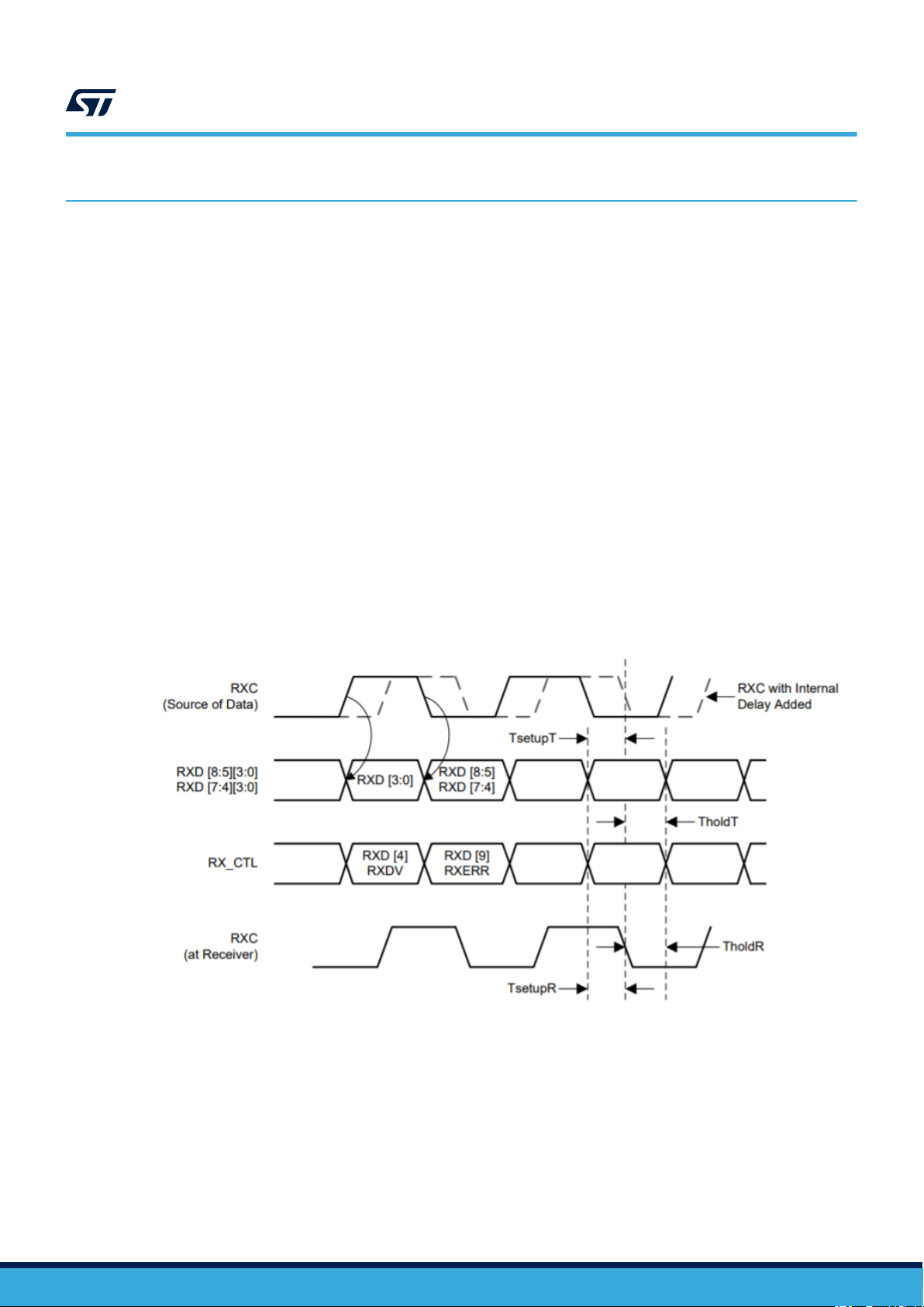
1.1 RGMII timing specification
The RGMII version 2.0 specification defines RGMII data-clock imbalances only for operation at 1000 Mbps, which
uses both clock edges to sample data and control signals at the clock rate of 125 MHz (8 ns period). For 10/100
Mbps operations, the data signals are sampled on the rising clock edge and the control signals are sampled on
both clock edges.
With slower clock rates, 2.5 MHz for 10 Mbps and 25 MHz for 100 Mbps, RGMII imbalances for 10/100 Mbps
operations will have larger timing margins than running at 1000 Mbps, and therefore can be relaxed, such as
maximum value, from 2.6 ns from 1000 Mbps to 160 ns for 10 Mbps and 16 ns for 100 Mbps.
TN1337
RGMII overview
Figure 1. RGMII RX timing diagram
TN1337 - Rev 1
page 2/19
Page 3
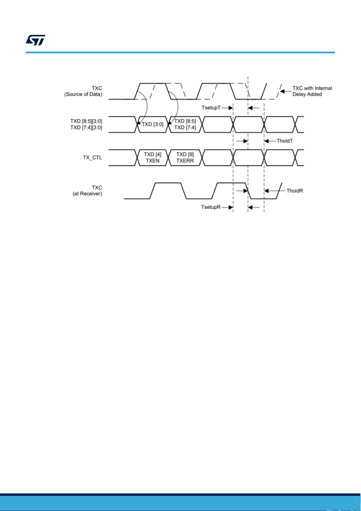
Figure 2. RGMII TX Timing diagram
TN1337
RGMII timing specification
TN1337 - Rev 1
page 3/19
Page 4
SPC58EHx/SPC58NHx RGMII clocking schema
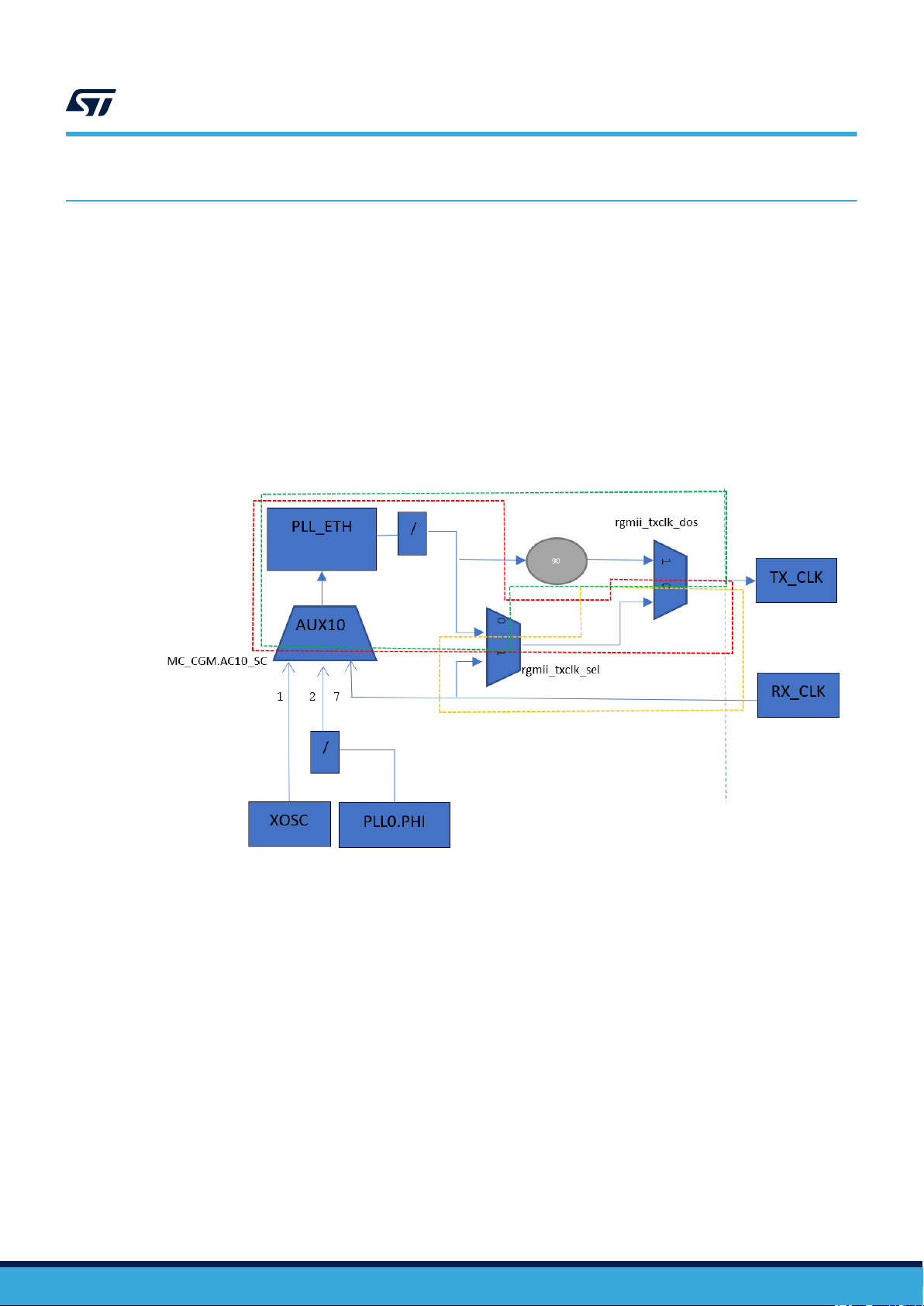
2 SPC58EHx/SPC58NHx RGMII clocking schema
The TX_CLK can be selected using an internal PLL_ETH clock or the receive clock that is routed by the PHY
transceive. When PLL_ETH is selected as reference clock for TX_CLK, MC_CGM Aux10 must be programmed
to configure the reference clock for this source. Check the reference manual (see Section A.2 Reference
documents) for detailed information on MC_CGM module.
There are three possibilities:
• XOSC
• a divided version of PLL0
• a divided version of RXCLK
The delay on the source can be enabled by programming the related mux: rgmii_txclk_dos.
The following figure shows the clock diagram for the RGMII clock selections and DoS clock selection:
Figure 3. SPC58EHx RGMII clock schema
TN1337
2.1 TX_CLK selection with Delay on Source (DoS)
DoS selection is the recommended configuration on this platform and can be performed referring to
Figure 3. SPC58EHx RGMII clock schema, by setting the rgmii_txclk_dos = 1 and rgmii_txclk_sel = 0.
2.2 TX_CLK selection with Delay on Destination (DoD)
In this mode no delay is introduced internally by the microcontroller.
This mode can be activated by:
• selecting the RX_CLK as TX_CLK (both for MAC / PHY)
– rgmii_txclk_dos=0
– rgmii_txclk_sel=1
• selecting the ETH_PLL divided output as TX_CLK
– rgmii_txclk_dos=0
– rgmii_txclk_sel=0
TN1337 - Rev 1
page 4/19
Page 5

3 Microchip KSZ9031RNX RGMII transceiver
The KSZ9031RNX RGMII microchip complies with the timing requirements in the RGMII specification version 2.0
for internal PHY chip delay. For the transmission path, that is from MAC to KSZ9031RNX, the PHY transceiver
by default does not add any delay to its GTX CLK, TEN and data lines. The GTX CLK delay is expected to be
provided by the MAC.
The GTX_CLK on the transceiver is wired to the TX_CLK on the MAC side.It has been verified that, without DoS
selection, on the SPC58NHADPT302S board, used as the reference PCB in these experiments, it is mandatory to
program the KSZ9031RNX to add an additional delay when the giga link speed is negotiated. Without any delay
on TX_CLK, issues occurred when ping the interface from a remote host, e.g. packet lost or no connectivity (see
Section Appendix A Network setup).
In case of DoS selection, it has been demonstrated that the PHY does not need to introduce any further delay, so
the microcontroller DoS logic satisfy the requirements. It does not need any extra delay on 100 Mbps speed .
3.1 GTX_CLK delay from transceiver registers
In case of DoD, MAC does not provide any delay for the TX_CLK, the KSZ9031RNX can be used to provide it.
In fact, the KSZ9031RNX has skew pad registers for all RGMII pins (clock, control signals and data) to provide
programming options to adjust or correct the timing relationship for each RGMII pin.
Here is a piece of the code invoked by the low-level driver to provide the delay on TX_CLK:
TN1337
Microchip KSZ9031RNX RGMII transceiver
#define MMD2_RGMII_CTRL_PAD_SKEW 4
#define MMD2_RGMII_RXDATA_PAD_SKEW 5
#define MMD2_RGMII_TXDATA_PAD_SKEW 6
#define MMD2_RGMII_GTX_CLK_PAD_SKEW 8
#define SPC5_RGMII_RX_CTL_VALUE 0
#define SPC5_RGMII_TX_CTL_VALUE 0
#define SPC5_RGMII_RXDATA_VALUE 0
#define SPC5_RGMII_TXDATA_VALUE 0
#define SPC5_RGMII_GTX_RX_CTL_VALUE 16
#define SPC5_RGMII_GTX_TX_CTL_VALUE (16 << 5) // 0.96ns
if (phydev->speed == SPEED_1000) {
ksz9031_rgmii_pad_skew(phydev,MMD2_RGMII_CTRL_PAD_SKEW,
(SPC5_RGMII_RX_CTL_VALUE | SPC5_RGMII_TX_CTL_VALUE));
ksz9031_rgmii_pad_skew(phydev,MMD2_RGMII_RXDATA_PAD_SKEW,
SPC5_RGMII_RXDATA_VALUE);
ksz9031_rgmii_pad_skew(phydev,MMD2_RGMII_TXDATA_PAD_SKEW,
SPC5_RGMII_TXDATA_VALUE);
ksz9031_rgmii_pad_skew(phydev, MMD2_RGMII_GTX_CLK_PAD_SKEW,
(SPC5_RGMII_GTX_RX_CTL_VALUE|
SPC5_RGMII_GTX_TX_CTL_VALUE));
}
Where:
static void ksz9031_rgmii_pad_skew(struct phy_device *phydev,
uint16_t reg, uint16_t delay)
{
int value;
TN1337 - Rev 1
/* RGMII Control Signal Pad Skew */
value = ksz9031_extended_read(phydev, 1, 2, reg);
value |= delay;
ksz9031_extended_write(phydev, 1, 2, reg, value);
value = ksz9031_extended_read(phydev, 1, 2, reg);
}
page 5/19
Page 6
TN1337
PCB trace routing on GTX_CLK
Note: the transceiver software set is available within the SPC5Studio tool (https://www.st.com/en/development-tools/
spc5-studio.html).
3.2 PCB trace routing on GTX_CLK
The additional delay can be solved in the PCB. In this scenario, neither the PHY transceiver nor the MCU for DoS
may need to be programmed.
The figure below shows an example of another PCB where the tune is created by a serpentine trace route on
GTX_CLK for the KSZ9031RNX with a fixed length of 1 ns (how to calculate it is out of scope of this document).
Figure 4. PCB trace routing on GTX_CLK
TN1337 - Rev 1
page 6/19
Page 7
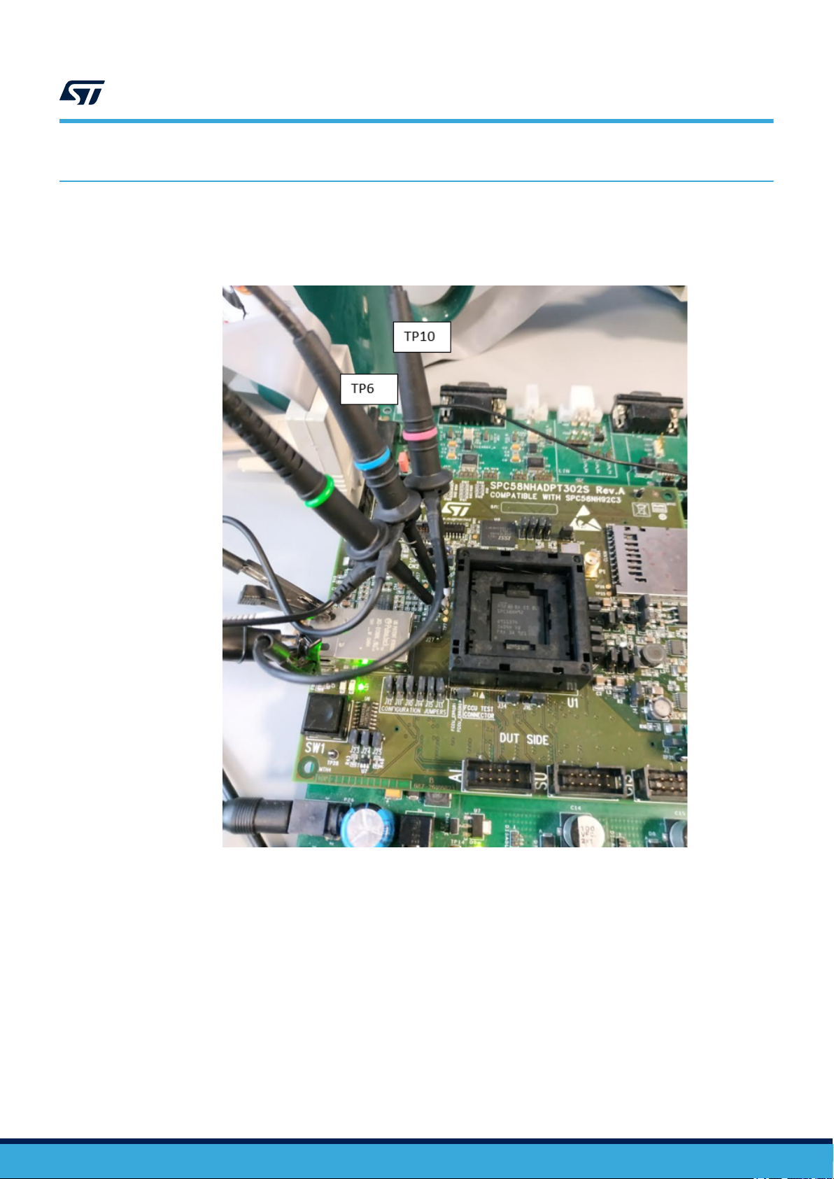
4 Hardware
The figure below shows the SPC58NHADPT302S board used to perform measurements and connections with the
oscilloscope: LeCroy 610Zi using PP008 probes.
TN1337
Hardware
Figure 5. SPC58NHADPT302S connections
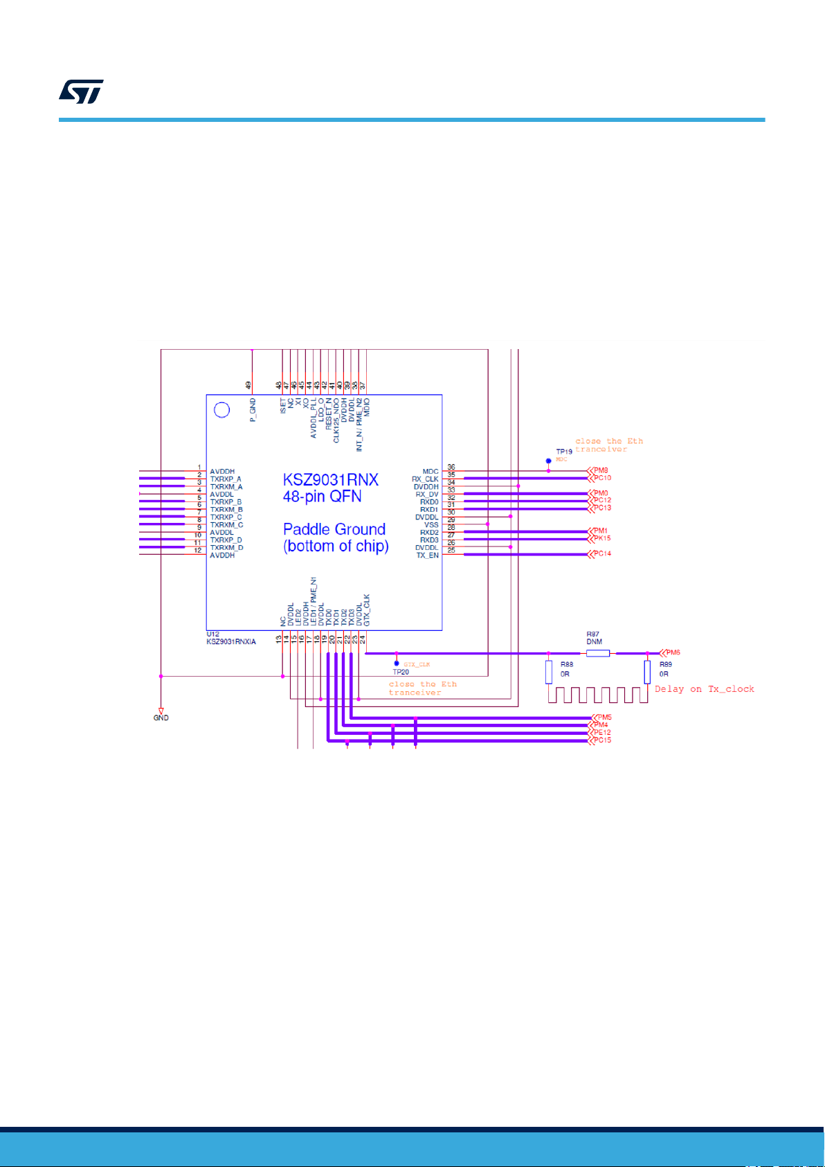
Note: the measurements are taken from GTX_CLK (TP10) and TDX0 (TP6).
Note: all the experiments confirmed that same results are obtained while probing other data signals.
TN1337 - Rev 1
page 7/19
Page 8

Figure 6. SPC58NHADPT302S - KSZ9031NX schematic (and test points)
TN1337
Hardware
TN1337 - Rev 1
page 8/19
Page 9

SPC58EHx/SPC58NHx TX_CLK programming
5 SPC58EHx/SPC58NHx TX_CLK programming
The following piece of code is intended to explain some of the mentioned clock and delay configurations that can
be adopted.
/* RGMII selection for Ethernet_1 */
SIUL2.SCR0.B.ETH1_REGPHY_IF_SELECT = 1;
/* RX clock is used as TX_CLK source (DoD) */
#ifdef RXCLK_SELECTION
SIUL2.SCR0.B.RGMII_TX_CLK_SEL = 1;
#endif //RXCLK_SELECTION
/**** PLL_ETH as TX_CLK source ****/
// PLL0 Selection with DoS enabled
#ifdef PLL_SELECTION
MC_CGM.AC10_SC.B.SELCTL = 0x2; // PLL0_PHY_DIV
SIUL2.SCR0.B.RGMII_TX_CLK_SEL = 0;
SIUL2.SCR0.B.ETH1_RGMII_DOS_DIS = 0;
// PLL0 is 200MHz
MC_CGM.AC2_DC1.B.DE = 1;
MC_CGM.AC2_DC1.B.DIV = 4; // 200/5 = 40MHz
// fPLL0_PHI = fPLL0_ref * PLL0DV[MFD] / (PLL0DV[PREDIV] * PLL0DV[RFDPHI])
// 40 MHz * 25 / (2 * 1)
PLLDIG_ETH.PLL0DV.B.RFDPHI1 = 1U;
PLLDIG_ETH.PLL0DV.B.RFDPHI = 1U;
PLLDIG_ETH.PLL0DV.B.PREDIV = 2U;
PLLDIG_ETH.PLL0DV.B.MFD = 25U;
PLLDIG_ETH.PLL0CR.B.CLKCFG = 3U; //Put PLL0 into Normal mode
SIUL2.SCR0.B.ETH1_RGMII_DOS = 1U; // Dos Enabled
#endif //PLL_SELECTION
TN1337
// XOSC Selection with DoS enabled
#ifdef XOSC_SELECTION
MC_CGM.AC10_SC.B.SELCTL = 0x1; // XOSC = 40MHz
// fPLL0_PHI = fPLL0_ref * PLL0DV[MFD] / (PLL0DV[PREDIV] * PLL0DV[RFDPHI])
// 40 MHz * 25 / (2 * 1)
PLLDIG_ETH.PLL0DV.B.RFDPHI1 = 1U;
PLLDIG_ETH.PLL0DV.B.RFDPHI = 1U;
PLLDIG_ETH.PLL0DV.B.PREDIV = 2U;
PLLDIG_ETH.PLL0DV.B.MFD = 25U;
PLLDIG_ETH.PLL0CR.B.CLKCFG = 3U; //Put PLL0 into Normal mode
SIUL2.SCR0.B.ETH1_RGMII_DOS = 1U;
#endif //XOSC_SELECTION
TN1337 - Rev 1
page 9/19
Page 10

6 Giga measurements
6.1 PLL_ETH with XOSC selection and DoS
The figure below shows the TX_CLK path tested in this configuration (refer to Figure 1. RGMII RX timing diagram
too).
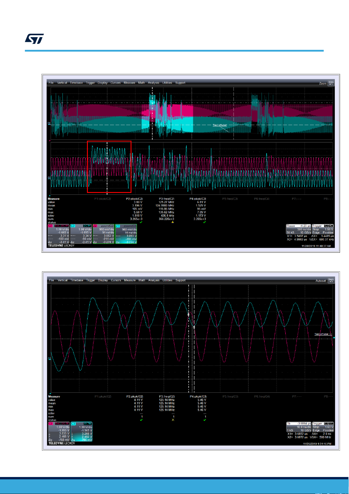
Note: at 125 MHz as RGMII clock at 1 giga, the period is 8 ns.
Figure 7. PLL_ETH with XOSC selection and DoS enable
TN1337
Giga measurements
The figures below report the measurements of the delay showing that there is the shift of 90 degrees (2ns) as
expected that guarantees the working connectivity at 1 GiGa speed. Same result has been obtained when use, as
PLL_ETH source, the PLL0 instead of the XOSC.
Note: in the figures below the purple line is the Channel #2 for TX_CLK. insetead the TXDATA[0] is the blue channel
#3.
TN1337 - Rev 1
page 10/19
Page 11
PLL_ETH with XOSC selection and DoS
Figure 8. 1GiGa: PLL_ETH sourced by XOSC - Oscilloscope view
TN1337
Figure 9. 1GiGa: DoS 2ns delay - PLL_ETH sourced by XOSC
TN1337 - Rev 1
page 11/19
Page 12

7 100 Mbps measurements
The following cases aim to detail the impact of DoS on 100 Mbps. For this speed, the extra delay on TX_CLK is
not mandatory, in fact the PHY low level driver is programmed not to add any delay. It has been noted that when
using DoS and DoD configuration the network activity is not affected (it is able to exchange data from the card to
the remote partner) and data and clock are perfectly aligned.
7.1 PLL_ETH with XOSC selection and DoS
Figure 10. 100Mbps: PLL_ETH - XOSC selection with DoS enable
TN1337
100 Mbps measurements
TN1337 - Rev 1
page 12/19
Page 13

7.2 TX_CLK from RX_CLK (DoD)
The following figure shows that the TX_CLK is selected from the transceiver and DoS is disabled.
Figure 11. TX_CLK from RX_CLK – no delay
TN1337
TX_CLK from RX_CLK (DoD)
Figure 12. 100Mbps: TX_CLK with DoD
TN1337 - Rev 1
page 13/19
Page 14

TN1337
Conclusions
8 Conclusions
This technical note provides some details on how to manage skew.There are three main approaches:
• The transceiver has its own extended register set to add skew to signals.
• The PCB can be modified to have a trace routing for the TX_CLK.
• The micro-controller can introduce the delay.
As a general rule, the calculation of the necessary skew and delay correction must be analyzed case by case
following the RGMII specification and the technical data sheet of the devices. Further measurements on the PCB
can help to understand the necessary signal delay. To provide adequate flexibility and leeway to fine tune skew
you can have the DoS function on the microcontroller as well as a transceiver capable of introducing additional
delay.
The main focus is the SPC58EHx / SPC58NHx DoS functionality. It has been shown that the expected delay
is introduced during the DoS configuration and the whole network connectivity is working at different speeds
removing any dependence on the transceiver and PCB.
Note: Microchip KSZ9031RNX can add further misalignment on the signals by programming the internal registers.
Note: a phisycal device can implement signal delays internally also via HW belt option.
TN1337 - Rev 1
page 14/19
Page 15

TN1337
Network setup
Appendix A Network setup
SPC5Studio's high-level application, based on the operating system and TCP / IP network stacks, is configured to
have full network protocols running, for example ICMP, ARP, UDP, TCP.
Below is the configuration used to check if the network works (for example Ping command to target from a remote
host).
Figure 13. Ethernet_1 external connection
A.1 Acronyms and abbreviations
Abbreviation Complete name
MAC Medium Access Control
DoS Delay on Source
DoD Delay on Destination
RGMII Reduced gigabit media independent interface
ICMP Internet Control Message Protocol
ARP Address Resolution Protocol
UDP User Datagram Protocol
TCP Transmission Control Protocol
Skew Delay between clock and data transitions
PCB Printed Circuit Board
A.2 Reference documents
• RM0452 Reference manual.
• SPC58EHx, SPC58NHx datasheet.
• TN1257 SPC58EHx, SPC58NHx IO definition: signal description and input multiplexing tables.
• Microchip SZ9031RNX (DS00002117F).
• RGMII/RTBI specification version 2.6 from HP/Marvell.
• OPEN Alliance RGMII EPL (Electrical-Physical Layer) Recommendations for automotive.
Table 1. Acronyms
TN1337 - Rev 1
page 15/19
Page 16
Revision history
TN1337
Table 2. Document revision history
Date Version Changes
18-Jan-2021 1 Initial release.
TN1337 - Rev 1
page 16/19
Page 17

TN1337
Contents
Contents
1 RGMII overview....................................................................2
1.1 RGMII timing specification .......................................................2
2 SPC58EHx/SPC58NHx RGMII clocking schema .....................................4
2.1 TX_CLK selection with Delay on Source (DoS) .....................................4
2.2 TX_CLK selection with Delay on Destination (DoD) ..................................4
3 Microchip KSZ9031RNX RGMII transceiver .........................................5
3.1 GTX_CLK delay from transceiver registers .........................................5
3.2 PCB trace routing on GTX_CLK ..................................................6
4 Hardware ..........................................................................7
5 SPC58EHx/SPC58NHx TX_CLK programming ......................................9
6 Giga measurements ..............................................................10
6.1 PLL_ETH with XOSC selection and DoS ..........................................10
7 100 Mbps measurements .........................................................12
7.1 PLL_ETH with XOSC selection and DoS ..........................................12
7.2 TX_CLK from RX_CLK (DoD) ...................................................13
8 Conclusions ......................................................................14
Appendix A Network setup ...........................................................15
A.1 Acronyms and abbreviations ....................................................15
A.2 Reference documents..........................................................15
Revision history .......................................................................16
Contents ..............................................................................17
List of figures..........................................................................18
TN1337 - Rev 1
page 17/19
Page 18

TN1337
List of figures
List of figures
Figure 1. RGMII RX timing diagram ............................................................ 2
Figure 2. RGMII TX Timing diagram ............................................................3
Figure 3. SPC58EHx RGMII clock schema .......................................................4
Figure 4. PCB trace routing on GTX_CLK ........................................................6
Figure 5. SPC58NHADPT302S connections ......................................................7
Figure 6. SPC58NHADPT302S - KSZ9031NX schematic (and test points).................................. 8
Figure 7. PLL_ETH with XOSC selection and DoS enable ............................................10
Figure 8. 1GiGa: PLL_ETH sourced by XOSC - Oscilloscope view ...................................... 11
Figure 9. 1GiGa: DoS 2ns delay - PLL_ETH sourced by XOSC ........................................ 11
Figure 10. 100Mbps: PLL_ETH - XOSC selection with DoS enable....................................... 12
Figure 11. TX_CLK from RX_CLK – no delay ..................................................... 13
Figure 12. 100Mbps: TX_CLK with DoD .........................................................13
Figure 13. Ethernet_1 external connection........................................................ 15
TN1337 - Rev 1
page 18/19
Page 19

TN1337
IMPORTANT NOTICE – PLEASE READ CAREFULLY
STMicroelectronics NV and its subsidiaries (“ST”) reserve the right to make changes, corrections, enhancements, modifications, and improvements to ST
products and/or to this document at any time without notice. Purchasers should obtain the latest relevant information on ST products before placing orders. ST
products are sold pursuant to ST’s terms and conditions of sale in place at the time of order acknowledgement.
Purchasers are solely responsible for the choice, selection, and use of ST products and ST assumes no liability for application assistance or the design of
Purchasers’ products.
No license, express or implied, to any intellectual property right is granted by ST herein.
Resale of ST products with provisions different from the information set forth herein shall void any warranty granted by ST for such product.
ST and the ST logo are trademarks of ST. For additional information about ST trademarks, please refer to www.st.com/trademarks. All other product or service
names are the property of their respective owners.
Information in this document supersedes and replaces information previously supplied in any prior versions of this document.
© 2021 STMicroelectronics – All rights reserved
TN1337 - Rev 1
page 19/19
 Loading...