

TN1215, TS1220
TYN612, TYN812, TYN1012
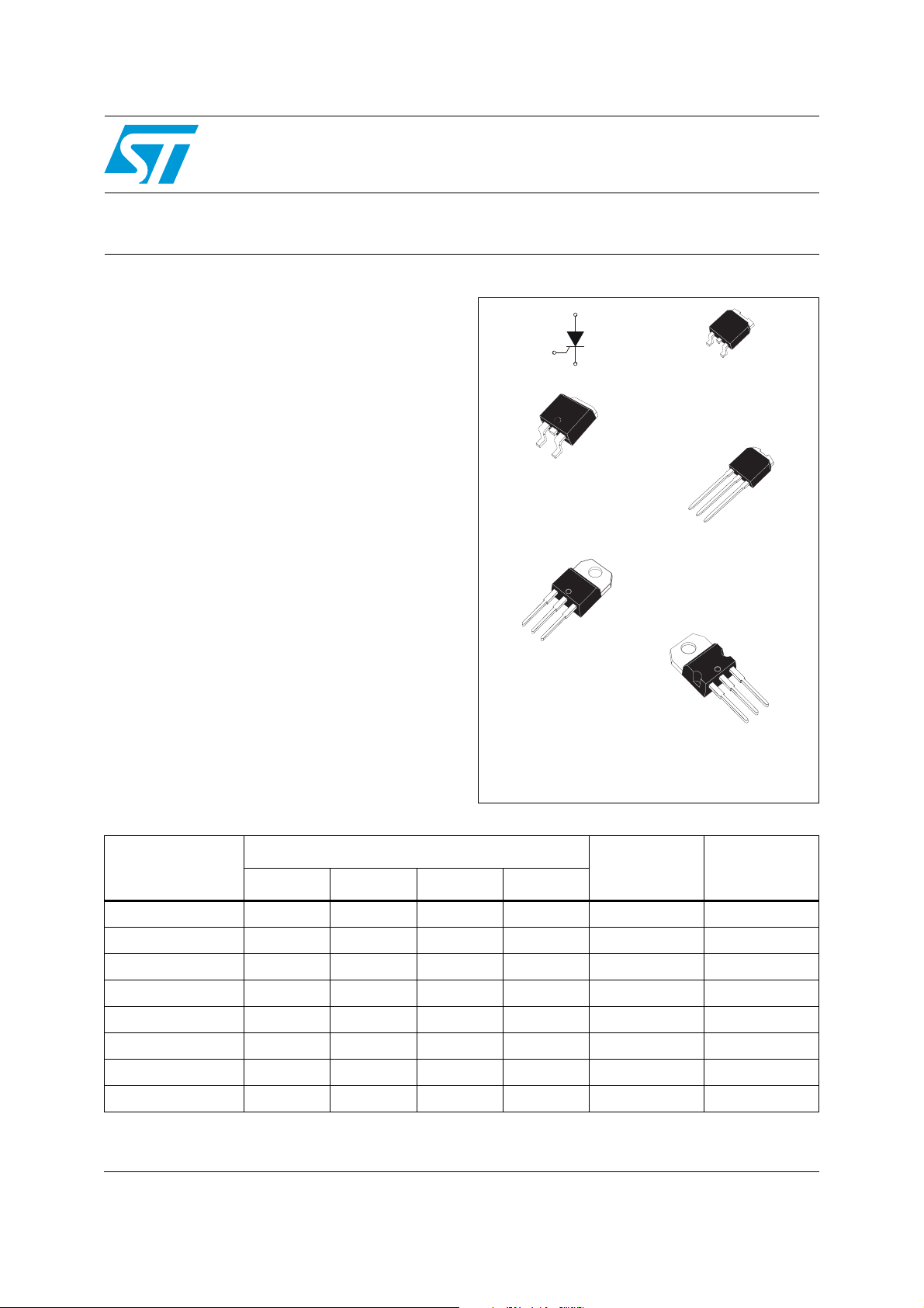
Sensitive and standard 12 A SCRs
Features
■ On-state rms current, I
■ Repetitive peak off-state voltage, V
600 to 1000 V
■ Triggering gate current, I
T(RMS)
0.2 to 15 mA
GT
12 A
DRM/VRRM
Description
Available either in sensitive (TS1220) or standard
(TN1215 / TYNx12) gate triggering levels, the
12 A SCR series is suitable to fit all modes of
control, found in applications such as overvoltage
crowbar protection, motor control circuits in power
tools and kitchen aids, inrush current limiting
circuits, capacitive discharge ignition and voltage
regulation circuits.
Available in through-hole or surface-mount
packages, they provide an optimized performance
in a limited space area.
A
G
K
A
TN1215-xxxB
K
A
G
DPAK
A
TS1220-xxxB
K
A
G
2
PAK
D
A
TN1215-xxxG
TS1220-xxxG
A
K
A
G
IPAK
TN1215-xxxH
TS1220-xxxH
K
A
G
A
TO-220AB
TYNx12RG
TYNx12TRG
G
A
K
TO-220AB
TS1220-xxxT
Table 1. Device summary
Voltage (xxx) V
Order code
600 V 700 V 800 V 1000 V
DRM/VRRM
Sensitivity
IGT
Package
TN1215-xxxB X X 15 mA DPAK
TN1215-xxxG X X 15 mA D
2
PA K
TN1215-xxxH X X 15 mA IPAK
TS1220-xxxB X X 0.2 mA DPAK
TS1220-xxxH X 0.2 mA IPAK
TS1220-xxxT X 0.2 mA TO-220AB
TYNx12RG X X X 15 mA TO-220AB
TYNx12TRG X X X 5 mA TO-220AB
September 2011 Doc ID 7475 Rev 7 1/13
www.st.com
13
Characteristics TN1215, TS1220, TYN612, TYN812, TYN1012
1 Characteristics
Table 2. Absolute ratings (limiting values)
Value
Symbol Parameter
TN1215-G
TYNx12
TN1215-B/-H
TS1220-B/-H/T
Unit
I
T(RMS)
I
T(AV)
I
TSM
dI/dt
I
GM
P
G(AV)
T
V
RGM
Table 3. Sensitive electrical characteristics (Tj = 25 °C, unless otherwise specified)
RMS on-state current (180 °Conduction angle) Tc = 105 °C 12 A
Average on-state current (180 °Conduction angle) Tc = 105 °C 8 A
Non repetitive surge peak on-state
current
²
²
tI
I
t Value for fusing tp = 10 ms Tj = 25 °C 98 60 A
Critical rate of rise of on-state
current I
= 2 x IGT, tr ≤ 100 ns
G
= 8.3 ms
t
p
= 10 ms 140 110
t
p
F = 60 Hz T
= 25 °C
T
j
= 125 °C 50 A/µs
j
145 115
Peak gate current tp = 20 µs Tj = 125 °C 4 A
Average gate power dissipation Tj = 125 °C 1 W
Storage junction temperature range
stg
T
Operating junction temperature range
j
Maximum peak reverse gate voltage
(for TN1215 and TYNx12 only)
- 40 to + 150
- 40 to + 125
5V
Symbol Test conditions TS1220 Unit
I
GT
V
GT
V
GD
V
RGIRG
I
H
I
L
dV/dt V
V
TM
V
t0
R
d
I
DRM
I
RRM
VD = 12 V, RL = 140 Ω
VD = V
DRM, RL
= 3.3 kΩ, RGK = 220 Ω Tj = 125 °C MIN. 0.1 V
= 10 µA MIN. 8 V
IT = 50 mA, RGK = 1 kΩ MAX. 5 mA
IG = 1 mA, RGK = 1 kΩ MAX. 6 mA
= 65 % V
D
DRM, RGK
= 220 Ω Tj = 125 °C MIN. 5 V/µs
ITM = 24 A, tp = 380 µs Tj = 25 °C MAX. 1.6 V
Threshold voltage Tj = 125 °C MAX. 0.85 V
Dynamic resistance Tj = 125 °C MAX. 30 mΩ
T
= 25 °C
V
DRM
= V
, RGK = 220 Ω
RRM
j
= 125 °C 2 mA
T
j
MAX. 200 µA
MAX. 0.8 V
5µA
MAX.
A
°C
2
S
2/13 Doc ID 7475 Rev 7
TN1215, TS1220, TYN612, TYN812, TYN1012 Characteristics
Table 4. Standard electrical characteristics (Tj = 25 °C, unless otherwise specified)
TN1215 TYN
Symbol Test conditions
B / H G x12T x12
Unit
I
GT
V
V
I
dV/dt V
V
V
R
I
DRM
I
RRM
Table 5. Thermal resistance
VD = 12 V RL = 33 Ω
GT
VD = V
GD
IT = 500 mA Gate open MAX. 40 30 15 30 mA
H
IG = 1.2 I
I
L
= 67 % V
D
ITM = 24 A tp = 380 µs Tj = 25 °C MAX. 1.6 V
TM
Threshold voltage Tj = 125 °C MAX. 0.85 V
t0
Dynamic resistance Tj = 125 °C MAX. 30 mΩ
d
RL = 3.3 kΩ Tj = 125 °C MIN. 0.2 V
DRM
GT
Gate open Tj =125 °C MIN. 200 40 200 V/µs
DRM
Tj = 25 °C
V
= V
DRM
RRM
T
= 125 °C 2 mA
j
MAX. 15 5 15
MAX. 1.3 V
MAX. 80 60 30 60 mA
5µA
MAX.
Symbol Parameter Value Unit
MIN. 2 0.5 2
R
R
th(j-c)
th(j-a)
Junction to case (DC) 1.3 °C/W
(1)
= 0.5 cm²DPAK 70
S
(1)
S
= 1 cm²D2PA K 4 5
Junction to ambient (DC)
IPAK 100
mA
°C/W
1. S = Copper surface under tab
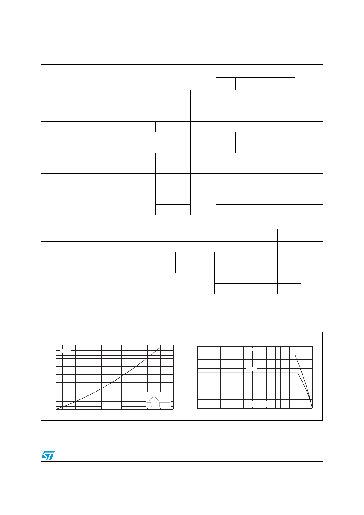
Figure 1. Maximum average power
dissipation versus average
on-state current
P(W)
12
11
α = 180°
10
9
8
7
6
5
4
3
2
1
0
0123456789
I (A)
T(AV)
TO-220AB 60
Figure 2. Average and DC on-state current
versus case temperature
I (A)
T(AV)
14
12
10
8
6
360°
α
4
2
0
0 25 50 75 100 125
Doc ID 7475 Rev 7 3/13
D.C.
α = 180°
T (°C)
case
Characteristics TN1215, TS1220, TYN612, TYN812, TYN1012
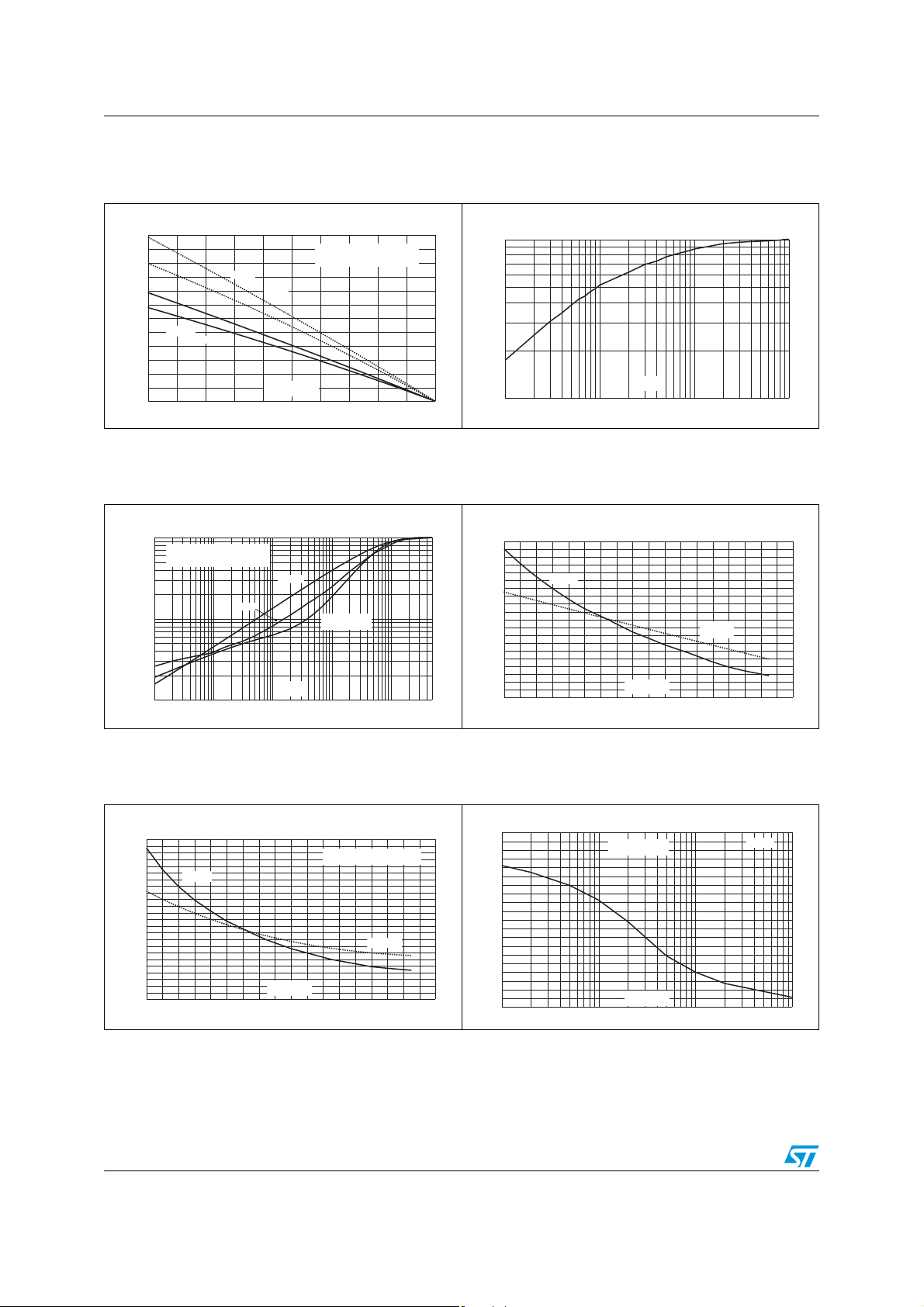
Figure 3. Average and D.C. on-state current
versus ambient temperature
(DPAK)
I (A)
T(AV)
3.0
Device mounted on FR4 with
2.5
2.0
1.5
α = 180°
1.0
0.5
0.0
0 25 50 75 100 125
D.C.
2
DPAK
DPAK
T (°C)
recommended pad layout
amb
Figure 5. Relative variation of thermal
impedance junction to ambient
versus pulse duration (DPAK)
K=[Z /R
1.00
0.10
0.01
th(j-a) th(j-a)
Device mounted on FR4 with
recommended pad layout
1E-2 1E-1 1E+0 1E+1 1E+2 5E+2
]
2
DPAK
DPAK
t (s)
p
TO-220AB / IPAK
Figure 4. Relative variation of thermal
impedance junction to case versus
pulse duration
K=[Z /R
th(j-c) th(j-c)
1.0
0.5
0.2
0.1
1E-3 1E-2 1E-1 1E+0
]
t (s)
p
Figure 6. Relative variation of gate trigger
and holding current versus junction
temperature for TS1220 series
I,I,I[T] /
GTHL j
2.0
1.8
1.6
1.4
1.2
1.0
0.8
0.6
0.4
0.2
0.0
-40 -20 0 20 40 60 80 100 120 140
I ,I ,I [T =25°C]
GT H L j
I
GT
T (°C)
j
IH& I
R = 1k
GK
L
Ω
Figure 7. Relative variation of gate trigger
Figure 8. Relative variation of holding
and holding current versus junction
temperature
I [R ] / I [ =1k ]
I,I,I[T] /
GTHL j
2.4
2.2
2.0
1.8
1.6
1.4
1.2
1.0
0.8
0.6
0.4
0.2
0.0
-40 -20 0 20 40 60 80 100 120 140
I ,I ,I [T =25°C]
GTHL j
I
GT
T (°C)
j
TN1215 and TYNx12 Series
IH& I
L
4/13 Doc ID 7475 Rev 7
HGK HΩRGK
5.0
4.5
4.0
3.5
3.0
2.5
2.0
1.5
1.0
0.5
0.0
1E-2 1E-1 1E+0 1E+1
current versus gate-cathode
resistance (typical values)
TS1220 Series
R(k)GKΩ
Tj= 25°C

TN1215, TS1220, TYN612, TYN812, TYN1012 Characteristics
Figure 9. Relative variation of dV/dt immunity
versus gate-cathode resistance
(typical values) for TS12 series
dV/dt[R ] / dV/dt[ =220 ]
10.0
1.0
0.1
GK
0 200 400 600 800 1000 1200
GK
ΩR
R(k)GKΩ
Tj= 125°C
V = 0.67 x V
D DRM
Figure 11. Surge peak on-state current versus
number of cycles
I (A)
TSM
150
140
130
120
110
100
90
80
70
60
50
40
30
20
10
0
1 10 100 1000
TS12
Repetitive
T =105°C
C
TN12 / TYN12
Non repetitive
T initial=25°C
j
Number of cycles
t =10ms
p
One cycle
Figure 10. Relative variation of dV/dt immunity
versus gate-cathode capacitance
(typical values) for TS12 series
dV/dt[C ] / dV/dt[ =220 ]GKΩR
4.0
V = 0.67 x V
D DRM
T
= 125°C
j
3.5
3.0
2.5
2.0
1.5
1.0
0.5
0.0
0 25 50 75 100 125 150
R = 220
GK
Ω
GK
C (nF)
GK
Figure 12. Non-repetitive surge peak on-state
current and corresponding values
of I²t versus sinusoidal pulse width
22
I (A), I t (A s)
TSM
2000
I
1000
dI/dt limitation
100
10
0.01 0.10 1.00 10.00
TSM
t (ms)
p
TS12
2
I t
TN12 / TYN12
TN12 / TYN12
T initial = 25°C
j
TS12
Figure 13. On-state characteristics (maximum
values)
I (A)
TM
200
T max.:
j
V =0.85V
100
t0
R =30m
Ω
d
Tj=max
10
1
0.0 0.5 1.0 1.5 2.0 2.5 3.0 3.5 4.0 4.5 5.0
T =25°C
j
V (V)
TM
Doc ID 7475 Rev 7 5/13
Figure 14. Thermal resistance junction to
ambient versus copper surface
under tab (DPAK and D
R (°C/W)
th(j-a)
100
Epoxy printed circuit board FR4
80
60
40
20
0
02468101214161820
2
DPAK
DPAK
copper thickness = 35 µm
S(cm²)
2
PAK )

Ordering information scheme TN1215, TS1220, TYN612, TYN812, TYN1012
2 Ordering information scheme
Figure 15. TN1215 series
TN 12 15 - 600 B (-TR)
Standard SCR series
Current
12 = 12 A
Sensitivity
15 = 15 mA
Voltage
600 = 600 V
800 = 800 V
Packag e
B = DPAK
2
G = D PAK
H = IPAK
Packing mode
Blank = Tube
-TR = Tape and reel (DPAK and
Figure 16. TS1220 series
2
D PAK)
TS 12 20 - 600 B (-TR)
Sensitive SCR series
Current
12 = 12 A
Sensitivity
20 = 200 µA
Voltage
600 = 600 V
700 = 700 V
Packag e
B = DPAK
H = IPAK
T = TO-220AB
Packing mode
Blank = Tube
-TR = Tape and reel
Figure 17. TYNx12 series
Standard SCR series
Voltage
6 = 600 V
8 = 800 V
10 = 1000 V
Current
12 = 12 A
Sensitivity
Blank = 15 mA
T = 5 mA
Packing mode
RG = Tube
TYN 6 12 T RG
6/13 Doc ID 7475 Rev 7

TN1215, TS1220, TYN612, TYN812, TYN1012 Package information
3 Package information
● Epoxy meets UL94, V0
● Lead-free packages
In order to meet environmental requirements, ST offers these devices in different grades of
ECOPACK
specifications, grade definitions and product status are available at: www.st.com.
ECOPACK
Table 6. TO-220AB dimensions (devices TYNx12RG and TYNx12TRG)
®
packages, depending on their level of environmental compliance. ECOPACK®
®
is an ST trademark.
Dimensions
Ref.
Millimeters Inches
Min. Typ. Max. Min. Typ. Max.
A 15.20 15.90 0.598 0.625
B
Ø I
L
A
I4
l3
a1
l2
a2
C
b2
c2
a1 3.75 0.147
a2 13.00 14.00 0.511 0.551
B 10.00 10.40 0.393 0.409
F
b1 0.61 0.88 0.024 0.034
b2 1.23 1.32 0.048 0.051
C 4.40 4.60 0.173 0.181
c1 0.49 0.70 0.019 0.027
c2 2.40 2.72 0.094 0.107
e 2.40 2.70 0.094 0.106
F 6.20 6.60 0.244 0.259
M
c1
b1
e
ØI 3.75 3.85 0.147 0.151
I4 15.80 16.40 16.80 0.622 0.646 0.661
L 2.65 2.95 0.104 0.116
l2 1.14 1.70 0.044 0.066
l3 1.14 1.70 0.044 0.066
M2.60 0.102
Doc ID 7475 Rev 7 7/13

Package information TN1215, TS1220, TYN612, TYN812, TYN1012
Table 7. TO-220AB dimensions (device TS1220-xxxT)
Dimensions
L2
F2
F1
F
G1
H2
Dia
G
L5
L9
L6
L4
Ref.
Millimeters Inches
Min. Max. Min. Max.
A 4.40 4.60 0.173 0.181
C 1.23 1.32 0.048 0.051
A
C
D 2.40 2.72 0.094 0.107
E 0.49 0.70 0.019 0.027
L7
F 0.61 0.88 0.024 0.034
F1 1.14 1.70 0.044 0.066
F2 1.14 1.70 0.044 0.066
G 4.95 5.15 0.194 0.202
D
G1 2.40 2.70 0.094 0.106
H2 10 10.40 0.393 0.409
L2 16.4 typ. 0.645 typ.
M
E
L4 13 14 0.511 0.551
L5 2.65 2.95 0.104 0.116
L6 15.25 15.75 0.600 0.620
L7 6.20 6.60 0.244 0.259
L9 3.50 3.93 0.137 0.154
M 2.6 typ. 0.102 typ.
8/13 Doc ID 7475 Rev 7
Diam. 3.75 3.85 0.147 0.151

TN1215, TS1220, TYN612, TYN812, TYN1012 Package information
Table 8. IPAK dimensions
Dimensions
Ref.
Millimeters Inches
Min. Typ. Max. Min. Typ. Max.
A 2.20 2.40 0.086 0.094
A1 0.90 1.10 0.035 0.043
A3 0.70 1.30 0.027 0.051
A
E
B2
L2
C2
B 0.64 0.90 0.025 0.035
B2 5.20 5.40 0.204 0.212
B3 0.95 0.037
B5 0.30 0.035
D
C 0.45 0.60 0.017 0.023
C2 0.48 0.60 0.019 0.023
H
L1
L
B3
B
V1
A1
D 6 6.20 0.236 0.244
E 6.40 6.60 0.252 0.260
e2.28 0.090
B5
e
G
C
A3
G 4.40 4.60 0.173 0.181
H 16.10 0.634
L 9 9.40 0.354 0.370
L1 0.8 1.20 0.031 0.047
L2 0.80 1 0.031 0.039
V1 10° 10°
Doc ID 7475 Rev 7 9/13

Package information TN1215, TS1220, TYN612, TYN812, TYN1012
Table 9. DPAK dimensions
Dimensions
Ref.
Min. Max. Min. Max.
A 2.20 2.40 0.086 0.094
E
B2
L2
H
L4
B
G
A1
A
C2
R
D
R
C
A1 0.90 1.10 0.035 0.043
A2 0.03 0.23 0.001 0.009
B 0.64 0.90 0.025 0.035
B2 5.20 5.40 0.204 0.212
C 0.45 0.60 0.017 0.023
C2 0.48 0.60 0.018 0.023
D 6.00 6.20 0.236 0.244
E 6.40 6.60 0.251 0.259
0.60 MIN.
A2
G 4.40 4.60 0.173 0.181
H 9.35 10.10 0.368 0.397
V2
L2 0.80 typ. 0.031 typ.
L4 0.60 1.00 0.023 0.039
V2 0° 8° 0° 8°
Figure 18. DPAK footprint dimensions (in millimeters)
Millimeters Inches
6.7
6.7 3 3
1.6
2.3
2.3
1.6
10/13 Doc ID 7475 Rev 7

TN1215, TS1220, TYN612, TYN812, TYN1012 Package information
D
Table 10. D
L2
L
L3
2
PAK dimensions
E
A1
B2
B
G
2mm min.
FLAT ZONE
Dimensions
Ref.
Millimeters Inches
Min. Typ. Max. Min. Typ. Max.
A 4.30 4.60 0.169 0.181
A
C2
A1 2.49 2.69 0.098 0.106
A2 0.03 0.23 0.001 0.009
B 0.70 0.93 0.027 0.037
B2 1.25 1.40 0.048 0.055
C 0.45 0.60 0.017 0.024
C2 1.21 1.36 0.047 0.054
C
R
D 8.95 9.35 0.352 0.368
E 10.00 10.28 0.393 0.405
A2
G 4.88 5.28 0.192 0.208
L 15.00 15.85 0.590 0.624
V2
L2 1.27 1.40 0.050 0.055
L3 1.40 1.75 0.055 0.069
R 0.40 0.016
V2 0° 8° 0° 8°
Figure 19. D2PAK footprint dimensions (in millimeters)
16.90
10.30
1.30
8.90
3.70
5.08
Doc ID 7475 Rev 7 11/13

Ordering information TN1215, TS1220, TYN612, TYN812, TYN1012
4 Ordering information
Table 11. Ordering information
Order code
(1)
Marking
TN1215-x00B TN12 15x00 DPAK 0.3 g 75 Tube
TN1215-x00B-TR TN12 15x00 DPAK 0.3 g 2500 Tape and reel
TN1215-x00G TN1215x00G D
TN1215-x00G-TR TN1215x00G D
TN1215-x00H TN12 15x00 IPAK 0.3 g 75 Tube
TS1220-x00B TS12 20x00 DPAK 0.3 g 75 Tube
TS1220-x00B-TR TS12 20x00 DPAK 0.3 g 2500 Tape and reel
TS1220-x00H TS12 20x00 IPAK 0.3 g 75 Tube
TS1220-x00T TS1220600T TO-220AB 2.3 g 50 Tube
TYNx12RG TYNx12 TO-220AB 2.3 g 50 Tube
TYNx12TRG TYNx12T TO-220AB 2.3 g 50 Tube
1. x (6, 7, 8, 10) depends upon voltage
(1)
Package Weight Base qty Delivery mode
2
PAK 1.5 g 50 Tube
2
PAK 1.5 g 1000 Tape and reel
5 Revision history
Table 12. Document revision history
Date Revision Changes
Sep-2000 3 Last update.
25-Mar-2005 4 TO-220AB delivery mode changed from bulk to tube.
14-Oct-2005 5
08-Mar-2007 6
12-Oct-2009 7 Added TS1220-xxxT device.
Changed sensitivity values in Ta bl e 1 for TYNx12 (30 to 15 mA) and
TYNx12T ( 15 to 5 mA). Added ECOPACK statement.
Reformatted to current standard.
Figure 15: TN1215 series product name corrected.
Figure 16: TS1220 series product name corrected.
12/13 Doc ID 7475 Rev 7

TN1215, TS1220, TYN612, TYN812, TYN1012
Please Read Carefully:
Information in this document is provided solely in connection with ST products. STMicroelectronics NV and its subsidiaries (“ST”) reserve the
right to make changes, corrections, modifications or improvements, to this document, and the products and services described herein at any
time, without notice.
All ST products are sold pursuant to ST’s terms and conditions of sale.
Purchasers are solely responsible for the choice, selection and use of the ST products and services described herein, and ST assumes no
liability whatsoever relating to the choice, selection or use of the ST products and services described herein.
No license, express or implied, by estoppel or otherwise, to any intellectual property rights is granted under this document. If any part of this
document refers to any third party products or services it shall not be deemed a license grant by ST for the use of such third party products
or services, or any intellectual property contained therein or considered as a warranty covering the use in any manner whatsoever of such
third party products or services or any intellectual property contained therein.
UNLESS OTHERWISE SET FORTH IN ST’S TERMS AND CONDITIONS OF SALE ST DISCLAIMS ANY EXPRESS OR IMPLIED
WARRANTY WITH RESPECT TO THE USE AND/OR SALE OF ST PRODUCTS INCLUDING WITHOUT LIMITATION IMPLIED
WARRANTIES OF MERCHANTABILITY, FITNESS FOR A PARTICULAR PURPOSE (AND THEIR EQUIVALENTS UNDER THE LAWS
OF ANY JURISDICTION), OR INFRINGEMENT OF ANY PATENT, COPYRIGHT OR OTHER INTELLECTUAL PROPERTY RIGHT.
UNLESS EXPRESSLY APPROVED IN WRITING BY TWO AUTHORIZED ST REPRESENTATIVES, ST PRODUCTS ARE NOT
RECOMMENDED, AUTHORIZED OR WARRANTED FOR USE IN MILITARY, AIR CRAFT, SPACE, LIFE SAVING, OR LIFE SUSTAINING
APPLICATIONS, NOR IN PRODUCTS OR SYSTEMS WHERE FAILURE OR MALFUNCTION MAY RESULT IN PERSONAL INJURY,
DEATH, OR SEVERE PROPERTY OR ENVIRONMENTAL DAMAGE. ST PRODUCTS WHICH ARE NOT SPECIFIED AS "AUTOMOTIVE
GRADE" MAY ONLY BE USED IN AUTOMOTIVE APPLICATIONS AT USER’S OWN RISK.
Resale of ST products with provisions different from the statements and/or technical features set forth in this document shall immediately void
any warranty granted by ST for the ST product or service described herein and shall not create or extend in any manner whatsoever, any
liability of ST.
ST and the ST logo are trademarks or registered trademarks of ST in various countries.
Information in this document supersedes and replaces all information previously supplied.
The ST logo is a registered trademark of STMicroelectronics. All other names are the property of their respective owners.
© 2011 STMicroelectronics - All rights reserved
STMicroelectronics group of companies
Australia - Belgium - Brazil - Canada - China - Czech Republic - Finland - France - Germany - Hong Kong - India - Israel - Italy - Japan -
Malaysia - Malta - Morocco - Philippines - Singapore - Spain - Sweden - Switzerland - United Kingdom - United States of America
www.st.com
Doc ID 7475 Rev 7 13/13
 Loading...