

Features
VFQFPN2-48
■ Single-chip solution for ISM 2.45 GHz RF
transceiver
■ Built-in ranging capability for link distance
estimation
■ Modulation technique: chirp spread spectrum
(CSS)
■ FDMA support: 7 channels, 3 non-overlapping
■ Data rates: 2 and 1 Mbps; 500, 250 and 125
kbps
■ Adjustable output power from -33 dBm to
0dBm
■ Receiver sensitivity: -97 dBm @ 250 kbps,
FEC, and BER=10-3
■ In-band carrier-to-interference C/I = 0 to 3 dB
@ 250 kbps & C=-80 dBm
■ Supports external power amplifier to increase
output power
■ High precision ranging: 2 m indoors and 1 m
outdoors
■ Supply voltage range from 2.3 V to 2.7 V
■ Current consumption: 27 mA (RX), 30 mA (TX)
@ 0 dBm
■ Standby current with active RTC: 2 µA
■ RSSI sensitivity: -95 dBm
■ 32.768 kHz clock available for external MCU
■ Integrated fast SPI interface (27 Mbps)
■ Integrated MAC controller with FEC, CRC
checking
■ CSMA/CA, FDMA, and TDMA modes
■ Automatic retransmission and
acknowledgement
■ Automatic address matching
■ Industrial temperature range from -40°C to
+85°C
■ VFQFPN2-48 ECOPACK® package
TN100
High performance CSS transceiver
enabling location awareness
Preliminary Data
Description
The TN100 transceiver is a highly integrated
mixed signal chip that uses the wireless
communication technology CSS (chirp spread
spectrum) developed by Nanotron Technologies.
With its unique ranging capability, TN100 can
measure the link distance between two nodes.
Thus, TN100 supports location awareness
applications including location based services
(LBS) and asset tracking (2D/3D RTLS). Ranging
is performed during regular data communication
and does not require additional infrastructure,
power, and/or bandwidth.
For an even better ranging accuracy, a high
precision mode is provided. SDS-TWR algorithm
(symmetrical double-sided two-way ranging)
allows superior accuracy even with the use of low
cost crystals for the oscillators.
September 2008 Rev 1 1/235
This is preliminary information on a new product now in development or undergoing evaluation. Details are subject to
change without notice.
www.st.com
1

Contents TN100
Contents
1 Summary description . . . . . . . . . . . . . . . . . . . . . . . . . . . . . . . . . . . . . . . 13
2 TN100 block diagram . . . . . . . . . . . . . . . . . . . . . . . . . . . . . . . . . . . . . . . 14
3 Key features . . . . . . . . . . . . . . . . . . . . . . . . . . . . . . . . . . . . . . . . . . . . . . . 15
3.1 Built-in ranging capability . . . . . . . . . . . . . . . . . . . . . . . . . . . . . . . . . . . . . 15
3.2 Channelization using FDMA for improved coexistence . . . . . . . . . . . . . . 15
3.3 Incorporated digital dispersive delay-line (DDDL) . . . . . . . . . . . . . . . . . . 15
3.4 Selectable symbol durations and symbol rates . . . . . . . . . . . . . . . . . . . . 15
4 Architecture . . . . . . . . . . . . . . . . . . . . . . . . . . . . . . . . . . . . . . . . . . . . . . . 16
4.1 Analog part - TX and RX . . . . . . . . . . . . . . . . . . . . . . . . . . . . . . . . . . . . . 16
4.2 Digital part - programming interface . . . . . . . . . . . . . . . . . . . . . . . . . . . . . 16
4.2.1 Digital part – ON Section . . . . . . . . . . . . . . . . . . . . . . . . . . . . . . . . . . . . 16
4.2.2 Digital part – PWD section . . . . . . . . . . . . . . . . . . . . . . . . . . . . . . . . . . . 16
4.3 Signal flow . . . . . . . . . . . . . . . . . . . . . . . . . . . . . . . . . . . . . . . . . . . . . . . . 17
4.4 Commonly used set of register default values . . . . . . . . . . . . . . . . . . . . . 17
4.5 Programmable pull-resistors . . . . . . . . . . . . . . . . . . . . . . . . . . . . . . . . . . 17
5 Pin description . . . . . . . . . . . . . . . . . . . . . . . . . . . . . . . . . . . . . . . . . . . . 18
5.1 Input and/or output pins . . . . . . . . . . . . . . . . . . . . . . . . . . . . . . . . . . . . . . 20
5.2 Configuring the digital I/O pins – D0 to D3 (pins 19 to 22) . . . . . . . . . . . . 21
5.3 Configuring the IRQ Pin – µCIRQ (pin 27) . . . . . . . . . . . . . . . . . . . . . . . . 22
5.4 Power-on reset – /POnReset (pin 30) . . . . . . . . . . . . . . . . . . . . . . . . . . . 22
6 Memory map . . . . . . . . . . . . . . . . . . . . . . . . . . . . . . . . . . . . . . . . . . . . . . 23
6.1 Selecting a memory address . . . . . . . . . . . . . . . . . . . . . . . . . . . . . . . . . . 24
6.2 128-byte programmable register block . . . . . . . . . . . . . . . . . . . . . . . . . . . 25
6.2.1 Accessing a register address location . . . . . . . . . . . . . . . . . . . . . . . . . . 25
6.2.2 Setting a shadow variable for the RAM access register . . . . . . . . . . . . . 26
6.3 Correlator RAM access . . . . . . . . . . . . . . . . . . . . . . . . . . . . . . . . . . . . . . 26
6.4 Chirp sequencer RAM access . . . . . . . . . . . . . . . . . . . . . . . . . . . . . . . . . 26
2/235

TN100 Contents
7 Clocking structure . . . . . . . . . . . . . . . . . . . . . . . . . . . . . . . . . . . . . . . . . . 27
7.1 Overview . . . . . . . . . . . . . . . . . . . . . . . . . . . . . . . . . . . . . . . . . . . . . . . . . 27
7.2 32.786 kHz real-time clock (RTC) . . . . . . . . . . . . . . . . . . . . . . . . . . . . . . 27
7.2.1 Updating and reading the RTC through software . . . . . . . . . . . . . . . . . 28
7.2.2 Manually or automatically updating the RTC using TimeB packets . . . . 29
7.2.3 Using the RTC as wake-up event . . . . . . . . . . . . . . . . . . . . . . . . . . . . . 30
7.3 SPI clock . . . . . . . . . . . . . . . . . . . . . . . . . . . . . . . . . . . . . . . . . . . . . . . . . 30
7.4 32-MHz baseband clock . . . . . . . . . . . . . . . . . . . . . . . . . . . . . . . . . . . . . . 31
7.4.1 Stopping / enabling the 32-MHz baseband clock . . . . . . . . . . . . . . . 32
7.5 CSQ (Chirp Sequencer) clock . . . . . . . . . . . . . . . . . . . . . . . . . . . . . . . . . 33
7.5.1 Stopping / enabling the Chirp Sequencer clock (CSQ) . . . . . . . . . . . . . 33
7.5.2 Using the default matrix for transmission . . . . . . . . . . . . . . . . . . . . . . . . 33
8 Power management . . . . . . . . . . . . . . . . . . . . . . . . . . . . . . . . . . . . . . . . . 34
8.1 Power management states . . . . . . . . . . . . . . . . . . . . . . . . . . . . . . . . . . . . 34
8.2 Power management module – ON and PWD sections . . . . . . . . . . . . . . . 34
8.3 Power management state model . . . . . . . . . . . . . . . . . . . . . . . . . . . . . . . 36
8.4 Power management fields . . . . . . . . . . . . . . . . . . . . . . . . . . . . . . . . . . . . 36
8.5 PowerDownModeFull state . . . . . . . . . . . . . . . . . . . . . . . . . . . . . . . . . . . . 37
8.6 PowerDownModePad state . . . . . . . . . . . . . . . . . . . . . . . . . . . . . . . . . . . 38
8.7 PowerUp state . . . . . . . . . . . . . . . . . . . . . . . . . . . . . . . . . . . . . . . . . . . . . 39
8.8 Standby state . . . . . . . . . . . . . . . . . . . . . . . . . . . . . . . . . . . . . . . . . . . . . . 40
8.9 Ready state . . . . . . . . . . . . . . . . . . . . . . . . . . . . . . . . . . . . . . . . . . . . . . . 41
8.10 Powering off the chip . . . . . . . . . . . . . . . . . . . . . . . . . . . . . . . . . . . . . . . . 41
9 Programming interface (SPI) . . . . . . . . . . . . . . . . . . . . . . . . . . . . . . . . . 42
9.1 SPI controller . . . . . . . . . . . . . . . . . . . . . . . . . . . . . . . . . . . . . . . . . . . . . . 42
9.1.1 SPI controller and power management . . . . . . . . . . . . . . . . . . . . . . . . . 42
9.1.2 SPI controller and registers . . . . . . . . . . . . . . . . . . . . . . . . . . . . . . . . . . 43
9.2 SPI bit ordering . . . . . . . . . . . . . . . . . . . . . . . . . . . . . . . . . . . . . . . . . . . . 43
9.3 SPI signals: SpiClk, SpiSsn, SpiTxD, SpiRxD . . . . . . . . . . . . . . . . . . . . . 43
9.4 SPI TxD output driver . . . . . . . . . . . . . . . . . . . . . . . . . . . . . . . . . . . . . . . . 44
9.5 SPI bus timing values . . . . . . . . . . . . . . . . . . . . . . . . . . . . . . . . . . . . . . . . 45
9.6 SPI transfer rate . . . . . . . . . . . . . . . . . . . . . . . . . . . . . . . . . . . . . . . . . . . . 45
9.6.1 Maximum transfer rate . . . . . . . . . . . . . . . . . . . . . . . . . . . . . . . . . . . . . . 45
3/235

Contents TN100
9.6.2 Bytes per transfer . . . . . . . . . . . . . . . . . . . . . . . . . . . . . . . . . . . . . . . . . . 45
9.7 SPI interface connections . . . . . . . . . . . . . . . . . . . . . . . . . . . . . . . . . . . . . 45
9.7.1 Four-wire configuration . . . . . . . . . . . . . . . . . . . . . . . . . . . . . . . . . . . . . 45
9.7.2 Three-wire configuration . . . . . . . . . . . . . . . . . . . . . . . . . . . . . . . . . . . . 46
9.7.3 Multiple slave configuration . . . . . . . . . . . . . . . . . . . . . . . . . . . . . . . . . . 46
9.8 Read timing of the SPI bus . . . . . . . . . . . . . . . . . . . . . . . . . . . . . . . . . . . . 46
9.9 Write timing of the SPI bus . . . . . . . . . . . . . . . . . . . . . . . . . . . . . . . . . . . . 47
9.10 SPI address format . . . . . . . . . . . . . . . . . . . . . . . . . . . . . . . . . . . . . . . . . . 48
9.10.1 Byte 1: instruction . . . . . . . . . . . . . . . . . . . . . . . . . . . . . . . . . . . . . . . . . 49
9.10.2 Byte 2: address . . . . . . . . . . . . . . . . . . . . . . . . . . . . . . . . . . . . . . . . . . . 49
9.10.3 N Bytes: data payload . . . . . . . . . . . . . . . . . . . . . . . . . . . . . . . . . . . . . . 49
9.11 SPI read operations . . . . . . . . . . . . . . . . . . . . . . . . . . . . . . . . . . . . . . . . . 50
9.12 SPI write operations . . . . . . . . . . . . . . . . . . . . . . . . . . . . . . . . . . . . . . . . . 50
9.12.1 Write access example . . . . . . . . . . . . . . . . . . . . . . . . . . . . . . . . . . . . . . 51
10 Chirp sequencer (CSQ) . . . . . . . . . . . . . . . . . . . . . . . . . . . . . . . . . . . . . . 53
10.1 Purpose of the Chirp sequencer . . . . . . . . . . . . . . . . . . . . . . . . . . . . . . . 53
10.2 Formatting the I and Q values . . . . . . . . . . . . . . . . . . . . . . . . . . . . . . . . . 54
10.3 CSQ writing example . . . . . . . . . . . . . . . . . . . . . . . . . . . . . . . . . . . . . . . . 55
11 Packet and MACFrames . . . . . . . . . . . . . . . . . . . . . . . . . . . . . . . . . . . . . 56
11.1 General packet format . . . . . . . . . . . . . . . . . . . . . . . . . . . . . . . . . . . . . . . 56
11.2 General packet types . . . . . . . . . . . . . . . . . . . . . . . . . . . . . . . . . . . . . . . . 56
11.3 Preamble field . . . . . . . . . . . . . . . . . . . . . . . . . . . . . . . . . . . . . . . . . . . . . 57
11.4 SyncWord field . . . . . . . . . . . . . . . . . . . . . . . . . . . . . . . . . . . . . . . . . . . . . 57
11.5 MACFrame field . . . . . . . . . . . . . . . . . . . . . . . . . . . . . . . . . . . . . . . . . . . . 57
11.5.1 MACFrame of a data packet . . . . . . . . . . . . . . . . . . . . . . . . . . . . . . . . . 60
11.5.2 MACFrame of an acknowledgement (Ack) Packet . . . . . . . . . . . . . . . . 61
11.5.3 MACFrame of a broadcast (Brdcast) packet . . . . . . . . . . . . . . . . . . . . . 61
11.5.4 Time beacon packet (TimeB) MACFrame . . . . . . . . . . . . . . . . . . . . . . . 62
11.5.5 Request to send (Req2S) packet MACFrame . . . . . . . . . . . . . . . . . . . . 63
11.5.6 Clear to send (Clr2S) packet MACFrame . . . . . . . . . . . . . . . . . . . . . . . 63
11.6 Tail field . . . . . . . . . . . . . . . . . . . . . . . . . . . . . . . . . . . . . . . . . . . . . . . . . . 64
12 Frame control scheme . . . . . . . . . . . . . . . . . . . . . . . . . . . . . . . . . . . . . . 65
4/235

TN100 Contents
12.1 Logical channels . . . . . . . . . . . . . . . . . . . . . . . . . . . . . . . . . . . . . . . . . . . . 65
12.1.1 Link control channel . . . . . . . . . . . . . . . . . . . . . . . . . . . . . . . . . . . . . . . . 65
12.1.2 User data channel . . . . . . . . . . . . . . . . . . . . . . . . . . . . . . . . . . . . . . . . . 66
12.2 Link control management . . . . . . . . . . . . . . . . . . . . . . . . . . . . . . . . . . . . . 66
13 MACFrame configuration (Auto/Transparent) . . . . . . . . . . . . . . . . . . . . 67
13.1 Field for setting MACFrame auto and transparent mode . . . . . . . . . . . . . 67
13.2 MACFrame auto mode . . . . . . . . . . . . . . . . . . . . . . . . . . . . . . . . . . . . . . . 67
13.2.1 Setting MACFrame auto mode (default) . . . . . . . . . . . . . . . . . . . . . . . . 68
13.3 MACFrame transparent mode . . . . . . . . . . . . . . . . . . . . . . . . . . . . . . . . . 68
13.3.1 Setting MACFrame transparent mode . . . . . . . . . . . . . . . . . . . . . . . . . . 68
14 Baseband RAM configuration . . . . . . . . . . . . . . . . . . . . . . . . . . . . . . . . 69
14.1 Overview . . . . . . . . . . . . . . . . . . . . . . . . . . . . . . . . . . . . . . . . . . . . . . . . . 69
14.1.1 Configurable spaces . . . . . . . . . . . . . . . . . . . . . . . . . . . . . . . . . . . . . . . 69
14.2 Memory usage . . . . . . . . . . . . . . . . . . . . . . . . . . . . . . . . . . . . . . . . . . . . . 70
14.3 Auto/Duplex mode . . . . . . . . . . . . . . . . . . . . . . . . . . . . . . . . . . . . . . . . . . 70
14.3.1 Setting Auto/Duplex mode . . . . . . . . . . . . . . . . . . . . . . . . . . . . . . . . . . . 71
14.3.2 Start addresses of the RX/TX data buffers . . . . . . . . . . . . . . . . . . . . . . 71
14.4 Auto/Simplex mode . . . . . . . . . . . . . . . . . . . . . . . . . . . . . . . . . . . . . . . . . 71
14.4.1 Setting Auto/Simplex mode . . . . . . . . . . . . . . . . . . . . . . . . . . . . . . . . . . 72
14.4.2 Start addresses of the RX/TX data buffer . . . . . . . . . . . . . . . . . . . . . . . 72
14.5 Transparent/Duplex mode . . . . . . . . . . . . . . . . . . . . . . . . . . . . . . . . . . . . 72
14.5.1 Setting Transparent/Duplex mode . . . . . . . . . . . . . . . . . . . . . . . . . . . . . 73
14.5.2 Start addresses of the RX/TX data buffers . . . . . . . . . . . . . . . . . . . . . . 73
14.6 Transparent/Simplex mode . . . . . . . . . . . . . . . . . . . . . . . . . . . . . . . . . . . . 74
14.6.1 Setting Transparent/Simplex mode . . . . . . . . . . . . . . . . . . . . . . . . . . . . 74
14.6.2 Start addresses of the RX/TX data buffer . . . . . . . . . . . . . . . . . . . . . . . 75
15 Buffer configuration (simplex/duplex) . . . . . . . . . . . . . . . . . . . . . . . . . 76
15.1 Overview . . . . . . . . . . . . . . . . . . . . . . . . . . . . . . . . . . . . . . . . . . . . . . . . . 76
15.2 Field for setting duplex and simplex mode . . . . . . . . . . . . . . . . . . . . . . . . 76
15.3 Duplex mode (default) . . . . . . . . . . . . . . . . . . . . . . . . . . . . . . . . . . . . . . . 76
15.3.1 Configuring the baseband RAM for Duplex mode . . . . . . . . . . . . . . . . . 76
15.4 Simplex mode . . . . . . . . . . . . . . . . . . . . . . . . . . . . . . . . . . . . . . . . . . . . . . 77
15.4.1 Configuring the baseband RAM for Simplex mode . . . . . . . . . . . . . . . . 77
5/235

Contents TN100
16 Buffer swapping between TX and RX buffers . . . . . . . . . . . . . . . . . . . . 78
16.1 Enabling buffer swapping (duplex mode only) . . . . . . . . . . . . . . . . . . . . . 78
16.2 Buffer swapping in auto / duplex mode . . . . . . . . . . . . . . . . . . . . . . . . . . 79
16.3 Buffer swapping in transparent / duplex mode . . . . . . . . . . . . . . . . . . . . . 79
16.4 Buffer swapping and frame forwarding . . . . . . . . . . . . . . . . . . . . . . . . . . . 79
16.5 Buffer swapping and short MACFrames . . . . . . . . . . . . . . . . . . . . . . . . . . 80
17 Buffer control timing . . . . . . . . . . . . . . . . . . . . . . . . . . . . . . . . . . . . . . . . 81
17.1 Transmit buffer control timing . . . . . . . . . . . . . . . . . . . . . . . . . . . . . . . . . . 81
17.2 Receive buffer control timing . . . . . . . . . . . . . . . . . . . . . . . . . . . . . . . . . . 82
18 Buffer access synchronization . . . . . . . . . . . . . . . . . . . . . . . . . . . . . . . 83
18.1 Flags and commands . . . . . . . . . . . . . . . . . . . . . . . . . . . . . . . . . . . . . . . . 83
18.2 Receive and transmit flags . . . . . . . . . . . . . . . . . . . . . . . . . . . . . . . . . . . . 83
18.3 Receive and transmit commands . . . . . . . . . . . . . . . . . . . . . . . . . . . . . . . 84
19 Bit processing . . . . . . . . . . . . . . . . . . . . . . . . . . . . . . . . . . . . . . . . . . . . . 86
19.1 Bit stream processes . . . . . . . . . . . . . . . . . . . . . . . . . . . . . . . . . . . . . . . . 86
19.2 Cyclic redundancy check (CRC) . . . . . . . . . . . . . . . . . . . . . . . . . . . . . . . 86
19.2.1 CRC1 field . . . . . . . . . . . . . . . . . . . . . . . . . . . . . . . . . . . . . . . . . . . . . . . 86
19.2.2 CRC2 field . . . . . . . . . . . . . . . . . . . . . . . . . . . . . . . . . . . . . . . . . . . . . . . 87
19.2.3 CRC types 1, 2, and 3 . . . . . . . . . . . . . . . . . . . . . . . . . . . . . . . . . . . . . . 87
19.3 Bit scrambling . . . . . . . . . . . . . . . . . . . . . . . . . . . . . . . . . . . . . . . . . . . . . . 87
19.4 Forward error correction (FEC) . . . . . . . . . . . . . . . . . . . . . . . . . . . . . . . . 88
19.5 Encryption . . . . . . . . . . . . . . . . . . . . . . . . . . . . . . . . . . . . . . . . . . . . . . . . 88
20 Chirp modulation . . . . . . . . . . . . . . . . . . . . . . . . . . . . . . . . . . . . . . . . . . . 89
20.1 Chirp spread spectrum (CSS) . . . . . . . . . . . . . . . . . . . . . . . . . . . . . . . . . 89
20.2 Secondary modulation systems . . . . . . . . . . . . . . . . . . . . . . . . . . . . . . . . 89
20.2.1 Upchirp/downchirp modulation system . . . . . . . . . . . . . . . . . . . . . . . . . 89
20.2.2 Upchirp/off modulation system . . . . . . . . . . . . . . . . . . . . . . . . . . . . . . . 90
20.2.3 Downchirp/off modulation system . . . . . . . . . . . . . . . . . . . . . . . . . . . . . 90
20.2.4 Physical channels and the on-off keying modulation systems . . . . . . . . 91
21 Local oscillator . . . . . . . . . . . . . . . . . . . . . . . . . . . . . . . . . . . . . . . . . . . . 92
6/235

TN100 Contents
21.1 Purpose of the local oscillator . . . . . . . . . . . . . . . . . . . . . . . . . . . . . . . . . 92
21.2 Calibrating the local oscillator frequency . . . . . . . . . . . . . . . . . . . . . . . . . 92
21.2.1 Fields for updating the local oscillator . . . . . . . . . . . . . . . . . . . . . . . . . . 93
22 RF transmitter . . . . . . . . . . . . . . . . . . . . . . . . . . . . . . . . . . . . . . . . . . . . . 94
22.1 Adjusting the baseband filter frequency . . . . . . . . . . . . . . . . . . . . . . . . . . 94
22.2 Setting the power amplifier bias current . . . . . . . . . . . . . . . . . . . . . . . . . . 95
22.3 Adjusting the transmitter output power . . . . . . . . . . . . . . . . . . . . . . . . . . . 95
22.3.1 Output power control . . . . . . . . . . . . . . . . . . . . . . . . . . . . . . . . . . . . . . . 95
22.3.2 Fields for adjusting the RF Transmitter . . . . . . . . . . . . . . . . . . . . . . . . . 97
23 Media access control methods . . . . . . . . . . . . . . . . . . . . . . . . . . . . . . . 98
23.1 Symbol definitions . . . . . . . . . . . . . . . . . . . . . . . . . . . . . . . . . . . . . . . . . . 98
23.2 Direct access (DA) mode . . . . . . . . . . . . . . . . . . . . . . . . . . . . . . . . . . . . . 98
23.3 Random access (CSMA/CA) mode . . . . . . . . . . . . . . . . . . . . . . . . . . . . . 98
23.3.1 General description . . . . . . . . . . . . . . . . . . . . . . . . . . . . . . . . . . . . . . . . 98
23.3.2 Carrier sensing . . . . . . . . . . . . . . . . . . . . . . . . . . . . . . . . . . . . . . . . . . 100
23.3.3 Backoff time . . . . . . . . . . . . . . . . . . . . . . . . . . . . . . . . . . . . . . . . . . . . . 101
23.3.4 Retransmissions . . . . . . . . . . . . . . . . . . . . . . . . . . . . . . . . . . . . . . . . . 101
23.3.5 Three-way handshake . . . . . . . . . . . . . . . . . . . . . . . . . . . . . . . . . . . . . 102
23.3.6 Three-way handshake and ARQ mode . . . . . . . . . . . . . . . . . . . . . . . . 103
23.3.7 Adjusting transmit power levels for three-way handshakes . . . . . . . . . 105
23.3.8 Prioritized access . . . . . . . . . . . . . . . . . . . . . . . . . . . . . . . . . . . . . . . . . 105
23.4 Time slotted access (TDMA) . . . . . . . . . . . . . . . . . . . . . . . . . . . . . . . . . 106
23.4.1 General description . . . . . . . . . . . . . . . . . . . . . . . . . . . . . . . . . . . . . . . 106
23.4.2 Time slots . . . . . . . . . . . . . . . . . . . . . . . . . . . . . . . . . . . . . . . . . . . . . . 106
23.4.3 Logical channels . . . . . . . . . . . . . . . . . . . . . . . . . . . . . . . . . . . . . . . . . 107
23.4.4 Real-time clock . . . . . . . . . . . . . . . . . . . . . . . . . . . . . . . . . . . . . . . . . . 108
23.5 FDMA . . . . . . . . . . . . . . . . . . . . . . . . . . . . . . . . . . . . . . . . . . . . . . . . . . . 109
23.5.1 Field for enabling FDMA . . . . . . . . . . . . . . . . . . . . . . . . . . . . . . . . . . . 109
24 Data transmission control methods . . . . . . . . . . . . . . . . . . . . . . . . . . 110
24.1 Symbol definitions . . . . . . . . . . . . . . . . . . . . . . . . . . . . . . . . . . . . . . . . . 110
24.2 Error correction (ARQ scheme) . . . . . . . . . . . . . . . . . . . . . . . . . . . . . . . 110
24.3 Retransmit filtering . . . . . . . . . . . . . . . . . . . . . . . . . . . . . . . . . . . . . . . . . 112
24.4 Fragmentation control . . . . . . . . . . . . . . . . . . . . . . . . . . . . . . . . . . . . . . . 113
7/235

Contents TN100
24.5 Unconfirmed data transmission . . . . . . . . . . . . . . . . . . . . . . . . . . . . . . . 114
25 Address formats . . . . . . . . . . . . . . . . . . . . . . . . . . . . . . . . . . . . . . . . . . 115
25.1 General address format / addressing . . . . . . . . . . . . . . . . . . . . . . . . . . . 115
25.2 Addressing . . . . . . . . . . . . . . . . . . . . . . . . . . . . . . . . . . . . . . . . . . . . . . . 116
26 Chip registers . . . . . . . . . . . . . . . . . . . . . . . . . . . . . . . . . . . . . . . . . . . . 118
26.1 Chip register mapping . . . . . . . . . . . . . . . . . . . . . . . . . . . . . . . . . . . . . . 118
26.2 Description of chip registers . . . . . . . . . . . . . . . . . . . . . . . . . . . . . . . . . . 125
26.2.1 0x00 – SPI bit order and IRQ pad configuration . . . . . . . . . . . . . . . . . 125
26.2.2 Configuring SPI transfers when the bit order is unknown . . . . . . . . . . 126
26.2.3 0x01 – Digital controller version number and wake-up time byte . . . . . 127
26.2.4 0x02 – Digital controller revision number and wake-up time . . . . . . . . 127
26.2.5 0x03 – Battery management . . . . . . . . . . . . . . . . . . . . . . . . . . . . . . . . 128
26.2.6 0x04 – Digital I/O controllers and digital I/O alarm status . . . . . . . . . . 129
26.2.7 0x05 – Write enable digital I/O port . . . . . . . . . . . . . . . . . . . . . . . . . . . 131
26.2.8 0x06 – Power management . . . . . . . . . . . . . . . . . . . . . . . . . . . . . . . . . 132
26.2.9 0x07 – Reset digital baseband/baseband clock and power down . . . . 133
26.2.10 0x08 – Power on/off baseband crystal and clock . . . . . . . . . . . . . . . . . 134
26.2.11 0x09 – Setting SPI pads as pull-up or pull-down . . . . . . . . . . . . . . . . . 135
26.2.12 0x0A – Setting additional pads as pull-up or pull-down . . . . . . . . . . . . 136
26.2.13 0x0B – Writing pull-up/pull-down settings to pads . . . . . . . . . . . . . . . . 138
26.2.14 0x0E – Baseband memory access . . . . . . . . . . . . . . . . . . . . . . . . . . . 138
26.2.15 0x0F – LO, BBTimer, RX/TX IRQ event status and enabling . . . . . . . . 139
26.2.16 0x10 – TX raw interrupt status and reset [Index] . . . . . . . . . . . . . . . . . 141
26.2.17 0x11 – RX Raw Interrupt Status and Reset [Index] . . . . . . . . . . . . . . . 142
26.2.18 0x12 – LO and BBTimer raw interrupt status and reset [Index] . . . . . . 143
26.2.19 0x13 – Enable transmitter interrupts [Index] . . . . . . . . . . . . . . . . . . . . 144
26.2.20 0x14 – Receiver interrupt enable [Index] . . . . . . . . . . . . . . . . . . . . . . . 145
26.2.21 0x15 – Local oscillator interrupt enable [index] . . . . . . . . . . . . . . . . . . 147
26.2.22 0x16 to 0x18 – RF local oscillator RX capacitors . . . . . . . . . . . . . . . . 147
26.2.23 0x19 to 0x1B – RF local oscillator TX capacitors . . . . . . . . . . . . . . . . 148
26.2.24 RF local oscillator controls . . . . . . . . . . . . . . . . . . . . . . . . . . . . . . . . . . 148
26.2.25 0x1D to 0x1E – RF local oscillator target value . . . . . . . . . . . . . . . . . . 149
26.2.26 0x1F – AGC threshold 1 . . . . . . . . . . . . . . . . . . . . . . . . . . . . . . . . . . . 150
26.2.27 0x20 – AGC threshold 2 . . . . . . . . . . . . . . . . . . . . . . . . . . . . . . . . . . . . 150
26.2.28 0x21 – AGC hold frame/bit synchronization controls . . . . . . . . . . . . . . 151
8/235

TN100 Contents
26.2.29 0x22 – AGC change gain length . . . . . . . . . . . . . . . . . . . . . . . . . . . . . 151
26.2.30 0x23 to 0x24 – AGC integration time . . . . . . . . . . . . . . . . . . . . . . . . . . 152
26.2.31 0x25 – AGC value . . . . . . . . . . . . . . . . . . . . . . . . . . . . . . . . . . . . . . . . 152
26.2.32 0x26 – RF AGC controls . . . . . . . . . . . . . . . . . . . . . . . . . . . . . . . . . . . 153
26.2.33 0x27 – RC oscillator tuning . . . . . . . . . . . . . . . . . . . . . . . . . . . . . . . . . 153
26.2.34 0x28 to 0x29 – Baseband timer start value . . . . . . . . . . . . . . . . . . . . . 154
26.2.35 0x2A to 0x2B – ToaOffset for received Ack packet . . . . . . . . . . . . . . . 155
26.2.36 0x2C to 0x2D – Round trip time . . . . . . . . . . . . . . . . . . . . . . . . . . . . . . 155
26.2.37 0x2E – Phase offset for RX data and Ack packets . . . . . . . . . . . . . . . 155
26.2.38 0x2F to 0x30 – ToaOffset for received data packet (read only) . . . . . . 156
26.2.39 0x2A to 0x31 – Transceiver SyncWord (write only) . . . . . . . . . . . . . . . 156
26.2.40 0x31 – Receiver mode controls (read only) . . . . . . . . . . . . . . . . . . . . . 157
26.2.41 0x32 – Receive correlator error controls . . . . . . . . . . . . . . . . . . . . . . . 158
26.2.42 0x33 to 0x34 – Transmit time slot start (write only) . . . . . . . . . . . . . . . 158
26.2.43 0x35 to 0x36 – Transmit time slot end (write only) . . . . . . . . . . . . . . . . 159
26.2.44 0x33 – Receiver encryption (read only) . . . . . . . . . . . . . . . . . . . . . . . . 159
26.2.45 0x34 to 0x35 – Receive FEC single bit error count (read only) . . . . . . 160
26.2.46 0x37 – Transmitter and receiver time slot control (TDMA) . . . . . . . . . . 161
26.2.47 0x38 to 0x39 – RX packet slot (read only) . . . . . . . . . . . . . . . . . . . . . . 161
26.2.48 0x38 to 0x39 – RX time slot start and packet slot (write only) . . . . . . . 162
26.2.49 0x3A to 0x3B – RX time slot end . . . . . . . . . . . . . . . . . . . . . . . . . . . . . 162
26.2.50 0x3C – ARQ . . . . . . . . . . . . . . . . . . . . . . . . . . . . . . . . . . . . . . . . . . . . . 163
26.2.51 0x3D – RF chirp generator controls . . . . . . . . . . . . . . . . . . . . . . . . . . . 163
26.2.52 0x3F – Correlator controls . . . . . . . . . . . . . . . . . . . . . . . . . . . . . . . . . . 164
26.2.53 0x40 – Frame synchronization and bit synchronization . . . . . . . . . . . . 165
26.2.54 0x41 – Bit synchronization . . . . . . . . . . . . . . . . . . . . . . . . . . . . . . . . . . 166
26.2.55 0x42 – Local oscillator, chirp sequencer and external PA controls . . . 166
26.2.56 0x43 – RF Rx low noise amplifier and TX power amplifier bias . . . . . . 167
26.2.57 0x44 – Transmitter output power (Data, TimeB, and BrdCast) . . . . . . 168
26.2.58 0x45 – Transmitter output power (Ack, Req2S, and Clr2S) . . . . . . . . . 168
26.2.59 0x46 – Quantization threshold for I . . . . . . . . . . . . . . . . . . . . . . . . . . . 169
26.2.60 0x47 – Quantization threshold for Q . . . . . . . . . . . . . . . . . . . . . . . . . . 169
26.2.61 0x48 – Symbol duration, symbol rate, and modulation system . . . . . . 169
26.2.62 0x49 – CRC2, CRC2 encryption, FEC, and encryption clock mode . . 170
26.2.63 0x4A – Baseband buffer and MACFrame configuration . . . . . . . . . . . . 172
26.2.64 0x4B to 0x4C – Transceiver chirp matrix . . . . . . . . . . . . . . . . . . . . . . . 173
26.2.65 0x4D – TX underrun, CIFS waiting, and preamble/tail sequences . . . 174
9/235

Contents TN100
26.2.66 0x4E – Media access control for transmitter . . . . . . . . . . . . . . . . . . . . 175
26.2.67 0x4F – Back-off seed for back-off time . . . . . . . . . . . . . . . . . . . . . . . . 178
26.2.68 0x50 – Transmission encryption . . . . . . . . . . . . . . . . . . . . . . . . . . . . . 178
26.2.69 0x51 – Transmit scrambler . . . . . . . . . . . . . . . . . . . . . . . . . . . . . . . . . . 179
26.2.70 0x52 to 0x53 – TX data size in transparent mode . . . . . . . . . . . . . . . . 180
26.2.71 0x54 – Packet type for auto mode and TX source address . . . . . . . . . 180
26.2.72 0x55 – Start/stop transmissions and TX buffer fill command . . . . . . . . 181
26.2.73 0x56 – Start/stop receptions and RX buffer fill command . . . . . . . . . . 182
26.2.74 0x57 – Receiver decryption sequence reset . . . . . . . . . . . . . . . . . . . . 182
26.2.75 0x58 to 0x59 – RX data size in transparent mode . . . . . . . . . . . . . . . . 183
26.2.76 0x5A – RX ES and IS address matching, CRC1, CRC2, and ARQ . . . 183
26.2.77 0x5B – RX Data, Brdcast, TimeB, address mode, and ranging pulses 185
26.2.78 0x5C – Delay detection tuning . . . . . . . . . . . . . . . . . . . . . . . . . . . . . . . 187
26.2.79 0x5D – Receive bit detector controls (bit detectors) . . . . . . . . . . . . . . 188
26.2.80 0x5E – Bit detection gate size and adjustment . . . . . . . . . . . . . . . . . . 188
26.2.81 0x5F – Bit synchronization/unsynchronization thresholds . . . . . . . . . . 190
26.2.82 0x60 – Real-time clock TimeB transmission delay adjustment . . . . . . 190
26.2.83 0x61 – Real-time clock TimeB reception delay adjustment . . . . . . . . . 191
26.2.84 0x62 – Real-time clock . . . . . . . . . . . . . . . . . . . . . . . . . . . . . . . . . . . . . 191
26.2.85 0x63 – AGC amplitude . . . . . . . . . . . . . . . . . . . . . . . . . . . . . . . . . . . . . 192
26.2.86 0x64 – Alternative AGC and AGC range offset . . . . . . . . . . . . . . . . . . 193
27 Baseband registers . . . . . . . . . . . . . . . . . . . . . . . . . . . . . . . . . . . . . . . . 194
27.1 Baseband register mapping . . . . . . . . . . . . . . . . . . . . . . . . . . . . . . . . . . 194
27.1.1 Auto/duplex mode . . . . . . . . . . . . . . . . . . . . . . . . . . . . . . . . . . . . . . . . 194
27.1.2 Auto/simplex mode . . . . . . . . . . . . . . . . . . . . . . . . . . . . . . . . . . . . . . . 196
27.1.3 Transparent/duplex mode . . . . . . . . . . . . . . . . . . . . . . . . . . . . . . . . . . 196
27.1.4 Transparent/simplex mode . . . . . . . . . . . . . . . . . . . . . . . . . . . . . . . . . . 197
27.2 Description of baseband registers . . . . . . . . . . . . . . . . . . . . . . . . . . . . . 197
27.2.1 Auto/duplex [Pg 0] 0x80 to 0x85 – source station address 0 . . . . . . . . 197
27.2.2 Auto/duplex [Pg 0] 0x88 to 0x8D – source station address 1 . . . . . . . 197
27.2.3 Auto/duplex [Pg 0] 0x90 to 0x95 – TX destination address . . . . . . . . . 198
27.2.4 Auto/duplex [Pg 0] 0x98 to 0x99 – TX data length and bits for sw usage .
198
27.2.5 Auto/duplex [Pg 0] 0xA8 to 0xAD – RX destination address . . . . . . . . 199
27.2.6 Auto/duplex [Pg 0] 0xB0 to 0xB5 – RX source address . . . . . . . . . . . . 199
10/235

TN100 Contents
27.2.7 Auto/duplex [Pg 0] 0xB8 to 0xB9 – RX data length and bits for SW usage
200
27.2.8 Auto/duplex [Pg 0] 0xE0 to 0xE5 – TX Real-time clock buffer . . . . . . . 200
27.2.9 Auto/duplex [Pg 0] 0xE8 to 0xED – RX Real-Time Clock buffer . . . . . 201
27.2.10 Auto/duplex [Pg 0] 0xF0 to 0xFF – RX Real-Time Clock buffer . . . . . . 201
27.2.11 Auto/duplex [Pg 1] 0x100 to 0x17F – register (mirrored) . . . . . . . . . . . 202
27.2.12 Auto/duplex [Pg 1] 0x180 to 0x1BF – encryption key . . . . . . . . . . . . . 202
27.2.13 Auto/duplex [Pg 1] 0x1C0 to 0x1CF – TX encryption clock value . . . . 202
27.2.14 Auto/duplex [Pg 1] 0x1E0 to 0x1EF – RX decryption clock value . . . . 203
27.2.15 Auto/duplex [Pg 2] 0x200 to 0x27F – register (mirrored) . . . . . . . . . . . 203
27.2.16 Auto/duplex [Pg 2] 0x280 to 0x2FF – RX data buffer . . . . . . . . . . . . . . 203
27.2.17 Auto/duplex [Pg 3] 0x300 to 0x37F – register (mirrored) . . . . . . . . . . . 204
27.2.18 Auto/duplex [Pg 3] 0x380 to 0x3FF – TX data buffer . . . . . . . . . . . . . . 204
27.2.19 Auto/simplex [Pg 0] 0x80/0x0FF – same as auto/duplex [Pg 0] . . . . . . 204
27.2.20 Auto/simplex [Pg 1] 0x180/0xEFF – same as auto/duplex [Pg 1] . . . . 205
27.2.21 Auto/simplex [Pg 2/3] 0x280 to 0x3FF – TX/RX data buffer . . . . . . . . 206
27.2.22 Transparent/duplex page [Pg 0/1] 0x080 to 0x1FF – RX data buffer . . 206
27.2.23 Transparent/duplex page [Pg 2/3] 0x280 to 0x3FF – TX data buffer . . 207
27.2.24 Transparent/simplex [Pg 0/1/2/3] 0x080/0x3FF – RX/TX data buffer . . 208
28 Ordering information . . . . . . . . . . . . . . . . . . . . . . . . . . . . . . . . . . . . . . 209
29 Electrical characteristics . . . . . . . . . . . . . . . . . . . . . . . . . . . . . . . . . . . 210
29.1 Absolute maximum ratings . . . . . . . . . . . . . . . . . . . . . . . . . . . . . . . . . . . 210
29.2 Nominal conditions . . . . . . . . . . . . . . . . . . . . . . . . . . . . . . . . . . . . . . . . . 210
29.3 General DC parameters . . . . . . . . . . . . . . . . . . . . . . . . . . . . . . . . . . . . . 212
29.4 Transmitter (TX) . . . . . . . . . . . . . . . . . . . . . . . . . . . . . . . . . . . . . . . . . . . 213
29.4.1 General parameters . . . . . . . . . . . . . . . . . . . . . . . . . . . . . . . . . . . . . . . 213
29.4.2 Programmable RAM for chirp sequencer . . . . . . . . . . . . . . . . . . . . . . . 214
29.4.3 Chirp specification (CSS) . . . . . . . . . . . . . . . . . . . . . . . . . . . . . . . . . . . 214
29.5 Receiver (RX) . . . . . . . . . . . . . . . . . . . . . . . . . . . . . . . . . . . . . . . . . . . . . 214
29.5.1 General parameters . . . . . . . . . . . . . . . . . . . . . . . . . . . . . . . . . . . . . . . 214
29.5.2 Radio signal strength indicator (RSSI) . . . . . . . . . . . . . . . . . . . . . . . . . 215
29.6 Dynamic performance . . . . . . . . . . . . . . . . . . . . . . . . . . . . . . . . . . . . . . 215
29.7 Quartz controlled oscillator for reference frequency . . . . . . . . . . . . . . . . 216
29.8 Quartz-controlled oscillator for real-time clock (RTC) . . . . . . . . . . . . . . 216
11/235

Contents TN100
29.9 Local oscillator . . . . . . . . . . . . . . . . . . . . . . . . . . . . . . . . . . . . . . . . . . . . 217
29.10 Digital interface to sensor/actor . . . . . . . . . . . . . . . . . . . . . . . . . . . . . . . 218
29.11 Interface to digital controller . . . . . . . . . . . . . . . . . . . . . . . . . . . . . . . . . . 218
29.12 Power supply for the external digital microcontroller . . . . . . . . . . . . . . . 218
30 Package mechanical data . . . . . . . . . . . . . . . . . . . . . . . . . . . . . . . . . . . 219
Appendix A Attributes and constants. . . . . . . . . . . . . . . . . . . . . . . . . . . . . . . . . 221
Appendix B Default register settings . . . . . . . . . . . . . . . . . . . . . . . . . . . . . . . . . 224
Revision history . . . . . . . . . . . . . . . . . . . . . . . . . . . . . . . . . . . . . . . . . . . . . . . . . . . 234
12/235

TN100 Summary description
1 Summary description
The TN100 transceiver IC is designed to build robust, short distance wireless networks
operating in the 2.45 GHz ISM band with extremely low power consumption over a wide
range of operating temperatures.
The TN100 supports 7-frequency channels with 3 non-overlapping channels. This provides
support for multiple physically independent networks and improved coexistence
performance with existing 2.4 GHz wireless technologies. Data rates are selectable between
31.25 kbps and 2 Mbps. Due to the chip's unique chirp pulse, adjustment of the antenna is
not critical. This significantly simplifies the system's installation and maintenance (“pick-andplace”).
The TN100 transceiver includes a sophisticated MAC controller with CSMA/CA and TDMA
support as well as forward error correction (FEC) and 128-bit hardware encryption. It also
provides scrambling, automatic address matching, and packet retransmission, thus
minimizing the requirements for microcontroller and software.
Through its high-speed standard SPI interface, the TN100 can be interfaced with a wide
range of external microcontrollers. It includes a 4-Kbit frame buffer which allows even very
slow microcontrollers to work with the transceiver. This means that several receive and
transmit frames can be stored simultaneously in the buffers. This solution eliminates the
problems of different peak data rates between air and microcontroller interfaces.
In order to meet environmental requirements, ST offers these devices in ECOPACK
packages. ECOPACK
®
packages are lead-free. The category of second Level Interconnect
is marked on the package and on the inner box label, in compliance with JEDEC Standard
JESD97. The maximum ratings related to soldering conditions are also marked on the inner
box label.
®
ECOPACK is an ST trademark. ECOPACK specifications are available at: www.st.com.
Target applications
Target applications for the TN100 include:
● Asset tracking
● Enabling 2D/3D real-time location systems
● Security
● Industrial monitoring and control
● Medical applications
Development environment
● Simple API access to chip registers
● Easy-to-use evaluation boards for testing the TN100 in any environment
● Ready-to-customize development boards for quick application development
13/235
TN100 block diagram TN100
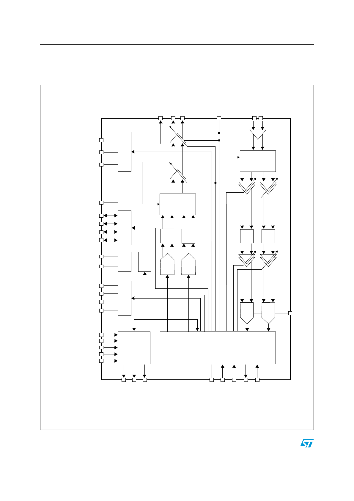
VDDA_ADC
SpiRxD
SpiTxD
SpiSSn
SpiClk
VDD1V2Cap
µCIRQ
µCReset
POnReset
Te st
TestRxN
TestRxP
TestCom
AnalogueVcc
AnalogueGND
DigitalVcc
Xtal32kN
Xtal32kP
D0
D1
D2
D3
RRef
Xtal32MN
Xtal32MP
VDDA_DCO
VBalun
DigitalGND
TxP
TxN
Tx/Rx
RxP
TxP
µCVcc
MCU
Chirp
Pulse
Sequencer
Digital
Processing
Battery
Digital I/O
Synthesizer
32 kHz
Osc
RTC
DAC
DAC
ADC
ADC
LPF
LPF
LPF
LPF
IQ DEMOD
IQ DEMOD
I
Q
I
Q
VGA
VGA VGA
VGA
LNA
PA
2 TN100 block diagram
Figure 1. Simplified TN100 block diagram
14/235

TN100 Key features
3 Key features
The TN100 transceiver incorporates robust wireless communication capabilities including:
● Built-in precise ranging capabilities
● Channelization using FDMA for improved coexistence
● Different symbol durations and symbol rates
● Standard set of default register values set into chip
● Digital Dispersive Delay Line (DDDL) incorporated in the chip
● Programmable pull resistors
3.1 Built-in ranging capability
The TN100 transceiver provides a built-in ranging capability. The chip can be enabled to
provide Round Trip of Flight (RToF) information using a special Data / Ack packet
transmission. Because the processing time for generating a hardware acknowledgment is
known and the time of transmission a data packet is known, these two values can be used to
calculate a ranging distance between the two TN100 stations.
3.2 Channelization using FDMA for improved coexistence
Channelization is the subdividing of the available frequency band (in this case, the 83 MHz
ISM band) into many narrow frequency bands, which for the TN100 transceiver is 22 MHz
channels. This increases coexistence with devices sharing the same ISM band. The TN100
transceiver channelizes the 2.4 GHz ISM band into multiple 22 MHz frequency channels
using Frequency Division Multiple Access (FDMA). With register settings, the chip can be
set to 80 MHz or 22 MHz signal bandwidth. The chip is set by default to use FDMA on
startup and can be programmed to use one of multiple 22 MHz channels in the ISM band.
3.3 Incorporated digital dispersive delay-line (DDDL)
The TN100 transceiver incorporates a Digital Dispersive Delay Line (DDDL), which in
previous chips was an external component. Reference values for I and Q can be stored in
Baseband RAM. These values are used to detect incoming signals generated by another
transceiver chip. The detectable signals can be one of the following:
● An Upchirp (linear frequency modulation, where frequency increases in time)
● A Downchirp (linear frequency modulation, where frequency decreases in time)
● An OffChirp, which is the absence of a chirp
Note: For more details, see Section 20: Chirp modulation on page 89.
3.4 Selectable symbol durations and symbol rates
The TN100 transceiver provides selectable symbol durations and symbol rates.
● Symbol durations include: 0.5 µs, 1 µs, 2 µs, and 4 µs
● Symbol rates include: 2 Mbps, 1 Mbps, 0.5 Mbps and 0.25 Mbps
Note: See Section 26.2.61: 0x48 – Symbol duration, symbol rate, and modulation system on
page 169.
15/235

Architecture TN100
4 Architecture
The TN100 is a extremely low power, highly integrated mixed signal chip incorporating both
an analog and a digital part in one silicon die. This section provides a brief overview of the
digital and analog parts of the chip.
4.1 Analog part - TX and RX
For transmission, the analog part of the chip converts data obtained from the digital part into
chirp pulses and sends packets over the air using an RF link. For reception, it detects
received chirp pulses into a form that can be used by the digital part.
4.2 Digital part - programming interface
The digital part of the chip provides an SPI interface for reading and writing to chip registers.
Application data is written to chip buffers in the digital part, which is then provided to the
analog part of the chip for transmission over the air. Data received from the analog part is
provided to an application via buffers in the digital part. To achieve maximum power savings,
the digital part of the TN100 transceiver is divided into two sections called an ON section
(that is, always powered) and a PWD section (that is, powered during operating mode).
4.2.1 Digital part – ON Section
The ON section, which is always powered, contains the minimum number of required
controls that are used to maintain the chip settings. It also is connected to the digital I/O pins
as these pins are used for power management.
4.2.2 Digital part – PWD section
The PWD section, which is powered up only during operating mode, contains the remaining
controls that are used when the chip is required for data transmission and reception.
16/235

TN100 Architecture
Analog
Application
data sent
and
received
over SPI
interface
ON PWD
Always powered
Only powered when
chip is in
operating mode
Packets
sent and
received
over an RF
Link
PINS
PINS
PINS
4.3 Signal flow
Figure 2 illustrates the signal flow within the chip.
Figure 2. Signal flow in the TN100 transceiver
4.4 Commonly used set of register default values
The chip has been set with a number of default values that would be required for most
standard applications to reduce the time required for chip initialization.
Note: A full listing of register default values is provided in Appendix B: Default register settings on
page 224.
4.5 Programmable pull-resistors
The TN100 transceiver uses programmable pull-resistors to lower the cost of the bill of
materials. The following pads can now be set as either pull-up or pull-down:
● SpiClk (pin 15)
● SpiSsn (pin 16)
● SpiTxd (pin 17)
● SpiRxd (pin 18)
● POnReset (pin 30)
● TxRx (pin 9)
● µCIRQ (pin 27)
● µCReset (pin 28)
● Digital IO pads (pins 19 to 22)
17/235
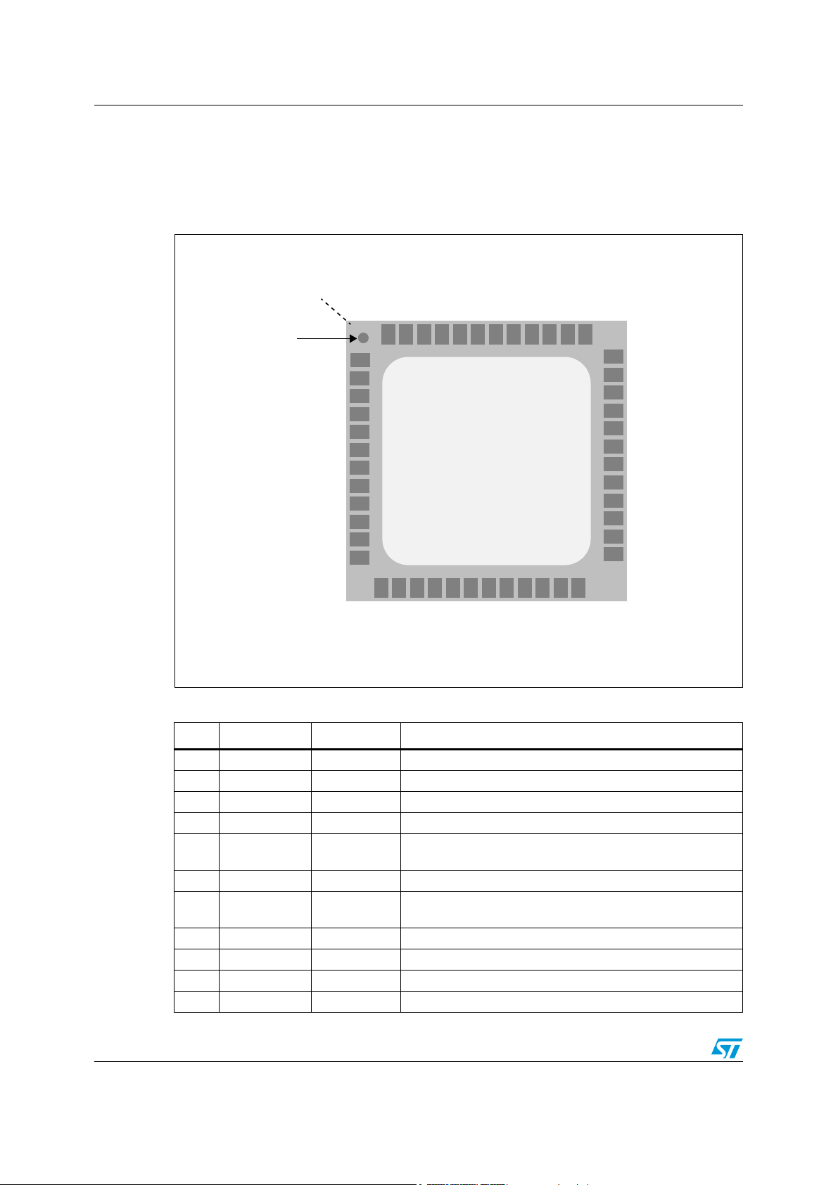
Pin description TN100
1
2
3
4
5
6
7
8
9
10
11
12
15 18 19 21 22 23 242016 171413
31
30
29
28
27
26
25
35
34
33
32
36
48 43 42 40 39 38 3741454647 44
VDDA
RRfef
VSSA
VDDA_DCO
Xtal32kP
Xtal32kN
Xtal32MP
Xtal32MN
Tx/Rx
VSSD
VSSD
VDDD
VDDD
VSSD
SpiClk
/SpiSsn
SpiTxD
SpiRxD
D0D1D2
D3
VSSD
VDDD
VSSD
µCReset
µCIRQ
VDD1V2_Cap
µCVcc
/POnReset
VSSD
VDDA_ADC
nc
VSSA
VDDA
VDDA
nc
nc
VSSA
VSSA
RxN
RxP
VSSA
TxN
TxP
VSSA
VBalun
VDDA
Pin 1 Identification
GND
Exposed die
attach pad
5 Pin description
This section provides a brief overview of the location and function of each pin.
Figure 3. Pinout
18/235
Table 1. Pin descriptions
Pin Signal Direction Description
1 VDDA Supply Power supply for analog parts
2 RRef Analog IO Pin for external reference resistor
3 VSSA Supply Power supply for analog parts
4 VDDA_DCO Supply Power supply for DCO
5 Xtal32kP Analog IO
6 Xtal32kN Analog IO Crystal 32768 Hz
7 Xtal32MP Analog IO
8 Xtal32MN Analog IO 32.0 MHz crystal oscillator
9 Tx/Rx Digital output Output signal to distinguish between transmit and receive
10 VSSD Supply Power supply for digital parts
11 VSSD Supply Power supply for digital parts
Crystal 32768 Hz, input from external 32768 Hz frequency
reference
32.0 MHz crystal oscillator, input from external 32 MHz
frequency reference

TN100 Pin description
Table 1. Pin descriptions (continued)
Pin Signal Direction Description
12 VDDD Supply Power supply for digital parts
13 VDDD Supply Power supply for digital parts
14 VSSD Supply Power supply for digital parts
15 SpiClk Digital input SPI clock
16 SpiSSn Digital input SPI slave selected
17 SpiTxD Digital output SPI transmit data (MISO)
18 SpiRxD Digital Input SPI receive data (MOSI)
19 D0 Digital IO Digital input or output line 0
20 D1 Digital IO Digital input or output line 1
21 D2 Digital IO Digital input or output line 2
22 D3 Digital IO Digital input or output line 3
23 VSSD Supply Power supply for digital parts
24 VDDD Supply Power supply for digital parts
25 Test Digital IO Pin for digital tests
26 µCReset Digital output Reset for external microprocessor
27 µCIRQ Digital output Interrupt request to external microprocessor
28 VDD1V2_CAP Supply 1.2 V digital power supply decoupling.
29 µCVCC Supply Switchable power supply for external microcontroller
30 POnReset Digital input Power on reset line
31 VSSD Supply Power supply for digital parts
32 VDDA_ADC Supply Power supply for analog parts (Rx ADC)
33 TestCom LF signal Test pin for analogue signals
34 VSSA Supply Power supply for analog parts
35 VDDA Supply Power supply for analog parts
36 VDDA Supply Power supply for analog parts
37 TestRxP LF Signal Test pin for RX signals
38 TestRxN LF Signal Test pin for RX signals inverted
39 VSSA Supply Power supply for analog parts
40 VSSA Supply Power supply for analog parts
41 RxN RF input Differential receiver input (inverted)
42 RxP RF input Differential receiver input
43 VSSA Supply Power supply for analog parts
44 TxN RF output Differential transmitter output (inverted)
45 TxP RF output Differential transmitter output
46 VSSA Supply Power supply for analog parts
Power supply for external balun (DC for TxP/TxN; needs to
47 VBalun Supply
48 VDDA Supply Power supply for analog parts
be blocked with an external capacitor in the 27pF to 47pF
range close to the balun)
19/235

Pin description TN100
5.1 Input and/or output pins
Ta bl e 2 describes the digital pins and analog pins of the TN100 transceiver.
Table 2. Digital input pins
Pin Pin no. Direction Description
Analog pin. 32.768 kHz crystal oscillator pin 1 or input
Xtal32kP 5 Input
Xtal32kN 6 Output Analog pin. 32.768 kHz crystal oscillator pin 2.
Xtal32MP 7 Input
Xtal32MN 8 Output Analog pin. 32 MHz kHz crystal oscillator pin 2.
/POnReset 30 Input Power on reset signal.
SpiClk 15 Input
/SpiSSn 16 Input
for an external 32.768 kHz clock generator. Used to
connect crystal or active frequency reference.
Analog pin. 32 MHz crystal oscillator pin 1 or input for
an external 32 MHz clock generator. Used to connect
crystal or active frequency reference.
The SPI Clock is generated by the microcontroller
(master) and synchronizes data movement in and out of
the device through the pins SpiRxD and SpiTxD.
SPI Slave Select (low active) is externally asserted
before the microcontroller (master) can exchange data
with the TN100 transceiver. Must be low before data
transactions and must stay low for the duration of the
transaction.
SpiRxD 18 Input SPI Receive Data (MOSI).
SpiTxD 17 Output SPI Transmit Data (MISO).
Distinguishes between the TX and RX phase. Can also
Tx/Rx 9 Output
µCReset 26 Output Reset for external microprocessor.
µCIRQ 27 Output Interrupt request to external microprocessor.
D0 19 Input/Output
D1 20 Input/Output
D2 21 Input/Output
D3 22 Input/Output
µCVcc 29 Output Analog pin. Power supply for external microprocessor.
be used to provide an external power amplifier control.
Active Low during TX, otherwise High.
Digital Input or Output (programmable, see
configuration bits below), line 0.
Digital Input or Output (programmable, see
configuration bits below), line 1.
Digital Input or Output (programmable, see
configuration bits below), line 2
Digital Input or Output (programmable, see
configuration bits below), line 3. Note that a 32.768 kHz
clock operates on this pin after reset/power up.
20/235

TN100 Pin description
5.2 Configuring the digital I/O pins – D0 to D3 (pins 19 to 22)
Each digital I/O pin can be configured as either an input or an output pin. Signal levels or an
alarm occurrence can be reported at a digital I/O pin that has been set as input. Ta bl e 3 lists
the fields are used for configuring digital I/O pins.
Table 3. Digital I/O pin configuration
Field Offset R/W Description
DioDirection 0x04 WO
DioOutValueAlarmEnable 0x04 WO
DioAlarmStart 0x04 WO
DioAlarmPolarity 0x04 WO
DioUsePullup 0x04 WO
DioUsePulldown 0x04 WO
Controls the direction of Digital I/O port. Set it
as either an input or an output pin.
When a Digital I/O port is configured as input,
this bit selects to be reported either the signal
level at the port or the occurrence of an
alarm.
Starts the alarm, and is set after the digital I/O
port is configured to report the occurrence of
an alarm.
When the digital I/O port is configured as an
input that should report the occurrence of an
alarm, then this bit is used to select the edge
which should trigger the alarm.
When the digital I/O port is configured as an
output, then this bit selects whether the value
programmed in DioOutValueAlarmEnable or
the feature clock should be driven out of the
digital I/O port.
When set to true, a pull-up resistor is
connected to the corresponding digital I/O
pad.
When set to true, a pull-down resistor is
connected to the corresponding digital I/O
pad only, but when DioUsePullup is false.
Each digital I/O pin has one write strobe, as listed in Tab l e 4 .
Table 4. Digital I/O pin write strobe
Field Offset R/W Description
DioPortWe 0x04 WO
Writes the settings of the 6 configuration bits
to the digital I/O controller.
Each digital I/O pin has one status bit, as listed in Tab l e 5 .
Table 5. Digital I/O pin status
Field Offset R/W Description
Each bit reports the signal level or the
occurrence of an alarm at one of the four
DioInValueAlarmStatus 0x04 RO
21/235
digital I/O ports, where bit 0 belongs to D0, bit
1 belongs to D1, bit 2 belongs to D2, and bit 3
belongs to D3.
Pin description TN100
V level
Start of
internal reset
Time
t
min
t
delay
Stop
Threshold
levels
High ≥ V
DDD
* 0.7
Low
# V
DDD
* 0.2
5 µs
≥ 400 µs
IC Ready
5.3 Configuring the IRQ Pin – µCIRQ (pin 27)
The IRQ pin (µCIRQ) can be configured with either a high or low active polarity and can be
driven as either push-pull or open-drain. The source of the interrupt can also be set.
The following fields are used to configure the IRQ pins as either low or high active, as well
as either push-pull or open-drain:
Table 6. IRQ pin configuration
Field Offset R/W Default
IrqPolarity
(high/low active)
IrqDriver
(push-pull/open-drain)
0x00 RW
0x00 RW
Defines the polarity of the IRQ signal as either high or
low active. The default is low active.
Switches between push-pull or open-drain for IRQ
output driver. The default is open-drain.
The following fields are used to drive the interrupt of the IRQ pin by either a transmitter
interrupt, a receiver interrupt, a baseband timer interrupt, or a local oscillator interrupt:
Table 7. Interrupts driving the IRQ pin
Field Offset R/W Description
TxIrqEnable
RxIrqEnable
BbTimerIrqEnable
LoIrqEnable
0x0F RW
0x0F RW
0x0F RW
0x0F RW
The transmitter interrupt can be enabled to drive the
interrupt line. Default is disabled.
The receiver interrupt can be enabled to drive the
interrupt line. Default is disabled.
The baseband timer can be enabled to drive the
interrupt line. Default is disabled.
The Local Oscillator interrupt can be enabled to drive
the interrupt line. Default is disabled.
5.4 Power-on reset – /POnReset (pin 30)
/POnReset signal is active low. Figure 4 shows a timing diagram for /POnReset.
Figure 4. /POnReset timing diagram
22/235

TN100 Memory map
Address
Memory
Typ e
Page
Select
Register
Select
Bits 6-0
11-10 9-8 7
Hex FFF
11
11
1 Correlator RAM Page 3
0
Register Block
10
1 Correlator RAM Page 2
0 Register Block
01
1 Correlator RAM Page 1
0 Register Block
00
1 Correlator RAM Page 0
Hex C00 0 Register Block
Hex BFF
10
11
1 Chirp Sequencer Page 3
0 Register Block
10
1 Chirp Sequencer Page 2
0 Register Block
01
1 Chirp Sequencer Page 1
0 Register Block
00
1 Chirp Sequencer Page 0
Hex 800 0
Register Block
Hex 7FF
01
Hex 400
Hex 3FF
00
11
1 Baseband Page 3
0 Register Block
10
1 Baseband Page 2
0 Register Block
01
1 Baseband Page 1
0 Register Block
00
1 Baseband Page 0
Hex 000 0
Register Block
Correlator RAM
Chirp Sequencer
Baseband RAM
Unused
6 Memory map
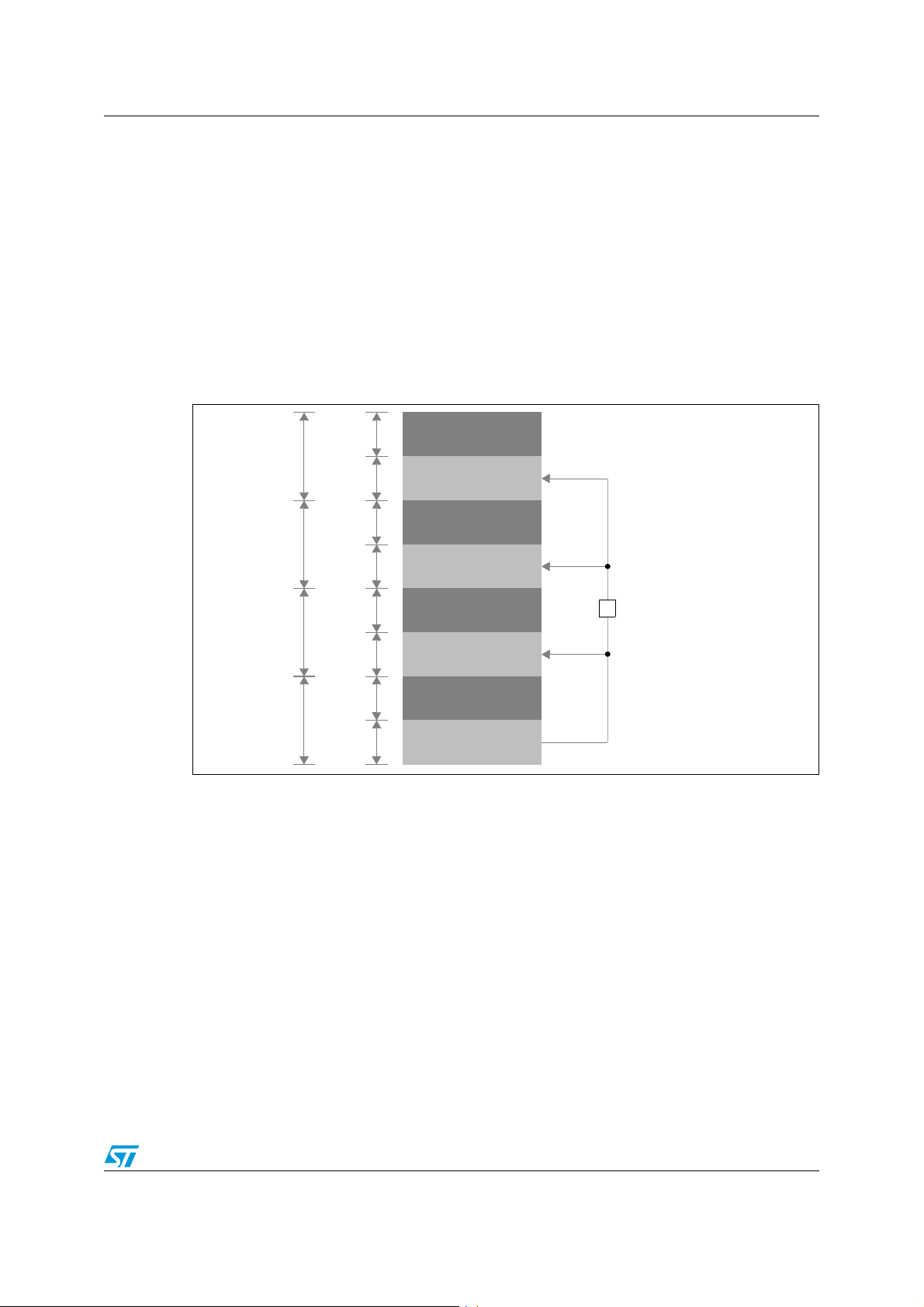
This section describes the memory map of the TN100 transceiver. Procedures are provided
for accessing the chip’s programmable Register Block, as well the Baseband RAM, Chirp
Sequencer RAM, and Correlator RAM. Figure 5 shows the memory map of the TN100
transceiver.
Figure 5. Memory map
23/235

Memory map TN100
Ta bl e 8 lists the sections provided in the memory map.
Table 8. Memory map section
Address Memory type Description
0x000 to
0x3FF
0x800 to
0xBFF
0xC00 to
0xFFF
0x000 to
0x07F
Baseband RAM
Chirp Sequencer
RAM
Correlator RAM
Register Block
512 bytes of Baseband RAM stores both data payload and MAC
header values, depending on buffer configuration settings.
Delivers two sequences of 6-bit values that synthesize the I and Q
signals of a symbol.
Stores the reference and threshold values for detection. It is are
initialized with the FDMA, 4 µs default detector matrix. When other
symbols are needed this register must be programmed with the
appropriate values. The threshold must be programmed with the
appropriate value in any case (even for the default matrix).
128-byte programmable chip register block provides chip
configuration settings and is mapped to the entire memory of the
TN100 transceiver.
Note: For a description of the Chirp sequencer, see Section 10: Chirp sequencer (CSQ) on
page 53. The Correlator RAM is described in Section 6.3: Correlator RAM access on
page 26. The Register Block is described in Section 6.2: 128-byte programmable register
block on page 25.
6.1 Selecting a memory address
There are two ways to access the TN100 transceiver memory map: direct and indirect
access. The Register block is accessed using a direct access model. The Baseband, Chirp
Sequencer and Correlator RAM blocks are accessed using an indirect access model.
To access one of these RAM blocks using an indirect access model through register 0x0E –
Baseband memory access:
1. Select the memory type (Baseband, Chirp Sequencer or Correlator) using bits
DeviceSelect.
2. Select the page pointer using bits RamIndex.
3. A Read or Write operation can now be performed.
For example to write a value to the Chirp Sequencer RAM at location 0x185, write in register
0x0E – Baseband memory access:
1. Write DeviceSelect = 0x2 to select the Chirp Sequencer
2. Write RamIndex = 0x1 to select the RAM column 1.
3. Write to address 0x85.
For example to read a value from the Correlator RAM location at 0x280, write in register
0x0E – Baseband memory access:
1. Write DeviceSelect = 0x03 to select the Correlator RAM.
2. Write RamIndex = 0x02 to select the Threshold.
3. Read from address 0x80.
Note: For a Read or Write operation at an address higher than 0x7F, the absolute address is
always relative to the value stored in register 0x0E.
24/235
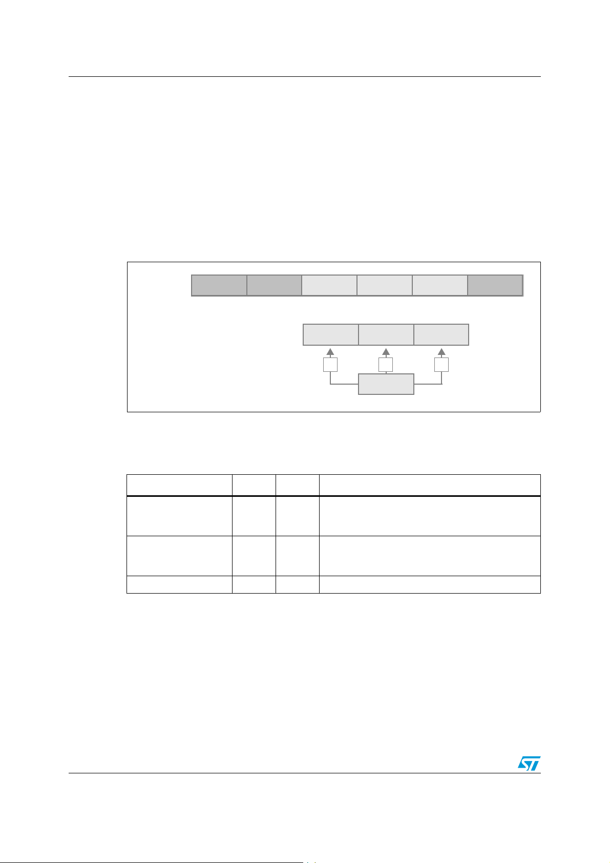
TN100 Memory map
Baseband RAM 3
Register
128 bytes
0x300
0x37F
0x380
0x3FF
128 bytes
Baseband RAM 2
Register
128 bytes
0x200
0x27F
0x280
0x2FF
128 bytes
Baseband RAM 1
Register
128 bytes
0x100
0x17F
0x180
0x1FF
128 bytes
Baseband RAM 0
Register
128 bytes
0x000
0x07F
0x080
0x0FF
128 bytes
≅
Page 0
Page 1
Page 2
Page 3
First mapping of register
block
Second mapping of register
block
Third mapping of register
block
Register block
6.2 128-byte programmable register block
The TN100 transceiver provides a 128-byte programmable register block for chip
configuration settings. The address space for the register is from 0x00 to 0xFF. However, it
is mapped to three additional mapped registers within the 1024-byte memory space of the
baseband RAM, where:
● Page 1 begins at offset 0x100
● Page 2 begins at offset 0x200
● Page 3 begins at offset 0x300.
These three mapped registers are logically equivalent to the register memory locations 0x00
to 0x7F. Figure 6 illustrates this mapping.
Figure 6. Register mapping in the 1024-byte TN100 memory space
Note: All user accessible registers in this register block is fully described in Section 26.2:
Description of chip registers on page 125.
6.2.1 Accessing a register address location
To access a memory location in the register only one SPI transfer is required, where:
● SPI Address[7] = 0
● SPI Address[6:0] = <offset address in register>
Note: A wraparound SPI burst transfer leads to unpredictable behavior. A wraparound SPI burst is
Either an SPI single byte operation or an SPI burst transfer can be used to access chip
memory. The lower 7 bits of a given memory location are identical with the start address in
the selected segment. SPI burst transfers are limited to 128 bytes (which is the segment
size).
when the number of bytes to be accessed is greater than the number of bytes from the start
address to the end of the segment.
25/235

Memory map TN100
6.2.2 Setting a shadow variable for the RAM access register
When bit 7 of the 10 bit memory address is 1, the RamIndex field must be set with the two
highest bits of this address (shifting right by 8 positions). The lower 8 bits are directly used in
the next SPI access, which writes this data.
To reduce the overhead caused by writing the RamIndex field for each memory access, it is
recommended that an RamIndex shadow variable be maintained in software. This variable
can be used to back up the last value of the RamIndex field. If address locations in the
same segment are accessed sequentially, write operations to the RamIndex field can be
eliminated by comparing the RamIndex value with the shadow variable.
6.3 Correlator RAM access
The Correlator RAM contains the reference sequences of the detector and the detection
thresholds. Use Correlator Memory I for programming the In-Phase values of the detector
and use Correlator Memory Q for Quadrature-Phase values. Use Correlator Memory
Thresholds to set the thresholds for In-Phase and Quadrature-Phase detection.
A Correlator RAM page is selected by setting DeviceSelect and RamIndex as shown in
Ta bl e 9 .
Table 9. Selecting a correlator RAM page
DeviceSelect setting RAMIndex setting Selected correlator memory page
RamIndex = 0x0 (default value) I (RamD3IPatI)
DeviceSelect =
0x3
RamIndex = 0x1 Q (RamD3IPatQ)
RamIndex = 0x2 Thresholds (RamD3IThresholds)
RamIndex = 0x3 Unused
6.4 Chirp sequencer RAM access
The Chirp Sequencer (CSQ) RAM space contains the values for I and Q, which are used to
calculate Upchirps and Downchirps. The CSQ is set with a default matrix that has a symbol
duration of 4 µs (4000 ns) and a 22 MHz bandwidth.
A Chirp Sequencer RAM page is selected by setting DeviceSelect and RamIndex as
shown in Ta bl e 1 0.
Table 10. Selecting a correlator RAM page
DeviceSelect setting RAMIndex setting Selected correlator memory page
RamIndex = 0x0 (default value) Column 0
DeviceSelect =
0x2
RamIndex = 0x1 Column 1
RamIndex = 0x2 Column 2
RamIndex = 0x3 Unused
Note: For more details about the Chirp Sequencer, see Section 10: Chirp sequencer (CSQ) on
page 53.
26/235

TN100 Clocking structure
Digital IO Control
ON PWD
DDDL Memory
SPI Controller
Real-Time Clock
CSQ Memory
Others
Baseband Control
Radio Control
Power Management
(4 kHz)
D[3:0]
Tx/Rx
SPI
µCirq
µCReset
µCVcc
Protection
32.786 kHz clock:
SPI clock:
32 MHz Baseband clock:
CSQ (Chirp Sequencer) clock:
7 Clocking structure
This section describes the four clocks provided by the TN100 transceiver: 32.768 kHz clock,
SPI clock, 32 MHz baseband clock, and the Chirp Sequencer (CSQ) clock.
7.1 Overview
The TN100 transceiver provides the following four clocks:
32.786 kHz clock – Used to run the real-time clock and power management.
SPI clock – Used for the SPI Controller and for the Digital IO Control used for
running the four digital IO pins. The frequency of the SPI clock is dependent on the
frequency required by the microcontroller. The maximum frequency is 27 MHz.
32 MHz baseband clock – Used for baseband control, radio control, and other
baseband uses. The frequency of the baseband clock for the TN100 transceiver is
32 MHz and can be enabled or disabled by software.
CSQ (Chirp Sequencer) Clock – Used by the Chirp Sequencer (CSQ) Memory.
The frequency of the CSQ clock is determined by dividing the Local Oscillator (LO)
frequency by 10. The CSQ clock can be enabled or disabled by software.
Figure 7. Clock structure
7.2 32.786 kHz real-time clock (RTC)
This real-time clock (RTC) runs at 32.768 kHz. It can be set or read through software using
a 48-bit real-time clock value. As this clock is part of the ON section of the chip’s digital part,
it is always powered (unless the chip is completely powered off) and can, therefore, be used
for creating a wake-up time event.
27/235

Clocking structure TN100
ON PWD
Real-Time Clock
Power Management
(4 kHz)
D[3:0]
Tx/Rx
SPI
µCIRQ
µCReset
µCVcc
Protection
32.786 kHz Clock:
The real-time clock is also used to generate a 4 kHz clock (the Power Management clock)
for use by the Power Management module in the ON section. Like the real-time clock, this
slow clock is always available during power down mode to protect the connections between
the SPI and the SPI Controller.
Figure 8 shows the real-time clock and Power Management modules that use the 32.768
kHz RTC.
Figure 8. 32.786 kHz real-time clock
7.2.1 Updating and reading the RTC through software
The 48-bit real-time clock is set and read through software. Since the real-time clock is
updated every 1/(32.768 kHz), it is not directly accessible by the user. A RAM buffer
RamRtcReg is used to hold the value of the internal real-time clock after it has been read.
This buffer is also used to hold a value that will be written to the real-time clock.
Fields for updating RTC by software
Ta bl e 1 1 lists the fields used for updating the real-time clock with software.
Table 11. RTC and TimeB packets
Field Offset R/W Description
RtcCmdWr 0x62 WO Writes the 48-bit RTC value.
RtcCmdRd 0x62 WO Reads the 48-bit RTC value
48-bit RTC value read from the RTC by software or
written to the RTC by software
RamRtcReg 0xF0 RW
Updating the value of the RTC
To update the value of the real-time clock, do the following
1. Write a 48-bit value for the real-time clock to the buffer RamRtcReg.
2. Write this buffer to the real-time clock using the write command RtcCmdWr.
28/235

TN100 Clocking structure
Reading the value of the RTC
To read the value of the real-time clock, do the following:
1. Read the real-time clock using the read command RtcCmdRd to place the 48-bit value
of the real-time clock in the buffer RamRtcReg.
2. Read out the buffer RamRtcReg.
7.2.2 Manually or automatically updating the RTC using TimeB packets
The real-time clock can also be updated from TimeB packets that have been sent from a
base station or other stations in a network. This updating can be performed automatically or
manually.
If the updating is performed automatically, then when a TimeB packet is received, the RTC
value in the packet is automatically written to the real-time clock.
If the updating is performed manually, then when a TimeB packet is received, the RTC value
in the packet must be manually updated as described in Section 7.2.1: Updating and
reading the RTC through software on page 28.
Fields for updating RTC by TimeB packets
Ta bl e 1 2 lists the fields used for updating the real-time clock by TimeB packets.
Table 12. RTC and TimeB packets
Field Offset R/W Description
RtcTimeBAutoMode 0x62 WO
RtcTimeBRxAdj 0x61 WO Adjusts the RTC value for receiver delay.
RtcTimeBTxAdj 0x60 WO Adjusts the RTC value for transmitter delay
RamRtcTx 0xE0 RW
RamRtcRx 0xE8 RW
When set to 1, the RTC value is transferred in TimeB
packets
The 48-bit RTC value that is to be transmitted
(loaded/written) in a TimeB packet
The 48-bit RTC value that has been received in a
TimeB packet
Manually updating the RTC
To manually update the real-time clock through the RTC value in a TimeB packet, enable
Manual mode for TimeB packets by setting:
RtcTimeBAutoMode = NA_RtcTimeBAutoModeOff_BC_C (0x0)
This causes the 48-bit RTC value in the received TimeB packets to be stored in the real-time
clock buffer RamRtcReg, where it can then be written to the real-time clock using the write
command RtcCmdWr.
Automatically updating the RTC
To automatically update the real-time clock through from the RTC value in a TimeB packet,
enable Auto mode for TimeB packets by setting:
RtcTimeBAutoMode = NA_RtcTimeBAutoModeOn_BC_C (0x1)
This causes the RTC values in received TimeB packets to be automatically stored in the
real-time clock.
29/235
Clocking structure TN100
47 31 8
023
70
3 12
RtcWakeUpTime
(RTC)
Wake Uptim e
WakeUpti meB yte We
WakeUptimeByte
0
7.2.3 Using the RTC as wake-up event
The real-time clock can be used to create a wake-up time event at a predefined time. The
field EnableWakeUpRtc enables the real-time clock to be used as a wake-up event.
The RTC wake-up time is set in RtcWakeUpTime but can only be accessed through the use
of WakeUpTimeByte and WakeUpTimeWe.
The wake-up time is a 24-bit value split into 3 bytes. The field WakeUpTimeByte is used to
set each of the three segments of the wake-up time (the segment to write is selected using
the a byte-selector field WakeUpTimeWe). This wake-up time value is then compared to bits
31 to 8 of the real-time clock. When these values match, a wake-up event is then triggered.
This process is shown in Figure 9.
Figure 9. Using real-time clock as wake-up event
Fields for setting RTC as wake-up event
Ta bl e 1 3 lists the fields using the real-time clock as a wake-up time event.
Table 13. Wake-up time fields
Field Offset R/W Description
Stores a one byte value for the wake-up time, which
WakeUpTimeByte 0x01 WO
WakeUpTimeWe 0x02 WO
EnableWakeUpRtc 0x06 RW Enable real-time clock as Wake-Up Source
is programed to the wake-up time RtcWakeUpTime
using WakeUpTimeWe.
Loads the value of RtcWakeUpTimeByte to the
appropriate byte of the wake-up time in the wake-up
time circuitry.
7.3 SPI clock
The SPI Clock is an externally delivered clock provided to the chip through an SPI signal
from a master device, such as a microcontroller. The frequency of the SPI clock is
dependent on the frequency of the master device. The maximum frequency of the SPI clock,
however, is 27 MHz. It is provided as one of the four signals of the SPI interface: SpiClk.
Figure 10 shows the Digital IO Control and DDDL Memory modules as well as the SPI
Controller that use the SPI clock.
30/235

TN100 Clocking structure
Digital IO Control
ON PWD
DDDL Memory
SPI Controller
D[3:0]
Tx/Rx
SPI
µCIRQ
µCReset
µCVcc
SPI Clock:
ON PWD
Others
Baseband Control
Radio Control
32-MHz Baseband clock:
D[3:0]
Tx/Rx
SPI
µCIRQ
µCReset
µCVcc
Figure 10. SPI clock
This clock is used to run the SPI Controller. As the Digital I/O Control is run by the SPI
Controller, the SPI Clock is also used to run the four digital I/O pins: D0, D1, D2 and D3. It
also runs all registers that are written by the SPI Controller.
7.4 32-MHz baseband clock
The baseband clock distribution obtains its frequency from the internal quartz oscillator. In
the TN100 transceiver, the internal quartz oscillator provides a 32-MHz frequency. This
clock is used for baseband control, radio control, and other baseband uses.
Figure 11. 32-MHz baseband clock
Note: The baseband clock can be enabled and disabled by software.
As the baseband clock is within the PWD section, this clock and all its modules run by this
clock are powered off when the chip goes into PowerDownModeFull. Consequently, the
contents of all chip registers are also lost.
31/235

Clocking structure TN100
IC boundary
Crystal
Oscillator
Clock
gate
Internal power
supply bus
Step 3: EnableBbCrystal
Xtal32MP
Xtal32MN
32 MHz
Step 2: ResetBbClockGate
Step 1: EnableBbClock
RST
RST
D
Enable
Clock
Q
1
Baseband
clock
Table 14. Baseband clock related fields
Field Offset R/W Description
ResetBbClockGate 0x07 RW Resets the baseband clock distribution circuitry.
ResetBbRadioCtrl 0x07 RW
Resets the digital baseband and radio control
circuitries.
EnableBbCrystal 0x08 RW Powers on the internal baseband oscillator.
EnableBbClock 0x08 RW Enable the baseband clock distribution.
7.4.1 Stopping / enabling the 32-MHz baseband clock
To reduce power consumption without losing the contents of chip registers, the baseband
clock distribution can be stopped and the quartz oscillator circuitry can be powered down.
Figure 12 shows the 32-MHz baseband clock and baseband quartz oscillator circuitry.
Figure 12. Switching on/off the baseband clock
Keeping clock switcher in stable state
The clock switcher is kept in a stable state during warm-up and shut down of the quartz
oscillator by using ResetBbClockGate.
Stopping the 32-MHz baseband clock distribution
To stop the baseband clock distribution, do the following:
1. Set EnableBbClock = 0 to switch off the baseband clock distribution.
2. Set ResetBbClockGate = 1 to enable active reset of the baseband clock circuitry.
3. Set EnableBbCrystal = 0 to power off the internal baseband quartz oscillator.
Enabling the 32-MHz baseband clock distribution
To enable the baseband clock distribution, do the following:
1. Set EnableBbCrystal = 1 to power on the internal baseband quartz oscillator.
2. Set ResetBbClockGate = 0 to inactivate the reset of the baseband clock circuitry.
3. Set EnableBbClock = 1 to switch on the baseband clock distribution.
32/235

TN100 Clocking structure
ON PWD
CSQ Memory
CSQ (Chirp Sequencer) Clock:
D[3:0]
Tx/Rx
SPI
µCIRQ
µCReset
µCVcc
7.5 CSQ (Chirp Sequencer) clock
The Chirp Sequencer clock (CSQ) is required for programming the Chirp Sequencer RAM
memory. The frequency of the CSQ clock is determined by dividing the Local Oscillator (LO)
frequency by 10 (see Section 21.2: Calibrating the local oscillator frequency on page 92).
The CSQ clock can be enabled or disabled by software using EnableCsqClock.
Figure 13 shows the CSQ Memory module that uses the Chirp Sequencer clock.
Figure 13. Chirp sequencer clock
Table 15. Chirp sequencer clock related fields
Field Offset R/W Description
EnableCsqClock 0x42 RW Enables the Chirp Sequencer (CSQ) clock.
7.5.1 Stopping / enabling the Chirp Sequencer clock (CSQ)
Enabling the Chirp sequencer clock
1. LOenable=1
2. LODiv10enable=1
3. EnableCsqClock=1
Disabling the Chirp sequencer clock
1. EnableCsqClock=0
2. LODiv10enable=0
3. LOenable=1
7.5.2 Using the default matrix for transmission
To use the default matrix for transmission, set CsqUseRam = 0.
Note: ‘0’ is the default value of CsqUseRam.
33/235

Power management TN100
8 Power management
This section describes the five power management states of the TN100 transceiver, which
are PwrDownModeFull, PwrDownModePad, PowerUp, Standby, and Ready.
The TN100 transceiver is designed to efficiently use the power required to operate the chip.
Modules required during transmission and reception, such as the baseband memory, CSQ
memory, the SPI Controller, and other modules are located in a section of the chip that can
be powered down when not in use. To keep the chip operational, the minimum required
modules are located in a section of the chip that uses minimal power to maintain a
connection with the microcontroller.
8.1 Power management states
Ta bl e 1 6 shows the current consumption and activation time of the power management
states.
Table 16. Power management states
State
PwrDownModeFull under 2.5 µA
PwrDownModePad # 600 µA
PowerUp # 700 µA
StandBy # 2.5 mA Ready (without reconfiguration) 6 µs
Ready # 4 mA n./a.
1. Current consumption values are typical values only.
2. @ 4 Mbit/s SPI.
Current
consumption
(1)
PowerUp: between 1 and 32 ms (programmable) + boot
time of the external microcontroller
PowerUp: between 1 and 32 ms (programmable) + boot
time of the external microcontroller
StandBy: # 5 ms (depending on the speed of the
baseband quartz oscillator)
Activation time into state
(2)
8.2 Power management module – ON and PWD sections
The Power Management module is located within a section called the “ON section.” It is
provided with a clock frequency of 4 kHz by the 32.768 kHz RTC. Figure 14 shows the ON
and PWD sections of the TN100 transceiver, with the modules contained within each
section. The connections between the pins and the ON and PWD sections are shown as
dashed lines, while connections protected by the Power Management module protects are
shown by the light lines.
34/235

TN100 Power management
Digital IO Control
ON PWD
DDDL Memory
SPI Controller
Real-Time Clock
CSQ Memory
Others
Baseband Control
Radio Control
Power Management
(4 kHz)
D[3:0]
Tx/Rx
SPI
µCIRQ
µCReset
µCVcc
Protection
Figure 14. Power management module
The Power Management module is responsible for maintaining the pull-up and pull-down
states of the SPI interface during all power down modes. This includes the pins: SpiClk,
SpiSSn, SpiRxD, and SpiTxD. This module is also responsible for maintaining the pull-up
and pull-down states of several additional input/output pins, including:
● /POnReset, an input pin which provides a signal to the power up reset line.
● TxRx, an output pin which is used to control an external power amplifier.
● µCReset, an output pin which resets an external microcontroller.
● µCIRQ, an output pin which sends interrupt requests to an external microcontroller.
The Digital IO pins are always powered as they can be programmed to provide a wake-up
event to bring the PWD section back to powered up state.
35/235

Power management TN100
Receive Mode
Internal baseband
clock distribution off
Internal baseband
clock distribution on
Configuration of
Wake Up Timers or
of alarm Events
Configuration of
Wake Up Timers or
of alarm Events
TX-INIT
TX RF-INIT
Calibrate-TX
Transmit Mode
RX-INIT
RX RF-INIT
Calibrate-RX
Station-INIT
Ready Mode
Standby Mode
Baseband quartz
clock off
Baseband quartz
clock on
Powerup Mode
Wake-up timer
or alarm events
Wake-up timer
or alarm events
Powerdown
PAD Mode
Powerdown
FULL Mode
8.3 Power management state model
The power management states model of the TN100 transceiver is shown in Figure 15.
Figure 15. Power management state model
8.4 Power management fields
36/235
Ta bl e 1 7 lists the fields used for Power Management.
Table 17. Power management related fields
Field Offset Description
EnableWakeUpRtc 0x06 RTC wake-up event brings the chip into the power up state.
Alarm event (rising/falling edge) at a digital IO configured as a
EnableWakeUpDio 0x06
wake-up source (see register 0x4) brings the chip into the power up
state.
PowerUpTime 0x06
PowerDownMode 0x06
PowerDown 0x07
Configures duration of the power-up time (duration of active
µCReset).
Selects the power down mode to use when the chip enters the
powered down state
Brings the chip to the configured power-down state. This bit will be
automatically cleared when the chip is powered-up.

TN100 Power management
Digital IO Control
ON PWD
DDDL Memory
SPI Controller
Real-Time Clock
CSQ Memory
Others
Baseband Control
Radio Control
Power Management
(4 kHz)
Protection
Powered =
D[3:0]
Tx/Rx
SPI
µCIRQ
µCReset
µCVcc
8.5 PowerDownModeFull state
When the chip is in PowerDownModeFull, it consumes less power but after power up the
chip will need to be reconfigured. The pins and registers of the chip are powered off but
reconfiguration of the registers is required after wake-up. Also leakage current is the lowest
possible in this mode.
Figure 16. PowerDownModeFull showing powered sections
Current Consumption
The current consumption
(a)
during PowerDownModeFull is under 2.5 µA.
Chip State
The chip is in the following state during PowerDownModeFull:
Table 18. PowerDownModeFull state
Module State
External Microcontroller (µcVcc) Powered down
PWD section Powered down (all register settings lost)
ON section Powered
Real-time clock Running
Wake-up timer Running
Digital IO Control Running
Power Management module Running
Setting PowerDownModeFull
To s e t PowerDownModeFull, do the following:
1. Set PowerDownMode = NA_PowerDownModeFull_C (0x0)
2. Set PowerDown = 1
a. Current consumption values are typical values only and are values without an external microcontroller and
where digital IO pads are tri-state or inputs and no external pull-up resistors soldered on pads.
37/235

Power management TN100
Digital IO Control
ON PWD
DDDL Memory
SPI Controller
Real-Time Clock
CSQ Memory
Others
Baseband Control
Radio Control
Power Management
(4 kHz)
Protection
Powered =
D[3:0]
Tx/Rx
SPI
µCIRQ
µCReset
µCVcc
Bringing to PowerUp State
Either an internal wake-up timer or an external event on a Digital IO pin brings the chip out
of PowerDownModeFull into PowerUp state. This activation time is programmable using the
field PowerUpTime in a range between 1 and 32 ms + boot time of the external
microcontroller. After the chip is in PowerUp mode, the external microcontroller can then
initialize and (optionally) calibrate the chip.
8.6 PowerDownModePad state
When the chip is in PowerDownModePad, it consumes more power than
PowerDownModeFull but after it has been powered up, it does not need to be reconfigured.
In this state, all output pads are disabled and all bi-directional pads are switched to input, but
all transceiver registers are still powered. Reconfiguration of the chip registers is not
required, but leakage current is higher.
Figure 17. PowerDownModePad showing powered sections
Current Consumption
The current consumption during PowerDownModePad state is approximately 600 µA.
Chip State
The chip is in the following state during PowerDownModePad:
Table 19. PowerDownModePad state
Module State
External Microcontroller (µcVcc) Powered down
PWD section Powered (all register settings maintained)
ON section Powered
Real-time clock Running
Wake-up timer Running
Digital IO Control Running
38/235
Power Management module Running

TN100 Power management
Digital IO Control
ON PWD
DDDL Memory
SPI Controller
Real-Time Clock
CSQ Memory
Others
Baseband Control
Radio Control
Power Management
(4 kHz)
Protection
Powered =
D[3:0]
Tx/Rx
SPI
µCIRQ
µCReset
µCVcc
Setting PowerDownModePad
To set PowerDownModePad, do the following:
1. Set PowerDownModePAD = NA_PowerDownModePad_C (0x1)
2. Set PowerDown = 1
Bringing to PowerUp State
Either an internal wake-up timer or an external event on a Digital IO pin brings the chip out
of PowerDownModePad. The chip then goes into PowerUp state. The activation time is
programmable using the field PowerUpTime in a range between 1 and 32 ms + boot time of
the external microcontroller. After the chip is set in Ready state, the external microcontroller
can then initialize and calibrate the chip.
8.7 PowerUp state
The chip enters PowerUp state from either PowerDownModeFull or PowerDownModePad
through on of the following: internal wake-up timer, external event on a Digital IO pin, or an
external reset
Figure 18. PowerUp state
Current Consumption
The current consumption during Powerup state is approximately 700 µA.
Chip State
When the chip is brought to PowerUp state, the following occurs:
Table 20. PowerUp state
Module State
External Microcontroller (µcVcc) Powered
From PowerDownModeFull to PowerUp PWD section powered and all pins are enabled
From PowerDownModePad to PowerUp
All output pins are enabled and digital IO pins are
switched to bi-directional
39/235

Power management TN100
Digital IO Control
ON PWD
DDDL Memory
SPI Controller
Real-Time Clock
CSQ Memory
Others
Baseband Control
Radio Control
Power Management
(4 kHz)
Protection
Powered =
D[3:0]
Tx/Rx
SPI
µCIRQ
µCReset
µCVcc
Table 20. PowerUp state (continued)
Module State
Real-time clock, Wake-up timer, and Power
Management module
Internal baseband quartz oscillator
Internal baseband modules
Running
Powered on and then baseband clock distribution is
switched off
Initiailzed with default settings and can now be
programmed via the SPI interface
Bringing to Standby state
When the chip is brought from PowerUp state into Standby state, all blocks are powered up
except the baseband distribution, which remains switched off. The activation time to bring
the chip into Standby state from PowerUp state is approximately 5 ms, depending on the
speed of the baseband quartz oscillator.
Wake-Up Sources for PowerUp state
The chip is brought to PowerUp state by a wake-up source. This is either a RTC wake-up
event or an alarm event (a rising or falling edge) at one of the digital IOs configured as a
wake-up source. Ta bl e 2 1 lists the fields used to set a wake-up event.
Table 21. Fields for setting a wake-up event
Field Offset Description
EnableWakeUpRtc 0x06
EnableWakeUpDio 0x06 Enable a digital IO pin as a wake-up source. Default is disabled.
Enable the Real-time clock as a wake-up source. Default is
disabled.
8.8 Standby state
When the chip is In Standby state, only the baseband clock distribution is switched off. All
other blocks of the chip are fully powered.
Figure 19. Standby state
40/235

TN100 Power management
Digital IO Control
ON PWD
DDDL Memory
SPI Controller
Real-Time Clock
CSQ Memory
Others
Baseband Control
Radio Control
Power Management
(4 kHz)
D[3:0]
Pamp
SPI
µCirq
µCReset
µCVcc
Protection
Powered =
Current Consumption
The current consumption during Standby state is approximately 2.5 mA.
Bringing to Ready state
To bring the chip into Ready state, the baseband clock distribution is switched on. Activation
time to bring the chip into Standby mode from PowerUp mode is 6 µs @ 4 Mbit/s SPI
(without reconfiguration).
8.9 Ready state
When the chip is In Ready state, the baseband clock distribution is switched on and the
microcontroller can immediately initiate a packet transmission or reception.
Figure 20. Ready state
Current Consumption
The current consumption during Ready mode is approximately 4 mA.
8.10 Powering off the chip
When the chip is completely powered off, which is when the power source is disconnected
from the chip, both the ON and PWD sections are powered off and all chip settings are lost.
The connection between the microcontroller (master device) and the chip (slave device) are
lost and the Local Oscillator will require recalibration.
41/235

Programming interface (SPI) TN100
ON PWD
D[3:0]
SPI
Others
Baseband Control
Radio Control
SPI Controller
Digital IO Control
Real-Time Clock
SPI Requests
Power Management
(4 kHz)
Protection
9 Programming interface (SPI)
This section describes the programming interface (SPI) to the TN100 transceiver, including
descriptions of the SPI Controller, signals, interface connections, timing, and address
format.
The TN100 transceiver is programmed through the use of a synchronous Serial Peripheral
Interface (SPI) interface. This SPI interface is used to write control bits into memory
locations in the chip register and baseband RAM locations. The SPI communicates via the
SPI bus between a master device, such as a microcontroller, and one or more slave devices,
including the TN100 transceiver and any serial memory devices.
9.1 SPI controller
All SPI requests are distributed through the SPI Controller, whether in the PWD section or
the ON section of the TN100 transceiver. In particular, the SPI Controller, which uses the
SPI clock, directs SPI requests to the appropriate registers. All registers written by the SPI
Controller are run with SPI clock, with the exception of Read Only registers.
Note: SPI requests are only possible when the PWD section of the chip is powered, as the SPI
Controller is located in this section. See Section 9.1.1: SPI controller and power
management on page 42.
Figure 21 shows the flow of SPI requests in the PWD and On sections.
Figure 21. SPI Controller
9.1.1 SPI controller and power management
PowerdownModeFull: When the chip is in PowerdownModeFull state the PWD section is
completely powered down to reduce chip power consumption, which means all register
settings are lost. However, the ON section retains a small amount of power to save specific
chip settings related to the Digital IO pins, the real-time clock, and Power Management.
Also, the connections between a microcontroller and the SPI Controller is protected to
enable the chip to quickly wake-up and to be fully operational in a very short time.
42/235

TN100 Programming interface (SPI)
PowerDownModePad: When the chip is in PowerDownModePad state, the PWD section
remains powered, which means all register settings are maintained.
PowerUp: When the chip is in PowerUp state, the connection between the microcontroller
and the SPI Controller over the SPI bus is quickly reestablished. Then, depending on what
power down state was set, the microcontroller then initializes the registers in the PWD
section and (optionally) calibrates the Local Oscillator frequency.
9.1.2 SPI controller and registers
The SPI Controller contains a mirror of the registers in the ON part. This is done to save
power as less connections are maintained between the ON and PWD parts, especially for
those registers relating to Digital IO control.
The SPI Controller also include those registers that must be accessible when the baseband
clock is off, including:
● Pad controls – For example, registers for the SPI direction (MSB/LSB).
● Clock controls – For example, registers for enabling for baseband clock.
● Constants – For example, registers for the chip version and revision number.
9.2 SPI bit ordering
The SPI bit order of the TN100 transceiver is configurable, either LSB (Least Significant Bit
First) or MSB (Most Significant Bit First). To set the bit order for the SPI bus, use the field
SpiBitOrder, where:
● SpiBitOrder = 1: the first bit transmitted over the SPI is MSB.
● SpiBitOrder = 0: the first bit transmitted over the SPI is LSB.
The default bit order after reset or power-up is LSB first. Tab le 2 2 lists the field used to set
the SPI bit order.
Table 22. Bit order fields
Field Offset Description
SpiBitOrder (MSB/LSB first) 0x00 Sets the bit order for the SPI bus. Default is LSB.
Note: The byte order always remains the same.
9.3 SPI signals: SpiClk, SpiSsn, SpiTxD, SpiRxD
The SPI interface works as a half-duplex channel and uses the following four signals:
● SPI Clock – SpiClk
This is a clock signal applied by the microcontroller (master device).
● SPI Slave Select – /SpiSsn
This signal is used by the microcontroller (master device) to select the TN100
transceiver (slave device) for communication.
Note: This signal is specific to only one slave.
43/235

Programming interface (SPI) TN100
● Data Transmit – SpiTxD
This signal is MISO (Master – Input; Slave – Output). With this signal, data is sent from
a slave device (such as the TN100 transceiver or other slave devices) to a master
device (microcontroller).
SpiTxD is programmable as either push-pull or open-drain pin. When more than one
slave device is connected to the SPI bus, the SpiTxD pin should be set to open drain
mode. See also Section 9.4: SPI TxD output driver on page 44.
Note: In open drain mode an external pull up resistor is required.
● Data Receive – SpiRxD
This signal is MOSI (Master – Output; Slave – Input). With this signal, data is sent from
a master device (microcontroller) to a slave device (such as the TN100 transceiver or
other slave devices).
9.4 SPI TxD output driver
The SPI TxD Output Driver can be set as either push-pull or open-drain by using
SpiTxDriver.
Open-Drain: In this setting, the pad is driven only when a logic 0 is sent from the TN100
transceiver to the SPI master. Otherwise, the output is in high-impedance state. Do the
following to set the SPI TxD output driver to open-drain:
● SpiTxDriver = 0
Push-Pull: The pad is driven in push-pull mode, but only when data is sent from the TN100
transceiver to the SPI master. Otherwise, the output is in high-impedance state. Do the
following to set the SPI TxD output driver to push-pull:
● SpiTxDriver = 1
Default value: The default value is SpiTxDriver = 0 (false).
Ta bl e 2 3 lists the field used to switch the TxD output driver between push-pull and open-
drain.
Table 23. SPI TxD output driver field
Field Offset Description
SpiTxDriver 0x00
Switches between push-pull and open-drain for the TxD output driver
(SpiTxD - pin 17).
44/235

TN100 Programming interface (SPI)
TN100
(Slave)
Microcontroller
(Master)
CLK
TxD
RxD
/CS1 (SSN)
SpiClk
SpiRxD
/SpiSSn
SpiT xD
MOSI
MISO
9.5 SPI bus timing values
Ta bl e 2 4 lists the timing values for the SPI bus.
Table 24. SPI bus timing values
Parameter Minimum Maximum Description
f
max
t
LC
t
HC
t
SS
t
HS
t
SRxD
t
HRxD
t
PDTxD
t
HTxD
t
PTxDZ
– 27 MHz SpiClk
18.5 ns – Low time SpiClk
18.5 ns – High time SpiClk
4 ns – /SpiSsn Setup
2 ns - /SpiSsn Hold
4 ns – SpiRxD Setup
2 ns – SpiRxD Hold
– 18.5 ns SpiTxD Propagation Delay Drive
2.5 ns – SpiTxD Hold
– 18.5 ns SpiTxD Propagation Delay High Impedance
9.6 SPI transfer rate
9.6.1 Maximum transfer rate
The maximum transfer rate for communication between the microcontroller (the master
device) and the TN100 transceiver (the slave device) is 27 MBit/s.
9.6.2 Bytes per transfer
For each SPI transfer, between 3 and 130 bytes (1-128 data bytes) can be sent per transfer.
9.7 SPI interface connections
The TN100 transceiver can be wired with an SPI master device with a four-wire, a threewire, or multiple-slave configuration.
9.7.1 Four-wire configuration
Four-wire configuration is the standard configuration between the TN100 transceiver (slave)
and a microcontroller (master). It requires all four lines of the SPI interface, as illustrated in
Figure 22.
Figure 22. Four-wire option of the SPI
45/235

Programming interface (SPI) TN100
9.7.2 Three-wire configuration
If only a single TN100 transceiver (slave) is connected to the microcontroller (master), then
the SpiSSn input pin can be connected to GND.
This configuration saves one pin on the SPI master device or makes the pin available for
other functions. This saves space on a circuit board, which is significant since many
applications using the TN100 transceiver require a small form factor. Also, if the SpiSSn pin
is driven with an active-low voltage level permanently, the power consumption of the TN100
transceiver is not increased.
9.7.3 Multiple slave configuration
If multiple slave devices (for example, multiple TN100 transceivers) are controlled by a
single master device, the /SpiSSn pin of each slave device is connected to the SSN pin on
the master device.
9.8 Read timing of the SPI bus
The read timing of the SPI bus is as follows:
1. After receiving the last address bit, the TN100 transceiver begins to switch the data bits
to SpiTxD.
2. On each falling edge of SpiClk, a new data bit is assigned.
3. The output starts driving with the first read data bit.
4. The timing of the SpiRxD pin that is used for length and address during read is
identical to the timing of the SpiRxD pin that is used during writing.
46/235

TN100 Programming interface (SPI)
t
HS
/SpiSsn
t
LCtHC
t
SS
t
SRxD
t
HTxD
t
HD
. . .
SpiRxD = SpiMOSI
Address
bit 7
SpiTxD = SpiMISO
Bit 0
N-1 N
. . .
HiZHiZ
Address
SpiClk
Address
bit 6
Address
bit 5
t
PDTXD
. . .
Legend
Low
High
High impedance
Data bit
Don’t
care
Figure 23 shows the read timing of the SPI bus.
Figure 23. Read timing of the SPI bus
9.9 Write timing of the SPI bus
The write timing of the SPI bus is as follows:
1. On the first falling edge of the clock signal (SpiClk), with the master device SPI slave
select (/SpiSsn) being low, the first data bit is switched (sent) to SpiRxD.
2. As long as /SpiSsn is activated, the TN100 transceiver latches one data bit onto each
rising edge of the clock signal (SpiClk).
3. If several slave devices share the SPI bus, then the master device must control the
communication with slave-dedicated chip selects (/SpiSsn(n)).
4. To complete an operation to a specific SPI slave, the /SpiSsn signal must be set to
high after the last data bit has been transmitted.
47/235

Programming interface (SPI) TN100
SpiClk
. . .
t
HS
/SpiSsn
t
LC
t
HC
t
SS
t
SRxD
t
HRxD
t
HD
. . .
SpiRxD
31 ns
Bit 0
Bit N
Legend
Low
High
High impedance
Data bit Don’t care
. . .
Length
Start Address
Data
Byte 1: <Instruction>
Byte 2: <Address>
Byte N: 3 ≤ <N byte data> ≤ 130
RW
Figure 24 shows the write timing of the SPI bus.
Figure 24. Write timing of the SPI bus
9.10 SPI address format
The SPI of the TN100 transceiver implements a burst capable address mode with automatic
address increment. The SPI protocol has a variable data payload. Figure 25 shows the SPI
transfer format.
Figure 25. SPI transfer format
48/235

TN100 Programming interface (SPI)
9.10.1 Byte 1: instruction
The <Instruction> field has a fixed length of one byte and contains the command type
(read[0] / write[1]) as well as the number of data bytes:
MSB LSB
7 6 5 4 3 2 1 0
Direction Bit Data Bytes Size
● Bit 7 is the “direction bit” and is used to differentiate between read or write access,
where:
– Write access = 1
– Read access = 0
● Bits 0 to 6 provides the data byte size. This is the size of data that will be sequentially
written to the TN100 transceiver or read from the TN100 transceiver in an access
operation. The maximum length is 128 bytes, which is indicated by a 0x00 value.
9.10.2 Byte 2: address
The <Address> field has a fixed length of one byte and contains the first address to be
accessed. Additional data bytes are accessed at the addresses that follow the address
provided here.
MSB LSB
7 6 5 4 3 2 1 0
If the data payload is greater than one, the interface is used in burst mode with automatic
address increment.
9.10.3 N Bytes: data payload
The <Data Payload> field has a size (N) and can vary from one byte to 128 bytes. It
contains the data that is to be written to or read from the target register(s).
MSB LSB
7 6 5 4 3 2 1 0
Address Byte
Data Payload
...
Data Payload
49/235

Programming interface (SPI) TN100
Length R
07 70
ADDR
SpiT xD
SpiRxD
70 70 70
Data 0 Data 1
. . .
/SpiSsn
Legend
Low
High
High impedance
Data bit Don’t care
9.11 SPI read operations
To read data from the TN100 transceiver, do the following:
1. In the <Instruction> field, set the direction bit to the value 0 (read data) and set the
data size, where the maximum size is 128.
2. In the <Address> field, set the source address.
3. Send the <Instruction> and <Address> data to the slave device(s).
4. Read in the resultant data from the slave device(s).
Figure 26 shows the timing of a read operation.
Figure 26. Read access (LSB first)
Note: The SpiTxD pin is activated into push-pull or open-drain mode only if the data payload
bytes are transmitted and if the slave device is selected through SpiSsn. Otherwise, the
SpiTxD pin is always in the high impedance state.
9.12 SPI write operations
To write data to the TN100 transceiver, do the following:
1. In the <Instruction> field, set the direction bit to the value 1 (write data) and set the
data size, where the maximum size is 128.
2. In the <Address> field, set destination address.
3. In the <Data Payload> field, set the data that will be written to the slave device(s).
4. Send the <Instruction>, <Address>, and <Data Payload> data to the slave
device(s).
50/235

TN100 Programming interface (SPI)
Length W
07 70707070
ADDR Data 0 Data 1
/SpiSsn
SpiRxD
. . .
Legend
Low
High
High impedance
Data bit Don’t care
<0x83><0x23><0x11><0x22><0x33>
Instruction
field
Address
field
Data payload
field
The timing of a write operation is shown in the following figure:
Figure 27. Write access (LSB first)
Note: During a write operation the SpiTxD pin is always in the high impedance state.
9.12.1 Write access example
The following shows a write access example where three bytes (0x11, 0x22 and 0x33) are
written to three registers that start at the address location 0x23:
Instruction field
First, the chip needs to know if this request is a read or write command, and how many
bytes of data will be written to the register(s). In this example, the <Instruction> field has
a value of <0x83>, which has a binary value of 10000011, as shown below:
MSB LSB
7 6 5 4 3 2 1 0
1 0 0 0 0 0 1 1
Write
Access
Number of Bytes = 3
The bit direction is set to write with three bytes of data to follow that are to be written.
Address field
Next, the chip needs to know to where in the register these three bytes of data are to be
written (that is, which offset address to point to). In this example, the <Address> field has a
value of <0x23>, which has a binary value of 00100011, as shown below:
MSB LSB
7 6 5 4 3 2 1 0
0 0 1 0 0 0 1 0
Address location = 0x23
The data bytes are be written beginning at the offset address 0x23.
51/235

Programming interface (SPI) TN100
0xFF
0x23
0x00
Start Address
00110011
00100010
00010001
...
256 bytes
0x24
0x25
...
N data fields (3 bytes)
Finally, include the data to be written beginning at the offset address 0x23. In this example,
the <Data Payload> field has the values 0x11, 0x22, and 0x33, which have the binary
values 00010001, 00100010, and 00110011, respectively, as shown in the following
diagram:
MSB LSB
7 6 5 4 3 2 1 0
0 0 0 1 0 0 0 1
0 0 1 0 0 0 1 0
0 0 1 1 0 0 1 1
The three values 00010001, 00100010, and 00110011 will be written to the chip registers
beginning at offset address 0x23, that is offset addresses 0x23, 0x24, and 0x25.
Figure 28 shows the location of the three registers in the chip register where the data
provided has been written.
Figure 28. Write access example memory map
52/235

TN100 Chirp sequencer (CSQ)
Column 2: RamIndex = 2
Column 1: RamIndex = 1
Column 0: RamIndex = 0
0723
Q Value 1
Q Value 0
I Value 0
0523
I Value 1
Programming Usage
1117
15
10 Chirp sequencer (CSQ)
This section describes in more detail the Chirp Sequencer RAM (CSQ) and how to program
it, if required. Normally the CSQ is pre-programmed.
10.1 Purpose of the Chirp sequencer
The Chirp Sequencer (CSQ) memory space contains the values for I and Q, which are used
to calculate Upchirps and Downchirps. The CSQ is set with a default matrix that has a
symbol duration of 4 µs (4000 ns) and a 22 MHz bandwidth.
Note: This section is provided for information purposes only and can be skipped if the Chirp
Sequencer will not be modified.
The output of the Chirp Sequencer delivers two sequences of 6-bit values that synthesize
the I and Q signals of a symbol. The Chirp Sequencer uses a table of two 6 bit wide columns
of 122 rows each. Both columns are read out simultaneously for each symbol that is
transmitted. These signals are then processed as follows:
1. Converted into an analog signal.
2. Low pass filtered.
3. Modulated onto the carrier frequency.
4. Transmitted over the air.
The Chirp Sequencer table is programmable and must be initialized over the SPI interface
by an initialization routine when the default matrix is not used. The use of a 6 bit value for
each row in the table can cause additional overhead because 8 bit values are used in the
SPI protocol and memory usually consist of bytes. Therefore, to avoid additional time for
data transactions and unnecessary increased code size, the Chirp Sequencer memory is
equipped with an 8 bit programming interface.
Three columns of 8 bits each are used for programming the CSQ, while four columns of 6
bits each are used by the TN100 transceiver to calculate the Upchirps and Downchirps.
Figure 29 illustrates these columns.
Figure 29. Programming and usage of the chirp sequencer RAM
53/235

Chirp sequencer (CSQ) TN100
Q
0
Q
1
Q
2
Q
3
Q
4
Q
5
Q
6
Q
7
Q
119
Q
120
Q
121
I
0
I
1
I
2
I
3
I
4
I
5
I
6
I
7
I
120
I
121
I
0
I
1
I
2
I
3
Q
0
Q
1
Q
2
Q
3
Q
4
Q
5
Q
6
Q
7
Q
121
Q
120
Q
119
I
4
I
5
I
7
I
121
I
120
I
6
8 bit8 bit8 bit 6 bit 6 bit
61
122
I/Q-Sequence-Format
Chirp Sequencer Programming Interface Format
Byte 2 Byte 1 Byte 0
On this programming interface, the Chirp Sequencer memory is translated into a table
containing three columns of 8 bits each with each column having 61 rows (see Figure 30).
Figure 30. Chirp sequencer programming interface format
Usually the I and Q sequences are given in two lists of 6 bit values. Before the data from
both lists can be written into the Chirp Sequencer memory, they must be formatted for the 8
bit programming interface. This can be done prior to the compilation because the I and Q
sequences are not commonly changed during the lifetime a software version.
10.2 Formatting the I and Q values
The I and the Q values are formatted for the programming interface as follows:
1. Read in 122 elements of both lists (I and Q) into two separate arrays (I and Q array).
2. Allocate a two dimensional array of 3 columns by 61 rows.
3. Get the first and second I-value from the I-array.
4. Shift the second I-value 6 bits to the left, while discarding the upper 4 bits and merge it
with the first I-value to an 8 bit value.
5. Write this 8 bit value to the first row of the least significant column (byte 0) of the two
dimensional array.
6. Proceed this way (repeat steps 3 to 5) with the next I-values until the I-array is
exhausted and the byte-0-column is filled up.
7. Get the second I-value from the I-array and the first Q-value from the Q-array.
8. Shift the second I-value 2 bits to the right, while discarding the lower 2 bits, shift the first
Q-value 4 bits to the left, while discarding the higher 2 bits and merge both to an 8 bit
value.
54/235
9. Write this 8 bit value to the first row of the middle column (byte 1) of the two
dimensional array.

TN100 Chirp sequencer (CSQ)
I1 = 11.1111b
I
2
= 10.0111b
Q
1
= 10.1000b
Q
2
= 10.0001b
+ : Means operation or
4. I
1
= 0011.1111b = 0011.1111b
I
2
<< 6 = 0010.0111b << 6 = 1100.0000b +
-------------------------------------------row[0]column[0] = 1111.1111b
8. I
2
>> 2 = 0010.0111b >> 2 = 0000.1001b
Q
1
<< 4 = 0010.1000b << 4 = 1000.0000b +
-------------------------------------------row[0]column[1] = 1000.1000b
12. Q
1
>> 4 = 0010.1000b >> 4 = 0000.0010b
Q
2
<< 2 = 0010.0001b << 2 = 1000.0100b +
-------------------------------------------row[0]column[2] = 1000.0110b
10. Proceed this way (repeat steps 7 to 9) with the next odd I-value and the next even Qvalue until both arrays are exhausted and the byte-1-column is filled up.
11. Get the first and second Q-value from the Q-array.
12. Shift the first Q-value 4 bits to the right while discarding the lower 4 bits, and then shift
the second Q-value 2 bits to the left and merge both to an 8 bit value.
13. Write this 8 bit value to the first row of the most significant column (byte 2) of the two
dimensional array.
14. Proceed this way (repeat steps 11 to 13) with the next Q-values until the Q-array is
exhausted and the byte-2-column is filled up.
10.3 CSQ writing example
Note: Only first row of CSQ writing is depicted.
55/235

Packet and MACFrames TN100
Ta ilPreamble
SyncWord
MACFrame
LSB
MSB
11 Packet and MACFrames
This section describes TN100 transceiver packets, including general packet types and the
Preamble, MACFrame, and Tail fields in a packet.
11.1 General packet format
Each packet consists of four frame fields: a Preamble, a SyncWord, a MACFrame, and a
Tail.
Figure 31. General packet format
Note: All bits in the fields are transmitted with the LSB first.
The bit and symbol size of each of these fields are described in Ta bl e 2 5 for the 2ary
modulation system, which is one bit per symbol.
Table 25. 2ary packet format
Field Bits Symbols
Preamble 30 30
SyncWord 64 64
MACFrame 80 to 114,996 80 to 114,996
Ta il – 4
11.2 General packet types
All packet types require the Preamble, the SyncWord and the Tail fields. Tab le 2 6 lists the six
different packet types defined in a TN100 transceiver system:
Table 26. TN100 defined packet types
Packet Type Name Description
Data Data The MACFrame of a Data packet can contain up to 8192 data bytes.
Acknowledgement Ack Acknowledges the successful reception of a Data packet.
Broadcast Brdcast
Time Beacon TimeB Gives all stations in range time information.
Request to Send Req2S
Clear to Send Clr2S
Give specific information to either all stations in range (a broadcast
message) or only a group of stations in range (a multicast message).
Requests a frame transmission and reserves bandwidth by a station
in a randomly accessed medium (CSMA/CA).
Confirms a requested frame transmission of a station through a
Req2S in a randomly accessed medium (CSMA/CA) and indicates
that a Data packet can be transmitted.
56/235

TN100 Packet and MACFrames
Preamble
SyncWord
MACFrame
Ta il
30 symbols
Preamble
SyncWord
MACFrame
Ta il
64 bits
11.3 Preamble field
The Preamble field is a fixed-length sequence of length MacPreambleSymbols (30)
symbols in the 2ary modulation system and is used to facilitate AGC calibration and bit
synchronization.
Figure 32. Preamble field
Note: MacPreambleSymbols is defined in Appendix A: Attributes and constants on page 221.
The sequences of symbols in the Preamble should use following modulation system:
● Upchirp/Downchirp – an alternating sequence of Upchirp/Downchirp pulses.
11.4 SyncWord field
The SyncWord entity is a 64 bit code word derived from a 24-bit logical network ID (LNID)
and is used for frame synchronization.
Figure 33. SyncWord field
Different SyncWords can be used to facilitate frame synchronization on packets from
different stations, networks, or logical channels. They are based on a (64,30) expurgated
block code with the PN-overlay 0x03848D96BBCC54FC to get good auto correlation
properties. A Hamming distance of 14 is guaranteed between SyncWords based on different
LNIDs to allow frame synchronization with the presence of bit errors.
The following steps describe how the SyncWord is generated:
1. The information sequence is generated by appending 6 bits to the 24 bit LNID. If the
MSB of the LNID equals the value “0”, then the appended bits are 010101. If the MSB
of the LNID is the value “1”, then the appended bits are 101010.
2. The information sequence is pre-scrambled by XORing it with the bits 34 to 63 of the
pseudo-random noise (PN) sequence (0x03848D96BBCC54FC).
3. The parity bits are created through polynomial division of the information sequence by
the generator polynomial 260534236651 (in octal notation). Parity bits are the rest of
the division.
11.5 MACFrame field
The contents of the MACFrame field defines the packet type. The size of the MACFrame can
range from 80 bits for an Ack packet to 114,996 bits for a Data packet using FEC. The
MACFrame field can consist of up to 10 fields depending on the packet type, as shown in
Figure 34.
57/235

Packet and MACFrames TN100
Preamble
SyncWord
MACFrame
Ta il
80 bit to 114,996 bits
Data
(1…MacDataLengthMax) *
8 bits
CRC1
16 bits
Frame
Control
3 bits
Length
13 bits
Address2
48 bits
Address1
48 bits
Type
Code
4 bits
Crypt
4 bits
ScInit
7 bits
CryptEn
1 bit
CryptId
2 bits
CryptSeqN
1 bit
CRC2
16 bits
or
32 bits
1
bit
Packet body = 24 bits to 114,744 bits
Packet header = 144 bits
= undefined
Figure 34. MACFrame field
Note: FEC can be performed over all fields of the MACFrame.
The following provides a detailed description of all possible fields in a MACFrame entity.
ScrInit (ScramblerInit)
The ScramblerInit (ScrInit) field is used to initialize the bit scrambler at the beginning of
the receive cycle. The transmitter must set this field with the initial value of the
scrambler since this value is not known at the receiver. This value can be changed for
every packet.
The receiver uses the ScramblerInit value for descrambling the MACFrame. Scrambling
is performed over all fields of the MACFrame (except the ScramblerInit field) to
randomize the data using highly redundant patterns so that the probability of large zero
patterns is minimized.
Crypt (EncryptionControl)
The EncryptionControl (Crypt) field is 4 bits in length and consists of the encryption
enable switch (CryptEn), the encryption ID (CryptID), and the sequential numbering
scheme (CryptSeqN) for encryption.
The CryptEn bit is used to indicate that encryption is used.
The 2 bit CryptID field, which is used for encrypted Data, Brdcast and TimeB packets,
selects one of four secret keys (CryptKey, CryptClock) which are found in page one of
RAM.
The CryptSeqN bit, which always starts with zero, increments CryptClock if the current
CryptSeqN bit is unequal to the previous bit.
TypeCode
The TypeCode field is 4 bits in length. It identifies the packet type. Possible values
include Data, Ack, Brdcast, TimeB, Req2S, and Clr2S.
A device that receives a frame with an invalid TypeCode will discard the packet without
indication to the sending station or to the LLC.
Address1
The Address1 field is 48 bits in length and contains the destination address in all packet
types, with the exception of the TimeB packet where the Address1 field contains a realtime clock value.
58/235

TN100 Packet and MACFrames
FragC
1 bit
Frame
Control
3 bits
SeqN
1 bit
LCh
1 bit
Address2
The Address2 field is 48 bits in length and contains the source address in Data,
Brdcast, TimeB and Req2S packet types.
Length
The Length field is 13 bits in length and specifies the number of bytes of the Data field.
It exists only in the Data, Brdcast, TimeB, Req2S and Clr2S packet types.
All bits set to “0” indicate a Data field of 8192 bytes. The maximum Length value
allowed in a subset of this specification is defined by the MacDataLengthMax attribute.
A station receiving a MACFrame with a value greater than the MacDataLengthMax
(Data packet) or the MacBrdCastLengthMax (Brdcast packet) discards the packet
without indication to the sender or to the LLC.
Note: MacDataLengthMax and MacBrdCastLengthMax are defined in Appendix A: Attributes and
constants on page 221.
FrameControl
The FrameControl field is 3 bits in length and is transparent for the TN100 transceiver.
For TX, these bits are loaded from RAM together with the TxLength field and sent in the
MACFrame. For RX, these bits are stored in RAM together with the RxLength field
received in the MACFrame where they can be read and used by an application.
In several applications the FrameControl field is used on the software level to
implement functions such as Link Control Channel (where the third bit is defined as a
logical channel bit LCh), a sequential numbering scheme (where the second bit is
defined as a sequence numbering bit SeqN), and/or a packet fragmentation scheme
(where the first bit is defined as a fragmentation control bit FragC). These bits are as
shown in Figure 35.
Figure 35. FrameControl field used for Network Protocol
CRC1
The CRC1 field is 16 bits in length and performs a Cyclic Redundancy Check over the
MACFrame header information. The CRC1 allows a checking of the integrity of the
protocol information (such as addresses and length) in the MACFrame so that the
MACFrame header information is immediately verified and is independent of the CRC
mode of the data packet.
The CRC1 is calculated on the following MACFrame fields: EncryptionControl,
TypeCode, Address1, Address2, and Length.
59/235

Packet and MACFrames TN100
Data
(1…MacDataLengthMax) * 8
bits
CRC1
16 bits
Frame
Control
3 bits
Length
13 bits
Address2
48 bits
Address1
48 bits
Type
Code
4 bits
Crypt
4 bits
ScInit
7 bits
CRC2
16 or
32 bits
1
bit
= undefined
Data
The Data field is a variable length field that contains the data for the logical channels. It
exists only in the Data and Brdcast packets. The Length field specifies the length in
bytes of the Data field.
The minimum length is one byte. The maximum length is defined by the
MacDataLengthMax and MacBrdcastLengthMax attributes, which is 8192 bytes.
Note: MacDataLengthMax and MacBrdCastLengthMax are defined in Appendix A: Attributes and
constants on page 221.
CRC2
The CRC2 field is 16 or 32 bits in length and performs a cyclic redundancy check on
the Data field of Data and Brdcast packets. Different polynomials of 16 or 32 bit lengths
are defined and can be selected.
11.5.1 MACFrame of a data packet
The MACFrame of a Data packet contains up to 8192 data bytes. A Data packet MACFrame
is shown in Figure 36.
Figure 36. MACFrame format of Data packet
The following fields have information that is specific to the Data packet:
TypeCode Contains the type code of the Data packet.
Address1 Contains the destination address (DestinationAddress).
Address2 Contains the source address (SourceAddress).
Length Contains the length of the Data packet in bytes.
FrameControl These bits are transparent to the TN100 transceiver. They are
used in Ranging Application Software, as follows:
Table 27. Ranging Data Packets
Ranging Data Packet Type Value
Normal Data Packet 0x00
Ranging_Start Packet 0x01
Ranging_Answer1 Packet 0x02
Ranging_Answer2 Packet 0x03
Ranging_Fast_Start Packet 0x04
Ranging_Fast_Answer1 0x05
Note: FragC bit (bit 1) = LSB. LCh bit (bit 3) = MSB.
60/235

TN100 Packet and MACFrames
CRC1
16 bits
Address1
48 bits
Type
Code
4 bits
0x0
4 bits
ScInit
7 bits
1
bit
= undefined
Data
(1…MacDataLengthMax) * 8
bits
CRC1
16 bits
Frame
Control
3 bits
Length
13 bits
Address2
48 bits
Address1
48 bits
Type
Code
4 bits
Crypt
4 bits
ScInit
7 bits
CRC2
16 bits
or
32 bits
1
bit
= undefined
Data
The maximum length of the Data field used in an implementation subset of this
specification is defined by the MacDataLengthMax attribute.
If messages with more than MacDataLengthMax bytes have to be transmitted, they can
be fragmented into several Data packets of different lengths. If a Data packet is
received with more than MACDataLenghtMax bytes, it is discarded without indication to
the sender or to the LLC.
Note: MacDataLengthMax is defined in Appendix A: Attributes and constants on page 221.
11.5.2 MACFrame of an acknowledgement (Ack) Packet
An Ack packet is sent by the receiver to acknowledge the successful reception of a Data
packet. The MACFrame of an Ack packet is shown in Figure 37.
Figure 37. MACFrame format of an Ack packet
The following fields have information that is specific to the Ack packet:
TypeCode Contains the type code of the Ack packet.
Address1 Contains the destination address (DestinationAddress).
11.5.3 MACFrame of a broadcast (Brdcast) packet
A Brdcast packet is sent by a station to give specific information to either all stations in range
(a broadcast message) or only a group of stations in range (a multicast message). The
MACFrame of a Brdcast packet is shown in Figure 38.
Figure 38. MACFrame format of a Brdcast packet
The following fields have information that is specific to the Brdcast packet:
FrameControl
Since a Brdcast packet is sent as a broadcast to more than one station, it must not be
acknowledged by any station receiving the packet. Because of the lack of
retransmission possibilities for Brdcast packets (unacknowledged transmission)
fragmentation is impossible. Therefore, the FragC and SeqN bits must be set to the
value “0”.
Data
The maximum length of the Data field used in a implementation subset of this
specification is defined by MacBrdCastLengthMax attribute. If a Brdcast packet is
61/235

Packet and MACFrames TN100
Data
(1…MacDataLengthMax) * 8
bits
CRC1
16 bits
Frame
Control
3 bits
Length
13 bits
Address2
48 bits
Address1
48 bits
Typ e
Code
4 bits
Crypt
4 bits
ScInit
7 bits
CRC2
16 bits
or
32 bits
1
bit
= undefined
received with more than MACBrdCastLengthMax bytes, it will be discarded without
indication to the LLC.
Note: MacBrdCastLengthMax is defined in Appendix A: Attributes and constants on page 221.
TypeCode
Contains the type code of the Brdcast packet.
Address1
Contains either a broadcast address (BroadcastAddress) or a multicast address
(MulticastAddress).
Address2
Contains the source address (SourceAddress).
Length
Contains the length of the packet in bytes.
11.5.4 Time beacon packet (TimeB) MACFrame
A TimeB packet is sent by a station to give all stations within range time information. This
packet allows synchronization of the real-time clocks of stations. Since the time beacon is
sent as a broadcast to more than one station, it must not be acknowledged by any station
receiving it. A TimeB packet MACFrame is shown in Figure 39.
Figure 39. MACFrame format of TimeB packet
The following fields have information that is specific to the TimeB packet:
Address1
The Address1 field carries a 48 bit real-time clock value (RTCvalue).
The transmitting station must adjust the RTCvalue before sending it over the physical
interface (antenna). When the last bit (MSB) of the RTCvalue appears on the antenna,
the value must be identical to the real-time clock value of the transmitting station. This
is required to compensate for transmitter delay.
Additionally, the receiving station must adjust the RTCvalue before updating its realtime clock. When the TimeB packet has been processed, the RTCvalue must be
adjusted to compensate for receiver delay.
Address2
The Address2 field contains the source address (SourceAddress) of the TimeB packet.
Data
The Data field of the TimeB packet can be used to transmit a signature to authenticate
the RTCvalue and the source address of the TimeB packet or to broadcast specific
information.
TypeCode
Contains the type code of the TimeB packet.
62/235

TN100 Packet and MACFrames
CRC1
16 bits
FrameControl
3 bits
Length
13 bits
Address2
48 bits
Address1
48 bits
Typ e
Code
4 bits
0x0
4 bits
ScInit
7 bits
1
bit
= undefined
CRC1
16 bits
0b000
3 bits
Length
13 bits
Address1
48 bits
Type
Code
4 bits
0x0
4 bits
ScInit
7 bits
1
bit
= undefined
Length
Contains the length of the packet in bytes.
FrameControl
Only the LCh bit is defined.
11.5.5 Request to send (Req2S) packet MACFrame
The Req2S packet requests a frame transmission and reserves bandwidth by a station. The
requested station responds with a Clear to Send packet (Clr2S) to the requesting station. A
Req2S packet MACFrame is shown in Figure 40.
Figure 40. MACFrame format of Req2S packet
The following fields have information that is specific to the Req2S packet:
Length
The Length field indicates the length of the Data packet (in bytes) of the requested
transmission.
TypeCode
Type code of the Req2S packet.
Address1
Contains the destination address (DestinationAddress).
Address2
Contains the source address (SourceAddress).
FrameControl
These fields are undefined.
11.5.6 Clear to send (Clr2S) packet MACFrame
The Clr2S packet confirms a requested frame transmission of a station through a Req2S
packet, indicating that a Data packet can be transmitted. The Addess2 and Length fields are
copied from the Req2S packet and sent back to the requesting station. A Clr2S packet
MACFrame is shown in Figure 41.
Figure 41. MACFrame format of Clr2S packet
The following fields have information that is specific to the Clr2s packet:
63/235

Packet and MACFrames TN100
Preamble
SyncWord
MACFrame
Ta il
MACTailSymbols
TypeCode
Contains the type code of the Clr2s packet.
Address1
Contains the destination address (DestinationAddress).
Length
Contains the length of the packet in bytes.
FrameControl
These fields are undefined.
11.6 Tail field
The Tail field is used as a delimiter between the end of a packet. Tail symbols are required in
on-off-keying systems for the physical carrier sensing mechanism. For instance, consecutive
off-symbols at the end of a packet and the following interframe space interval could be
misinterpreted by stations trying to access the media as a physically idle medium.
Figure 42. Tail field
The Tail is a fixed-length sequence of MacTailSymbols (4) bits defined below for the
modulation systems:
● Upchirp/Downchirp – an alternating sequence of Upchirp and Downchirp pulses.
● Upchirp/Off – a continuous sequence of Upchirp pulses.
● Downchirp/Off – a continuous sequence of Downchirp pulses.
64/235

TN100 Frame control scheme
LCh = 1FragC
1 bit
Data
(1…MacDataLengthMax) * 8
bits
CRC1
16 bits
Frame
Control
3 bits
Length
13 bits
Address2
48 bits
Address1
48 bits
Type
Code
4 bits
Crypt
4 bits
ScInit
7 bits
SeqN
1 bit
1 bit
CRC2
16 bits
or
32 bits
1
bit
= undefined
LCCh
-01 Transceiver Chip
DLL
Physical Layer (PHY)
Media Access Layer (MAC)
Link Control Manager
(LCM)
Data Link Layer
-01 Transceiver Chip
Physical Layer (PHY)
Media Access Layer (MAC)
Link Control Manager
(LCM)
Data Link Layer
Station one Station two
12 Frame control scheme
This section describes a frame control scheme that can be implemented in software. This
schemes use the FrameControl field of the MACFrame, which is transparent to the TN100
transceiver.
12.1 Logical channels
The Link Control Manger should be implemented in the Data Link Layer. The following
describes the settings of the LCh bit in the FrameControl field which selects between the
Link Control Channel and the User Data Channel.
12.1.1 Link control channel
The LCh bit is used to distinguish between the two logical channels (LCCh and UDCh). A
value “0” indicates the user data channel (UDCh) while a value “1” indicates the link control
channel (LCCh).
The Link Control Channel (LCCh) carries control information that is exchanged between the
Link Control Managers (LCM) of two stations. The LCCh is indicated by the Logical Channel
bit (LCh) set to the value “1” in the FrameControl field of Data or Brdcast packets.
Figure 43. LCh field set to LCCh
Information exchanged between two stations via the Link Control Channel is shown in
Figure 44.
Figure 44. Link control channel
Note: For more details, see Section 12.2: Link control management on page 66.
65/235

Frame control scheme TN100
LCh = 0FragC
1 bit
Data
(1…MacDataLengthMax) * 8
bits
CRC1
16 bits
Frame
Control
3 bits
Length
13 bits
Address2
48 bits
Address1
48 bits
Type
Code
4 bits
Crypt
4 bits
ScInit
7 bits
SeqN
1 bit
1 bit
CRC2
16 bits
or
32 bits
1
bit
= undefined
UDCh
-01 Transceiver Chip
DLL
Physical Layer (PHY)
Media Access Layer (MAC)
Link Control Manager
(LCM)
Data Link Layer
-01 Transceiver Chip
Physical Layer (PHY)
Media Access Layer (MAC)
Link Control Manager
(LCM)
Data Link Layer
Station one Station two
DLL Data DLL Data
12.1.2 User data channel
The User Data Channel (UDCh) carries user data that is exchanged between the Data Link
Controls (DLC) of two stations. The UDCh channel is indicated by the Logical Channel bit
(LCh) set to the value “0” in the FrameControl field of Data or Broadcast packets.
Figure 45. LCh field set to UDCh
Information exchanged between two stations via the User Data Channel is shown in
Figure 46.
Figure 46. User data channel
12.2 Link control management
Link Control Management Protocol (LCMP) messages are used for link set-up, security, and
control. They are transferred in the Data field instead of user data and are indicated by a bit
with the value “1” in the LCh of the FrameControl field. The messages are filtered out and
interpreted by the Link Control Management (LCM) on the receiving side and are not
propagated to higher layers.
LCMP messages have higher priority than user data. This means that if the LCM needs to
send a message, it is not delayed by user data traffic, although it can be delayed by many
66/235
retransmissions of individual packets.

TN100 MACFrame configuration (Auto/Transparent)
DataCRC1
Frame
Control
LengthAddress2Address1
Type
Code
CryptScInit CRC2
= undefined
Preamble
SyncWord
MACFrame
Ta il
13 MACFrame configuration (Auto/Transparent)
This section explains how to configure the MACFrame in Auto and Transparent mode.
A transmitted or received packet contains a Preamble, a SyncWord, the MACFrame, and a
Tail, which are used by the TN100 transceiver to help process the received packet. The
MACFrame, however, contains the raw data which is used by upper layers.
Figure 47. MACFrame contents
The TN100 transceiver provides a wide range of features that can be automatically set in the
MACFrame as it is prepared for transmission, or read out when a MACFrame is received.
These include Forward Error Correction, Encryption, Address Matching, and so on.
However, the chip provides the option of allowing software to configure the MACFrame.
These two modes are Auto Mode and Transparent Mode:
● In Auto mode, for TX, the MACFrame is configured by automatically by hardware (the
TN100 transceiver) using data provided in chip register settings and buffers, while for
RX, the hardware (the TN100 transceiver) parses the received MACFrame and stores
the resultant values in chip registers and buffers for further use by software.
● In Transparent mode, for TX, software configures and prepares the MACFrame and
stores in in a buffer for transmission, while for RX, the MACFrame is “transparent” to the
chip and stores the entire MACFrame in a buffer for further use by software.
13.1 Field for setting MACFrame auto and transparent mode
The following field is used for setting MACFrame Auto and Transparent Mode.
Table 28. Wake-up time fields
Field Offset R/W Description
TxRxBbBufferMode0 0x4A
WO
brst
BbClk
Sets the TX and RX data as either two segments
(Auto) or all four segments (Transparent).
13.2 MACFrame auto mode
When the TN100 transceiver is set to Auto Mode, the MAC header values and data payload
used for TX and RX are stored in a single buffer which has been divided into an upper and a
lower part. The upper half stores MAC header data while the lower half stores the packet
payload.
67/235

MACFrame configuration (Auto/Transparent) TN100
MAC Header
Payload
Baseband RAM buffer
Upper half
Lower half
Payload
Payload
Baseband RAM buffer
Upper half
Lower half
Figure 48. Auto mode
For TX, the digital part of the chip builds the MAC header using values stored in chip buffers
and registers, including the payload data. Additional packet requirements (Preamble,
SyncWord and Tail) are added to this completed MACFrame and the packet is transmitted.
For RX, the Preamble, SyncWord and Tail are removed and the MAC header and payload of
extracted MACFrame are stored in chip registers and buffers. Software can then read out
the resultant MAC header values and payload data.
13.2.1 Setting MACFrame auto mode (default)
To set MACFrame Auto mode, do the following:
● Set TxRxBbBufferMode0 = 0x0
Note: Auto mode is the default setting (0x0)
13.3 MACFrame transparent mode
When the TN100 transceiver is set to Transparent Mode, MAC header values and data
payload are prepared in software and a complete MACFrame must be provided to the chip.
A single buffer is used to store the MACFrame, where both the upper half and the lower half
are available for storing the complete MACFrame.
Figure 49. Transparent mode
For TX, software builds the MACFrame by assembling the MAC header and payload data.
This assembled MACFrame is placed in the a baseband RAM buffer(s). The TN100
transceiver builds the packet by using this MACFrame and additional packet requirements
(Preamble, SyncWord and Tail) after which the packet is transmitted.
For RX, the Preamble, SyncWord and Tail are removed and the MACFrame is extracted
from the packet and stored in the baseband RAM buffer. This MACFrame is read out and
provided to an application for further processing.
13.3.1 Setting MACFrame transparent mode
To set Transparent mode for the MACFrame, do the following:
● Set TxRxBbBufferMode0 = 0x1
where
0x1 = NA_TxRxBufferMode0Transparent_BC_C
68/235

TN100 Baseband RAM configuration
Baseband RAM Page 3
Register
128 bytes
0x300
0x37F
0x380
0x3FF
128 bytes
Baseband RAM Page 2
Register
128 bytes
0x200
0x27F
0x280
0x2FF
128 bytes
Baseband RAM Page 1
Register
128 bytes
0x100
0x17F
0x180
0x1FF
128 bytes
Baseband RAM Page 0
Register
128 bytes
0x000
0x07F
0x080
0x0FF
128 bytes
≅
Page 0
Page 1
Page 2
Page 3
14 Baseband RAM configuration
This section describes the four possible configurations of the baseband RAM using the
TX/RX buffer and MACFrame modes, which are Auto/Duplex, Auto/Simplex,
Transparent/Duplex, and Transparent/Simplex.
14.1 Overview
The 1024 byte memory space of the TN100 transceiver consists of four baseband RAM
segments totaling 512 bytes.
Note: See also Section 6: Memory map on page 23.
Each of the four segments has a 128 byte register space, three of which are mappings of
the chip register space (0x00 to 0x7F). The mappings of the register space and the four
baseband RAM segments are shown in Figure 50.
Figure 50. Baseband RAM memory space
14.1.1 Configurable spaces
The chip register memory space is non-configurable. Values written to the register address
spaces (0x00 - 0x7F, 0x100 - 0x17F, 0x200 - 0x27F and 0x300 - 0x37F) always access the
same Register Block (e.g. 0x00 is equivalent to 0x100, 0x200 and 0x300).
Baseband RAM, however, is configurable. Pages 0 to 3 of the Baseband RAM is
configurable to one of four mode combinations, as described in Ta bl e 2 9.
69/235

Baseband RAM configuration TN100
Table 29. Baseband RAM configuration modes
Mode Description
Auto/Duplex Mode
Auto/Simplex Mode
Transparent/Duplex
Transparent/Simplex
14.2 Memory usage
Each combination of MACFrame configuration modes with Baseband buffer configuration
modes results in different memory usages. Tab le 3 0 shows the four possible combinations
with the resultant memory usage:
Table 30. Baseband memory usage
Memory usage Auto Transparent
Simplex 256 bytes (1 X 256 bytes) 512 bytes (1 X 512 bytes)
Duplex 256 bytes (2 X 128 bytes) 512 bytes (2 X 256 bytes)
Two separate data buffers of 128 bytes each of the baseband RAM are
used (Page 2 and Page 3).
Two baseband RAM pages of 128 bytes each are combined for a single
data buffer for both RX and TX (Page 2 and Page 3)
Two separate buffers of 256 bytes each are used for an RX data buffer and
a TX data buffer (Page 0, Page 1, Page 2 and Page 3).
a single 512 byte RX/TX data buffer is used sequentially for either a RX
data buffer or TX data buffer (Page 0, Page 1, Page 2 and Page 3).
14.3 Auto/Duplex mode
In Auto/Duplex mode, two separate data buffers of 128 bytes each of the baseband RAM
are used. Only half of the baseband RAM is used for data (256 bytes in total) while the other
half is used for MAC header values.
Table 31. Auto/Duplex mode configuration
Baseband RAM page Size Purpose
Page 0 and 1 256 bytes Both pages are used for MAC header values.
Page 2 128 bytes
Page 3 128 bytes Single page used for data payload of packets to be transmitted.
Single page used as a buffer for the data payload of received
packets.
70/235

TN100 Baseband RAM configuration
0x300
0x37F
0x380
0x3FF
0x200
0x27F
0x280
0x2FF
0x100
0x17F
0x180
0x1FF
0x000
0x07F
0x080
0x0FF
≅
Transmit buffer: RamTxBuffer_O
Receive buffer RamRxBuffer_O
Includes: source station addresses,
TX and R X destination station
address, TX and RX data length,
Includes:128 bit encryption keys, TX
encryption clock value, RX decryption
clock value
Baseband RAM Page 3
Register
Baseband RAM Page 2
Register
Baseband RAM Page 1
Register
Baseband RAM Page 0
Register
Figure 51 shows Auto/Duplex buffer configuration.
Figure 51. Baseband RAM memory map for Auto/Duplex mode
14.3.1 Setting Auto/Duplex mode
The following settings are made to configure the Baseband RAM for Auto / Duplex mode:
● TxRxBbBufferMode0 = 0x0 (Auto)
● TxRxBbBufferMode1 = 0x0 (Duplex)
14.3.2 Start addresses of the RX/TX data buffers
The RX data buffer (set by RamRxBuffer_O) consists of two blocks of 64 bytes each,
where:
● Start address of lower block for RX = RamRxBuffer_0
● Start address of upper block for RX = RamRxBuffer_0 + 0x040
The TX data buffer (set by RamTxBuffer_O) consists of two blocks of 64 bytes each,
where:
● Start address of lower block for TX = RamTxBuffer_0
● Start address for upper block for TX = RamTxBuffer_0 + 0x040
Note: See also Section 18: Buffer access synchronization on page 83.
14.4 Auto/Simplex mode
In Auto/Simplex mode, two baseband RAM pages of 128 bytes each are combined for a
single data buffer for both RX and TX. Only half of the baseband RAM is used for data (256
bytes in total) while the other half is used for MAC header values.
71/235

Baseband RAM configuration TN100
0x300
0x37F
0x380
0x3FF
0x200
0x27F
0x280
0x2FF
0x100
0x17F
0x180
0x1FF
0x000
0x07F
0x080
0x0FF
≅
TX/RX Data Buffer:
RamTxRxBuffer_0
Includes: source station addresses, TX
and R X destination station address,
TX and RX data length,
RX source address, TX and RX RTC
buffer
Includes: 128 bit encryption keys, TX
encryption clock value, RX decryption
clock value
Baseband RAM Page 3
Register
Baseband RAM Page 2
Register
Baseband RAM Page 1
Register
Baseband RAM Page 0
Register
Table 32. Auto/Simplex mode configuration
Baseband RAM page Size Purpose
Page 0 and 1 256 bytes Both pages are used for MAC header values.
Page 2 and 3 256 bytes
Both pages are used as a data buffer for the data payload of
received packets or packets to be transmitted.
Figure 52 shows a memory map of Auto/Simplex buffer configuration.
Figure 52. Baseband RAM memory map for Auto/Simplex mode
14.4.1 Setting Auto/Simplex mode
The following settings are made to configure the Baseband RAM for Auto/Simplex mode:
● TxRxBbBufferMode0 = 0x0 (Auto)
● TxRxBbBufferMode1 = 0x1 (Simplex)
14.4.2 Start addresses of the RX/TX data buffer
The TX / RX data buffer (set by RamTxRxBuffer_0) consists of two blocks of 128 bytes
each, where:
● Start address of lower block for RX and TX = RamTxRxBuffer_0
● Start address of upper block for RX and TX = RamTxRxBuffer_0 + 0x100
Note: See also Section 18: Buffer access synchronization on page 83.
14.5 Transparent/Duplex mode
In Transparent/Duplex mode, two separate buffers of 256 bytes each are used for an RX
data buffer and a TX data buffer. Software is responsible for configuring and reading the
MACFrame, including MAC header values and data payload.
72/235

TN100 Baseband RAM configuration
0x300
0x37F
0x380
0x3FF
0x200
0x27F
0x280
0x2FF
0x100
0x17F
0x180
0x1FF
0x000
0x07F
0x080
0x0FF
≅
TX Data Buffer:
RamTxTransBuffer_0
RX Data Buffer:
RamRxTransBuffer_0
Baseband RAM Page 3
Register
Baseband RAM Page 2
Register
Baseband RAM Page 1
Register
Baseband RAM Page 0
Register
Table 33. Transparent/Duplex mode configuration
Baseband RAM page Size Purpose
Page 0 and 1 256 bytes Both pages are used as a data buffer for received packets.
Page 2 and 3 256 bytes
Both pages are used as a data buffer for packets to be
transmitted.
Figure 53 shows the memory map of Transparent/Duplex buffer configuration.
Figure 53. Baseband RAM memory map for Transparent/Duplex mode
14.5.1 Setting Transparent/Duplex mode
The following settings are made to configure the baseband RAM for Transparent/Duplex
mode:
● TxRxBbBufferMode0 = 0x1 (Transparent)
● TxRxBbBufferMode1 = 0x0 (Duplex)
14.5.2 Start addresses of the RX/TX data buffers
The RX data buffer (set by RamRxTransBuffer_0) consists of two blocks of 128 bytes
each, where:
● Start address of lower block for RX = RamRxTransBuffer_0
● Start address of upper block for RX = RamRxTransBuffer_0 + 0x100
The TX data buffer (set by RamTxTransBuffer_0) consists of two blocks of 128 bytes
each, where
● Start address of lower block for TX = RamTxTransBuffer_0
● Start address of upper block for TX = RamTxTransBuffer_0 + 0x100
Note: See also Section 18: Buffer access synchronization on page 83.
73/235

Baseband RAM configuration TN100
0x300
0x37F
0x380
0x3FF
0x200
0x27F
0x280
0x2FF
0x100
0x17F
0x180
0x1FF
0x000
0x07F
0x080
0x0FF
≅
RX/TX Data Buffer:
RamTxRxTransBuffer
Baseband RAM Page 3
Register
Baseband RAM Page 2
Register
Baseband RAM Page 1
Register
Baseband RAM Page 0
Register
14.6 Transparent/Simplex mode
In this configuration, a single 512-byte RX/TX data buffer is used sequentially for either a RX
data buffer or TX data buffer. It consists of the complete baseband RAM memory space of
four 128 byte buffers. Software is responsible for configuring and reading the MACFrame,
including MAC header values and data payload.
Table 34. Transparent/Simplex mode configuration
Baseband RAM Page Size Purpose
Page 0, 1, 2, and 3 256 bytes
All pages are used as a single data buffer for either received
packets or packets to be transmitted.
Figure 54 shows the memory map of Transparent/Simplex buffer configuration.
Figure 54. Baseband RAM memory map for Transparent/Simplex mode
14.6.1 Setting Transparent/Simplex mode
The following settings are made to configure the baseband RAM for Transparent/Simplex
mode:
● TxRxBbBufferMode0 = 0x1 (Transparent)
● TxRxBbBufferMode1 = 0x1 (Simplex)
74/235

TN100 Baseband RAM configuration
14.6.2 Start addresses of the RX/TX data buffer
The RX/TX data buffer (set by RamRxTransBuffer_0) consists of two blocks of 256 bytes
each, where:
● For the lower block:
– Start address of lower half = RamTxRxTransBuffer_0
– Start address of upper half = RamTxRxTransBuffer_0 + 0x100
● For the upper block:
– Start address of lower half = RamTxRxTransBuffer_0 + 0x200
– Start address of upper half = RamTxRxTransBuffer_0 + 0x300
Note: See also Section 18: Buffer access synchronization on page 83.
Warning: It is important to be aware that each of the two blocks are
spread over two segments.
75/235

Buffer configuration (simplex/duplex) TN100
TX Buffer
RX Buffer
Baseband RAM buffer
First block
Second block
15 Buffer configuration (simplex/duplex)
This section describes how to configure the TX and RX buffers in Duplex and Simplex
mode.
15.1 Overview
The TN100 transceiver can process packets for transmit and receive sequentially or
simultaneously. In sequential mode or Simplex Mode, at any given time the chip can process
either received packets or packets for transmission. In simultaneous mode or Duplex Mode,
at any given time, the chip can process both received packets and packets for transmission.
Each mode requires a configuration of the baseband RAM.
15.2 Field for setting duplex and simplex mode
The following field is used for setting Duplex or Simplex mode for the baseband TX/RX
buffer.
Table 35. Wake-up time fields
Field Offset R/W Description
TxRxBbBufferMode1 0x4A
WO
brst
BbClk
Sets the data buffer for TX and RX as either two
blocks (Duplex) or a single block (Simplex).
15.3 Duplex mode (default)
In Duplex mode, the baseband RAM buffer is split into two blocks, one for TX and one for
RX. The TX and RX buffer operations are independent of each other. However, to allow
simultaneous TX and RX buffer operations, smaller buffers are available for MACFrame data
(MAC headers and data payload). The size of these blocks are dependent on the
MACFrame mode (Auto or Transparent). Duplex mode is the default setting.
Figure 55. Baseband buffer in Duplex mode
Note: See Section 13: MACFrame configuration (Auto/Transparent) on page 67.
15.3.1 Configuring the baseband RAM for Duplex mode
To set the baseband RAM for Duplex Mode, set TxRxBbBufferMode1 = 0x0
76/235

TN100 Buffer configuration (simplex/duplex)
Both blocks used as a
single buffer
Baseband RAM buffer
TX Buffer
RX Buffer
15.4 Simplex mode
In Simplex mode, a single baseband RAM buffer of at least two pages is used for both TX
and RX. This results in a larger buffer available for the MACFrames. The size of the buffer is
dependent on the selection of MACFrame mode (Auto or Transparent).
Figure 56. Baseband buffer in Simplex mode
Note: See Section 13: MACFrame configuration (Auto/Transparent) on page 67.
15.4.1 Configuring the baseband RAM for Simplex mode
To set the baseband RAM for Simplex mode, set TxRxBbBufferMode1 = 0x1
77/235

Buffer swapping between TX and RX buffers TN100
16 Buffer swapping between TX and RX buffers
This section discusses the buffer swap feature of the TN100 transceiver, which exchanges
the buffers between the baseband transmitter and receiver.
When enabled, data for the transmit operation are taken from the receive buffer, while data
of the receive operation are stored in transmit buffer. Buffer swapping significantly eliminates
the overhead of data transactions over the SPI interface and improves the decoupling
between transmit or receive processes and data transactions. Also, when enabled, if a
station is set up as an intermediate station (IS) for frame forwarding, the station does not
have to move data from the RX buffer to the TX buffer.
Note: When buffer swapping is enabled, only Auto / Duplex mode and Transparent / Duplex mode
can be enabled.
16.1 Enabling buffer swapping (duplex mode only)
When buffer swapping is enabled, data for the transmit operation is taken from the receive
buffer, while data of the receive operation are stored in transmit buffer. The following field is
used for setting up buffer swapping.
Table 36. Wake-up time fields
Field Offset RW Description
RW
SwapBbBuffers 0x4A
● SwapBbBuffers = 1 (True) – data for a transmit operation is taken from the
brst
BbClk
Exchanges RX and TX Baseband Buffers.
receive buffer while the data of a receive operation is stored in the transmit buffer.
Enable only for Auto / Duplex mode and Transparent / Duplex mode.
● SwapBbBuffers = 0 (False) – data in the buffers belong to their intended direction
(default state).
78/235

TN100 Buffer swapping between TX and RX buffers
Segment 3
Segment 2
Segment 1
Segment 0
Buffer Mode = Auto/Duplex,
TxRxBbBufferSwp = False
TX
RX
Segment 3
Segment 2
Segment 1
Segment 0
Buffer Mode = Auto/Duplex,
TxRxBbBufferSwp = True
RX
TX
Does not
swap
Default State
Buffer Swapping Enabled
Segment 3
Segment 2
Segment 1
Segment 0
Buffer Mode = Transparent/Duplex,
TxRxBbBufferSwp = False
TX
RX
Segment 3
Segment 2
Segment 1
Segment 0
Buffer Mode = Transparent/Duplex,
TxRxBbBufferSwp = True
Default State
Buffer Swapping Enabled
RX
TX
16.2 Buffer swapping in auto / duplex mode
The following shows the default state for Auto / Duplex mode and when buffer swapping has
been enabled:
Figure 57. Auto / duplex mode default state and buffer swapping enabled
16.3 Buffer swapping in transparent / duplex mode
The following shows the default state for Transparent / Duplex mode and when buffer
swapping has been enabled:
Figure 58. Auto / transparent mode default state and buffer swapping enabled
16.4 Buffer swapping and frame forwarding
To eliminate the overhead of double data transactions over the SPI interface using store and
forward algorithm Buffer Swapping can be used. This results in less time wasted with SPI
communication and saves electrical energy.
When MACFrames are to be forwarded, the value of SwapBbBuffers has to be inverted
after a reception but before the next (forwarding) transmission of the MACFrame's (payload)
data. This eliminates three operations – reading out the data from the receive buffer, storing
it in the external microcontroller, and writing it back in the transmit buffer.
79/235

Buffer swapping between TX and RX buffers TN100
16.5 Buffer swapping and short MACFrames
Buffer swapping can be used if two short MACFrames have to be transmitted or received in
a close sequence with a short time gap and the external microcontroller is not able to deliver
or consume data in the short time gap between two frames.
The buffer swapping feature eliminates SPI interface transactions for the data of short
MACFrames. Short MACFrames in Auto baseband mode are when the payload size is less
than or equal to 128 bytes. Short MACFrames in Transparent baseband mode are when the
number of transparent bytes is less than or equal to 256 bytes.
When frames have to be transmitted or received in close sequence, the value of
SwapBbBuffers has to be inverted between the two frames in sequence. Data for both
packets can be written to memory before the first one is transmitted or two packets can be
received completely before the data of both is read out.
Note: This feature can be used in the Duplex mode and only if the payload size is 128 bytes in
Auto baseband mode or if the frame size is 256 bytes in Transparent mode.
80/235

TN100 Buffer control timing
External Microcontroller Software
MACFrame
MACFrame (Payload) Data
Data are taken from transmit buffers
Packet Begin
Packet End
TxBuffer[0]
TxBuffer[1]
TxBuffer[0]
TxBuffer[1]
TxBuffer[0]
[0] [1]
[0]
[0]
[1] [0]
t
t
Write TxBuffer[0]
Write TxBuffer[1]
Write TxBuffer[0]
[1]
[1]
Write TxBuffer[1]
[0]
[0]
Write TxBuffer[0]
Packet transmission is started
17 Buffer control timing
This section describes the control timing for transmit and receive buffers.
17.1 Transmit buffer control timing
Before transmitting a packet, the external microcontroller software fills up both upper and
lower transmit buffer segments with data. After each data transaction, the corresponding
buffer command is issued. The software then initiates the transmission of a packet.
Data for transmission is taken from the transmit buffers, but always beginning with the lower
buffer segment (Buffer[0]). The buffer ready flag indicates that a buffer segment has
been emptied and is ready to be filled up again. When the number of MACFrame (payload)
data bytes is not an integer number of the buffer segment size, the buffer ready flag is also
triggered when the last byte of the frame has been taken from a buffer segment. In this case,
it is not required to fill this buffer part up completely, but it is mandatory to issue the buffer
command.
A typical transmit buffer control timing is illustrated in Figure 59.
Figure 59. Transmit timing
A transmit underrun exception occurs (TxUnderrun) when the transmitter tries to send out
data from a buffer segment that was not beforehand filled up properly. The transmit
operation runs out of data and cannot be completed. The flag informs the software, which
usually treats the exception in its protocol stack.
81/235

Buffer control timing TN100
External Microcontroller Software
MACFrame
MACFrame (Payload) Data
Data are taken from receive buffers
Packet Begin
Packet End
RxBuffer[0]
RxBuffer[1]
RxBuffer[0]
RxBuffer[1]
RxBuffer[0]
[0]
[0]
t
t
Read TxBuffer[0]
[1]
[1]
Read TxBuffer[1]
[0]
[0]
Read TxBuffer[0]
[1]
[0]
Read TxBuffer[1]
Read TxBuffer[0]
Packet transmission is started
[1] [0]
17.2 Receive buffer control timing
Before a packet can be received, software starts the reception of a packet. If the receiver
detects a packet, the MACFrame (payload) data is stored in the receive buffer segment, but
always beginning with the lower buffer segment (Buffer[0]). When the receiver has filled
up a buffer segment, the corresponding buffer ready flag is triggered. The corresponding
receive buffer can be emptied by software, which was indicated by the flag.
When the last byte has been read from a receive buffer segment, the software issues the
receive buffer ready command to indicate to the receiver that the buffer part has been read
out completely. If the number of MACFrame (payload) data bytes is not an integer number of
the buffer part size, the buffer ready flag is also triggered when the last byte of the frame has
been stored in a buffer part. In this case, it is not required to read out this buffer segment
completely, but it is mandatory to issue the buffer command.
A typical receive buffer control timing is illustrated in Figure 60.
Figure 60. Receive timing
A receive overflow exception occurs (RxOverflow) when the receiver tries to store a byte in
a buffer part that was not indicated as empty. The receive operation causes a data overflow
and cannot be completed properly. The flag informs the software, which usually treats the
exception in its protocol stack.
82/235

TN100 Buffer access synchronization
BufferRdy[0]
Buffer[0]
BufferCmd[0]
BufferRdy[1]
Buffer[1]
BufferCmd[1]
Upper buffer segment
Lower buffer segment
= command
= interrupt
18 Buffer access synchronization
This section describes the flags and commands used for buffer access synchronization.
18.1 Flags and commands
To avoid underrun or overflow exceptions of TX or RX data, the delivery or consumption of
data by an external microcontroller must be synchronized to the transmit or receive data
rate. Consequently, each TX and RX buffer is divided into two parts or blocks of equal length
– an upper part and a lower part. Additionally, each buffer has a flag and a command to
control the data traffic to and from the buffers. An example buffer is illustrated in Figure 61.
Figure 61. Example buffer showing upper and lower parts with flags and commands
Note: The size of the buffer depends on the selected buffer configuration mode.
A flag-command pair is provided for each buffer segment (lower and upper) and for each
direction (transmit and receive).
18.2 Receive and transmit flags
Flags indicate to the software that buffers are ready for a data transfer and are not accessed
by the transceiver baseband. Usually flags are enabled as interrupts so that the software
can react to a triggered flag as quickly as possible. The following tables lists the receive and
transmit flags.
Table 37. Receive flags
Flag Description
RxBufferRdy[0]
RxBufferRdy[1]
RxOverflow
Indicates to the software that RxBuffer[0] (lower segment) has been
filled up with data by a receive operation.
Indicates to the software that RxBuffer[1] (upper segment) has been
filled up with data by a receive operation.
Indicates to the software that a buffer part has been accessed by the
receiver, but was not ready to store data (a receive buffer command was
not issued in time).
83/235

Buffer access synchronization TN100
Table 38. Transmit flags
Flag Description
TxBufferRdy[0]
TxBufferRdy[1]
Indicates to the software that TxBuffer[0] (lower segment) has been
emptied by a transmit operation and is ready to store new data.
Indicates to the software that TxBuffer[1] (upper segment) has been
emptied by a transmit operation and is ready to store new data.
Flag which indicates to the software that a buffer part has been
TxUnderrun
accessed by the transmitter but was not ready for transmission (means
that a transmit buffer command was not issued in time).
18.3 Receive and transmit commands
Commands are issued after a data transaction and indicate to the transceiver baseband that
data is ready for transmission or buffers are ready to store received data. The following
tables lists the receive and transmit commands.
Table 39. Receive commands
Command Description
Indicates to the transceiver that RxBuffer[0] (lower segment) has
RxBufferCmd[0]
RxBufferCmd[1]
Table 40. Transmit commands
been read out and the buffer is now ready to store new data of a receive
operation.
Indicates to the transceiver that RxBuffer[1] (upper segment) has
been read out and the buffer is now ready to store new data of a receive
operation.
Command Description
TxBufferCmd[0]
TxBufferCmd[1]
Indicates to the transceiver that TxBuffer[0] (lower segment) has
been filled up and data is now ready for transmission.
Indicates to the transceiver that TxBuffer[1] (upper segment) has
been filled up and data is now ready for transmission.
84/235

TN100 Buffer access synchronization
Software
External Microcontroller
TRX
Transmitter/Receiver
Buffer Management Unit
Overflow / Underrun
BufferRdy[0]
Buffer[0]
(Lower segment)
BufferCmd[0]
BufferRdy[1]
Buffer[1]
(upper segment)
BufferCmd[1]
The following diagram shows the flags and commands for buffer access synchronization.
Figure 62. Flags and commands for buffer access synchronization
Note: Flags and commands are always related to their buffer segments, independent of buffer
size. Also, transmit buffer overflows are severe software errors and are not implemented.
85/235

Bit processing TN100
CRC Generation Encryption Scrambling FEC Encoding
CRC Checking Decryption Descrambling FEC Decoding
RF Inter-
MACFrame to transmit
Received MACFrame
Optional
Mandatory
CRC1
Frame
Control
LengthAddress2Address1
Type
Code
CRC2Data
19 Bit processing
This section describes the methods used in the TN100 transceiver for bit error detection,
forward error correction, bit scrambling, retransmission, and encryption.
19.1 Bit stream processes
Before application data is sent out over the air interface, several bit manipulations are
performed in the transmitter to increase reliability and security. These include:
1. Cyclic Redundancy Check (CRC), which is added to the MACFrame for error detection.
2. Encryption, which is optionally applied to the Data and CRC2 fields of the MACFrame.
3. Bit scrambling with a PRN-sequence.
4. Forward Error Correction (FEC) coding, which is optionally applied.
In the receiver, the reverse process is carried out. The following illustrates the processes:
Figure 63. Bit processing in transmitter and receiver
Note: CRC and bit scrambling processes are mandatory, while FEC and encryption can be
enabled by the application.
19.2 Cyclic redundancy check (CRC)
The purpose of the CRC scheme is to detect bit errors occurring during transmission. The
CRC field is a 16 or 32 bit field containing a Cyclic Redundancy Check. Two CRC fields are
defined in the MACFrame: CRC1 and CRC2.
Figure 64. CRC fields in MACFrame
19.2.1 CRC1 field
The CRC1 value is calculated over the following MACFrame header fields: TypeCode,
Address1, Address2, Length, and FrameControl. It is not calculated over the ScrInit and
Crypt fields. The CRC1 is appended to MACFrame header fields and transmitted with the
LSB first.
86/235

TN100 Bit processing
19.2.2 CRC2 field
The CRC2 value, which is optional, is calculated over the Data field of Data and Brdcast
packets. Different polynomials of 16 or 32 bit lengths are defined and can be selected for the
CRC2. The CRC2 is appended to the Data field of the MACFrame and transmitted with the
LSB first.
19.2.3 CRC types 1, 2, and 3
Three CRC types are defined – CRC type 1, CRC type 2, and CRC type 3. The CRC1 field
uses only CRC type 1 whereas the CRC2 field can use any of the three CRC types or use
none. A user application can select an appropriate CRC type to satisfy error detection
requirements or specific customer demands.
● CRC type 1 (ISO/IEC 3309, CCITT X.25,X.75, ETS 300 125)
Length 16 bit
Polynomial 2
Initial value of LFSR 0xFFFF
CRC Ones complement of the LFSR
Check value of LFSR 0xF0B8
● CRC type 2 (IEC 60870-5-1)
Length 16 bit
Polynomial 2
Initial value of LFSR 0x0000
CRC Ones complement of the LFSR
Check value of LFSR 0xA366
● CRC type 3 (CCITT-32, Ethernet)
Length 32 bit
Polynomial 2
Initial value of LFSR 0xFFFFFFFF
CRC Content of the LFSR
Check value of LFSR 0xCBF43926
16+212+25
16+213+212+211+210+28+26+25+22
32+226+223+222+216+212+211+210+28+27+25+24+22
+1
+1
+2+1
19.3 Bit scrambling
Before transmission, all fields of the MACFrame, except the ScrambIerInit field, are
scrambled with a PRN-sequence to randomize the data into highly redundant patterns and
to minimize the probability of large zero patterns. At the receiver, the received data is
descrambled using the same PRN-sequence that was generated in the transmitter.
The PRN-sequence is generated with the polynomial g(D)= D7+D4+D0 (221 in octal
representation) and is subsequently EXORed with the MACFrame. Before each
transmission, the shift register must be initialized with a 7 bit value by the transmitting
station. The value should be changed for every new packet, even for retransmissions.
Note: No scrambling is performed when an initialization value of zero is programmed.
The initial value of the shift register is loaded in the ScrambIerInit field of the packet (LSB
first) and sent over the air interface. During reception of a MACFrame, the shift register of
the receiver descrambler is initialized with the bits from the ScramblerInit field.
Consequently, the remaining fields are subsequently EXORed with the same PRNsequence.
87/235

Bit processing TN100
19.4 Forward error correction (FEC)
Using Forward Error Correction (FEC) scheme on the MACFrame reduces the number of
retransmissions. However, in a reasonable error-free environment, FEC gives unnecessary
overhead that reduces the throughput. Therefore, the user application must decide whether
or not it should be applied. If FEC is applied, all MACFrame fields are elements of the FEC
algorithm.
The FEC scheme is a (7,4) shortened Hamming code and consists of 4 data bits and 3
parity bits. The parity bits are generated with the polynomial g(D)=D3+D+1. The LFSR
generating the parity bits is illustrated below.
The code is able to correct single bit errors and detect double bit errors within a codeword.
Consequently, a 14 bit code word can contain 2 bit errors even if the bit errors are
consecutive. This is achieved through the interleaving scheme.
The receiver informs the LLC about the number of bit errors that have occurred during the
reception and correction of a Data packet. This bit error number combined with the Length
field is an indication of the BER at the physical interface.
19.5 Encryption
The encryption process is applied to the Data and CRC2 fields of a MACFrame. This
process is based on a stream cipher with a symmetric key scheme. The stream cipher
sequence bits are XORed with the data bits before transmission or after reception. The
cipher stream is re-initialized for every packet (re-)transmission. Since the process is
reversible, the same cipher stream is used for encryption and decryption. Consequently, the
same input values are required for the generator in both the transmitter and the receiver.
The 32 bit clock value and the 48 bit address are publicly known while the 128 bit secret key
is generated during the encryption negotiation process and never disclosed.
To keep the probability very low of a successful correlation attack, the same cipher stream is
never used twice. The 32 bit clock value is changed (at least incremented by one) for every
new packet transmission.
88/235

TN100 Chirp modulation
t
Symbol
t
Symbol
t
Downchirp PulseUpchirp Pulse
t
20 Chirp modulation
This section describes describes the TN100 transceiver’s modulation technique, Chirp
Spread Spectrum (CSS), which was developed by Nanotron.
20.1 Chirp spread spectrum (CSS)
A chirp pulse is a frequency modulated pulse with a frequency that changes monotonic from
a lower value to a higher value (called an Upchirp) or from a higher value to a lower value
(called a Downchirp). These two chirp pulses are illustrated in Figure 65.
Figure 65. Upchirp and Downchirp pulses
The difference between these two frequencies is approximately the bandwidth B of the chirp
pulse. For this specification, Upchirps and Downchirps have the following characteristics:
● Chirp duration: t
● Symbol period: t
● Frequency bandwidth: B
= 0.5 µs, 1 µs, 2 µs, 4 µs
Symbol
= 0.5, 1, 2, 4 µs @ 80 MHz or 2, 4 µs @ 22 MHz
SPeriod
= 80 MHz, 22 MHz
Chirp
Note: Chirp duration is the time when a signal is present and the gap is not regarded. For
example, chirp duration is 0.5 µs and symbol period is 1 µs. Then symbol duration consists
of a 0.5 µs chirp signal and a 0.5 µs gap.
Using these chirp pulses, several different modulation systems can be selected to represent
binary symbols. These include:
● Upchirps and Downchirps
● On/Off Keying (Upchirp/Off and Downchirp/Off)
20.2 Secondary modulation systems
Using Upchirp and Downchirp and On/Off Keying, several secondary modulations systems
are possible.
20.2.1 Upchirp/downchirp modulation system
An Upchirp and a Downchirp could be used to represent binary symbols. For example, the
Upchirp could represent a bit value of “1” while the Downchirp could represent a bit value of
“0”.
89/235

Chirp modulation TN100
10100001
t
SPeriod
t
Upchirp Downchirp Downchirp Downchirp DownchirpUpchirp Upchirp
10100001
t
SPeriod
t
Upchirp Off Upchirp Off Off Off Upchirp
11011110
t
SPeriod
t
Downchirp OffDownchirp Downchirp Downchirp Downchirp Off
An example of an Upchirp/Downchirp pulse sequence is illustrated in Figure 66.
Figure 66. Upchirp/Downchirp pulse sequence
20.2.2 Upchirp/off modulation system
Using On/Off Keying, an Upchirp/Off modulation system can be produced, where an
Upchirp pulse could represent a bit value of “1” while the absence of an Upchirp pulse (an
“off” chirp pulse) could represents a bit value of “0”. An example of an Upchirp/Off pulse
sequence is illustrated in Figure 67.
Figure 67. Upchirp/off chirp pulse sequence
20.2.3 Downchirp/off modulation system
Using On/Off Keying, a Downchirp/Off modulation system can be produced, where a
Downchirp pulse could represent a bit value of “1”, while the absence of a Downchirp pulse
(an “off” chirp pulse) could represents a bit value of “0”. An example of a Downchirp/Off
pulse sequence is illustrated in Figure 68.
Figure 68. Downchirp/off pulse sequence
90/235

TN100 Chirp modulation
20.2.4 Physical channels and the on-off keying modulation systems
The two binary On/Off keying modulation systems (Upchirp/Off and Downchirp/Off) require
only Upchirp or Downchirp pulses. Consequently, these two different on-off keying systems
can access the same medium with low interference (0 < cross correlation < 0.5) to each
other.
Both systems can operate in the same frequency channel, in the same physical range, and
at the same time but remain independent of each other. They can, therefore, be regarded as
separated physical channels.
91/235

Local oscillator TN100
LoT etValuearg round
LoDiv10
16
----------------------- 12–〈〉8192⋅
⎝⎠
⎛⎞
=
21 Local oscillator
This section describes how to calibrate Local Oscillator frequency.
21.1 Purpose of the local oscillator
Switched capacitors are used to calibrate the Local Oscillator (LO) frequency. The total
capacitance of 22 capacitors plus the capacitance of the oscillating circuit determine the
frequency. Each of the twelve capacitors can be separately switched on and off.
The capacitor values are stored for both receive and transmit modes inside the Local
Oscillator controller. A single control signal permits the quick tuning of the Local Oscillator to
the corresponding target frequency.
During normal operation, the LO controller powers the Local Oscillator and sets the receive
or transmit frequency automatically, depending on the operation of the MAC controller.
To compensate for die temperature and supply voltage drifts, as well as for fabrication
process variations, the Local Oscillator controller supports an automatic Local Oscillator
frequency adjustment with a minimum of required software interaction. The Local Oscillator
frequency is compared with the internal crystal quartz frequency while the implemented
successive approximation algorithm determines the capacitor switch values (on or off),
depending on the comparison result and a value for the target frequency. The capacitor
switch values (on or off) can be read out and written to again if the automatic readjustment is
not required after a power down cycle.
21.2 Calibrating the local oscillator frequency
The software interaction of the Local Oscillator frequency calibration is as follows:
1. Start up the baseband clock and reset the digital baseband controller, if required.
Note: Steps 2 and 3 can be performed simultaneously.
2. Enable the LO circuitry, the LO divider, and the LO adjustment clock as follows:
a) Set EnableLO = True.
b) Set EnableLOdiv10 = True.
3. Switch the Local Oscillator into transmit mode by setting UseLoRxCaps = False.
4. Wait 24 µs.
5. Set the 16 bit value for the TX target frequency fTarget as follows:
The adjustment procedure starts automatically when writing to the upper bits of the
value.
Frequency example: fTarget = 2.44175 GHz:
Table 41. Value for fTarget
fTarget RfLoAdjIncValue
2.44175 GHz 0x685A
92/235

TN100 Local oscillator
LOdiv10 16MHz()⁄{}12–()8192⋅
6. Wait 13 ms (baseband timer could be used).
Note: When fast tuning mode is used, then wait time is reduced to 6 ms. See Section 26.2.24: RF
local oscillator controls on page 148 for details on using fast tuning mode.
7. Optionally, the resulting value LoTxCapsValue can be put into a variable to be used
after power down mode. During powering up, this value can then be reused:
8. Disable the LO adjustment clock, LO divider, and the LO circuitry as follows:
a) Set EnableLOdiv10 = False.
b) Set EnableLO = False.
9. Repeat the procedure for tuning the receiver. Use LoRxCaps = True for tuning RX.
21.2.1 Fields for updating the local oscillator
The following fields are used for updating the Local Oscillator.
Table 42. RTC and TimeB packets
Field Offset R/W Description
EnableLO 0x42
EnableLOdiv10 0x42
UseLoRxCaps 0x1C
LoTargetValue
LoTxCapsValue
0x1D –
0x1E
0x19 –
0x1B
WO
brst
BbClk
WO
brst
BbClk
WO
brst
BbClk
WO
brst
BbClk
RW
brst
BbClk
Enables the Local Oscillator. Required only for tuning the
Local Oscillator and for programming the Chirp Sequencer
(CSQ) RAM.
When enabled, the LO frequency divided by 10 is delivered
to the digital part. Required only for tuning the Local
Oscillator and for programming the Chirp Sequencer (CSQ)
RAM.
Switch between TX and RX Caps for LO caps tuning. This
field must be set before starting the LO caps tuning.
16 bit target value for the Local Oscillator frequency
adjustment. This value is used to determines the target LO
center frequency.
The LOTargetValue is determined as follows:
Before setting this value, the following must be enabled:
Local Oscillator – EnableLO
Clock divider – EnableLOdiv10
Also, the appropriate mode (RX, TX) must be selected using
the UseLoRxCaps:
UseLoRxCaps = 1 (RX mode)
UseLoRxCaps = 0 (Tx mode)
A write operation to the upper byte starts the tuning
algorithm automatically.
Reads or writes the 22 capacitors of the Local Oscillator for
transmit frequency. The correct capacitor values can be
read after the Local Oscillator has been tuned.
Default Value = 0x200040
93/235

RF transmitter TN100
1
f
ref
---------
n1 c
ref
43⋅=
22 RF transmitter
This section describes the adjustment of the Baseband filter frequency, the power amplifier
bias current, and the output power of the transmitter.
22.1 Adjusting the baseband filter frequency
Why Adjust this Frequency?
The frequency of the Baseband filter (chirp DAC filter) must be adjusted because of process
deviations of the resistor values and capacitor values.
Realization
● A fixed relationship exists between the RC-Oscillator (RCOSC) frequency and the
Baseband filter frequency because both circuits use the same resistor and capacitor
types.
● The user can set the 4 bit value ChirpFilterCaps to adjust the RC-
oscillator/Baseband filter frequency.
● ChirpFilterCaps is used for adjusting the RCOSC frequency in comparison with
the system clock.
● The algorithm has to be implemented in software.
To Adjust the RC-Oscillator Baseband Filter Frequency
(b)
1. Set the start value to ChirpFilterCaps = 0b0110.
2. Enable the RC-Oscillator (RCOSC) by setting TxFctEn = True.
3. Ignore at least 4 cycles of RCOSC output frequency by waiting 20 µs (baseband timer
can be used).
4. Count the cycles of the baseband system clock for next c
cycles of RCOSC as
ref
follows:
a) Start the counter by setting StartFctMeasure = True.
b) Wait at least .
c) Read out the counter value from the FctPeriod field.
d) Run this sequence c
5. Decision (for c
RCOSC cycles):
ref
times, accumulating the counter value after each run.
ref
a) If the number of system cycles are greater than the following:
(For c
= 4, n1 = 172)
ref
then decrease value for RfTxChirpFilterCaps.
b. Cycle reference frequency definitions:
Variable Definition Value
c
ref
f
ref
Cycle reference: number of RCOSC reference cycles. ≥ 4
Frequency reference: reference frequency of RCOSC. 400 kHz
94/235

TN100 RF transmitter
n2 c
ref
39⋅=
b) If the number of system cycles are less than the following:
(For c
= 4, n2 = 156)
ref
then increase value for RfTxChirpFilterCaps (ChirpFilterCaps).
c) If the counter value from step 4d above is between n1 and n2, then stop the
calibration.
or if n
≤ 172 after the previous counter value was > 172, or if n ≥ 156 after the
previous counter value was < 156, then:
Set FctClockEn = False.
22.2 Setting the power amplifier bias current
To set the PA Bias Current
● Set the following:
Table 43. Setting PA bias current
Switch Setting
RfTxPaBiasAdj (TxPaBias) 000
22.3 Adjusting the transmitter output power
22.3.1 Output power control
The typical characteristics of the output power control (as set by RfTxOutputPower)
measured at the SMA connector of a typical RF Module is shown in Figure 69. The typical
output power values are listed in Table 44 on page 96.
95/235

RF transmitter TN100
Figure 69. Output power control measured at SMA connector of RF Test Module
Table 44. Typical output power for RfTxOutputPower register values
Register
Val ue
Pout /
dBm
Register
Val ue
Pout /
dBm
Register
Value
Pout /
dBm
Register
Val ue
0 -36.20 16 -23.28 32 -12.07 48 -3.33
1 -35.30 17 -22.48 33 -11.41 49 -2.87
2 -34.47 18 -21.75 34 -10.80 50 -2.45
3 -33.65 19 -21.03 35 -10.20 51 -2.05
4 -32.83 20 -20.31 36 -9.61 52 -1.66
5 -32.02 21 -19.60 37 -9.03 53 -1.28
6 -31.21 22 -18.89 38 -8.46 54 -0.92
7 -30.41 23 -18.19 39 -7.91 55 -0.57
8 -29.54 24 -17.44 40 -7.31 56 -0.23
9 -28.70 25 -16.70 41 -6.74 57 0.12
10 -27.92 26 -16.02 42 -6.22 58 0.42
11 -27.14 27 -15.36 43 -5.71 59 0.72
12 -26.37 28 -14.70 44 -5.21 60 1.00
13 -25.60 29 -14.04 45 -4.73 61 1.28
14 -24.85 30 -13.40 46 -4.26 62 1.54
15 -24.09 31 -12.76 47 -3.80 63 1.79
Pout /
dBm
96/235

TN100 RF transmitter
22.3.2 Fields for adjusting the RF Transmitter
The following fields are used for adjusting the RF Transmitter.
Table 45. RTC and TimeB packets
Field Offset R/W Description
ChirpFilterCaps 0x27
EnableTx 0x27
FctClockEn 0x27
StartFctMeasure 0x27
LoTxCapsValue
0x19 to
0x1B
TxPaBias 0x43
TxOutputPower0 0x44
WO
brst
BbClk
WO
brst
BbClk
WO
brst
BbClk
WO
brst
BbClk
RW
brst
BbClk
WO
brst
BbClk
WO
brst
BbClk
Switches the capacitors of the chirp filter to adjust the
FCT clock to 400 kHz.
Enables the transmitter for tuning. It manually starts the
transmitter.
Switches on the FCT generator. This is required for the
chirp filter calibration.
Starts the tuning algorithm. It initiates an FCT count
cycle. FctClockEn must be set to 1 before starting the
measurement cycle.
Reads or writes the 22 capacitors of the Local Oscillator
for transmit frequency. The correct capacitor values can
be read after the Local Oscillator has been tuned.
Default Value - 0x200040
Adjusts the PA bias current to compensate process
deviations.
Sets the transmitter output power for data (Data)
packets, time beacon (TimeB) packets, and broadcast
(BrdCast) packets.
Default Value = 0x3F
97/235

Media access control methods TN100
23 Media access control methods
This section describes various media access methods, including Direct Access (DA),
Random Access (CSMA/CA) and TDMA.
23.1 Symbol definitions
The following symbol is used in this section:
● MacArqCntMax
Note: These symbols are defined in Appendix A: Attributes and constants on page 221.
23.2 Direct access (DA) mode
A very simple way to access the media is with the Direct Access (DA) mode. Using this
method, a station that wants to access the media does not sense the carrier nor wait a
specific period of time before accessing the media. However, collisions may occur with
transmissions from other stations or with noise sources using the same frequency
bandwidth and located in the same range. Direct access is, therefore, intended for protocols
where the probability of collisions is very low. Applications of Direct Access include masterslave protocols and TDMA:
● Master-Slave Protocols - A single master station allocates bandwidth for a slave station
and it assumes that there are no competitors for the media other than this master. The
master then polls a slave to request a Data packet. Only that polled station can transmit
a Data packet. The master station then waits for the Data packet a time-out interval and
then polls this slave again or else polls other slave stations. The poll command is
transmitted to the slave via an LCMP command in a Data packet.
● TDMA - Time Slotted Media Access achieves bandwidth reservation through the use of
dedicated time slots.
Note: For more details, see Section 23.4: Time slotted access (TDMA) on page 106.
23.3 Random access (CSMA/CA) mode
23.3.1 General description
Carrier Sense Multiple Access/Collision Avoidance (CSMA/CA) is an access method that
promotes fairness as all stations have equal probability of gaining access to the media.
Fairness is maintained because each station must recontend for the media after every
transmission.
CSMA works as follows:
1. A station that has data to transmit first senses the channel (CSMA) for a certain
duration to determine if the media is busy before transmitting a message.
2. If the channel is busy, the station attempts a retransmission at a later time.
3. If the channel is idle, the station waits a random period of time (a “backoff” time) and
then attempts again to acquire the media. This random backoff scheme avoids
collisions (CA) as much as possible.
98/235

TN100 Media access control methods
Medium = busy
Initiate transmission
of a data packet
N
Y
N
Y
CSMA/CA
Y
N
Y
Y
N
N
Set random
range to min
Set backup counter
with random value
Decrement backoff
counter if !zero
Medium = busy
Counter = zero
Double random
range
Retransmissions
= max
Increment
retransmission
counter
Transmit packet
Wait o n
acknowledge
Acknowledge
= true
Flush
packet
4. The acquisition of the media is followed by the transmission of the Data packet.
5. This transmission is then acknowledged by the destination station with an Ack packet to
allow the transmitting station to determine if the transmission was successful. If an Ack
packet was not received, the transmission was deemed not successful.
6. This procedure is repeated until the transmission has been successful, a
retransmission counter is exceeded, or a time-out is reached.
Note: For more details, see Section 23.3.4: Retransmissions on page 101.
The scheme for CSMA/CA is shown in Figure 70.
Figure 70. CSMA/CA protocol (at transmitting station)
99/235

Media access control methods TN100
TypeCode
Field
Data
Ack
t
Length
Field
}
}
CIFSSIFS
NAV (Data)
Defer access
TypeCode
Field
Brdcast, TimeB
t
Length
Field
}
}
CIFS
NAV (Brdcast, TimeB)
Defer access
23.3.2 Carrier sensing
The state of the media is determined by using physical and virtual carrier-sense functions:
● Physical carrier sensing detects activity in the media via a bit detector unit and a RSSI
(Receive Signal Strength Indicator). For instance, if the bit detector senses chirp
signals, then there is communication activity in the media. The physical carrier sensing
unit selects the output of either the bit detector or the RSSI or both. A station will
continue sensing the media until the media has been idle for at least a CIFS (Carrier
sense InterFrame Space) period.
● Virtual carrier sensing predicts if the media is allocated by detecting the TypeCode and
Length fields in packets transmitted by any station. These fields are used to indicate the
amount of time required to complete a transmission and are used by stations to adjust
their NAVs (Network Allocation Vector). A NAV is an indicator of the amount of time that
must elapse until the current transmission is complete and when the media can be
sampled again to determine if the media is idle.
A station updates its NAV with the indication from the Length field. If the error detection
over the MACFrame fails (that is CRC1 fails), then the NAV is set to “0” and physical
carrier sensing is applied until the NAV can be updated again.
If either the physical or virtual carrier sensing mechanisms indicate that the channel is busy,
then the channel is marked busy. Carrier sensing for Data, Brdcast, and TimeB packets is
illustrated in Figure 71.
Figure 71. CSMA/CA carrier sense timing diagram of Data, Brdcast and TimeB
packets
The NAV can also be used as a mechanism for power saving. A station can be powered
down for a NAV period of time. However, if a station is powered down, it is unable to receive
100/235
packets and, consequently, cannot update its NAV.
 Loading...