

TMMBAT 42
®
SMALL SIGNAL SCHOTTKY DIODES
DESCRIPTION
General purpose, metal to silicon diodes featuring
very low turn-on voltage fast switching.
These devices have integrated protection against
excessive voltage such as electrostatic discharges.
ABSOLUTE RATINGS
(limiting values)
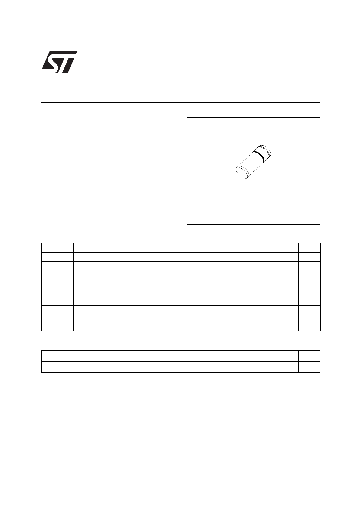
TMMBAT 43
MINIMELF
(Glass)
Symbol Parameter Value Unit
V
I
FRM
I
FSM
P
T
RRM
I
F
tot
stg
T
T
L
Repetitive Peak Reverse Voltage 30 V
Forward Continuous Current
Repetitive Peak Fordware Current tp ≤ 1s
Surge non Repetitive Forward Current tp = 10ms 4 A
Power Dissipation
Storage and Junction Temperature Range - 65 to 150
j
Maximum Temperature for Soldering during 15s 260
= 25
T
l
δ ≤
= 65 °C
T
l
0.5
C
°
200 mA
500 mA
200 mW
- 65 to 125
THERMAL RESIS TANCE
Symbol Test Conditions Value Unit
R
th(j-l)
Junction-leads 300
°
°
°
C/W
°
C
C
C
August 1999 Ed: 1A
1/4
TMMBAT 42/TMMBAT 43
ELECTRICAL CHARACT E RISTI CS
STATIC CHARACTERISTICS
Symbol Test Conditions Min. Typ. Max. Unit
V
BR
*
V
F
I
*
R
Tj = 25°CI
= 25°C
T
j
= 25°C
T
j
T
= 25°C
j
T
= 25°C
j
T
= 25°C
j
= 25°C
T
j
T
= 100°C
j
= 100µA
R
I
= 200mA All Types 1 V
F
I
= 10mA BAT 42 0.4
F
I
= 50mA 0.65
F
I
= 2mA BAT 43 0.26 0.33
F
I
= 15mA 0.45
F
V
= 25V 0.5
R
DYNAMIC CHARACT ERIS TICS
Symbol Test Conditions Min. Typ. Max. Unit
C
trr
η
= 25°CVR = 1V f = 1MHz
T
j
Tj = 25°CI
= 25°CRL = 15KΩCL = 300pF f = 45MHz Vi = 2V
T
j
= 10mA IR = 10mA i
F
= 1mA RL = 100
rr
30 V
7pF
Ω
80 %
100
5ns
A
µ
* Pulse t est: t
300µs δ < 2%
≤
p
.
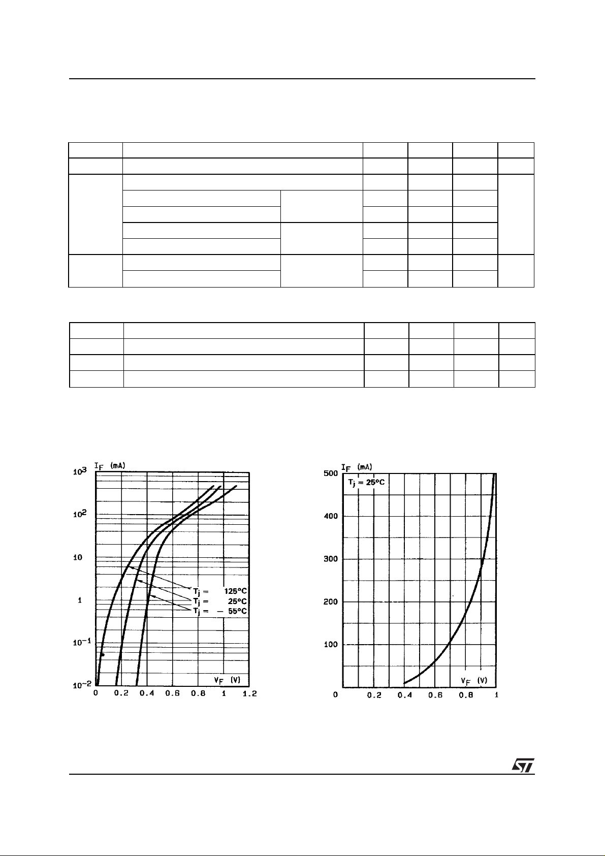
Figure 1. Forward current versus forward
voltage at different temperatures (typical
values).
Figure 2. Forward current versus forward
voltage (typical values).
2/4

TMMBAT 42/TMM BAT 43
Figure 3. Reverse current versus junction
temperature.
Figure 4. Rever se current versus continuous
reverse voltage (typical values).
Figure 5. Forward current versus forward
voltage (typical values).
3/4
TMMBAT 42/TMMBAT 43
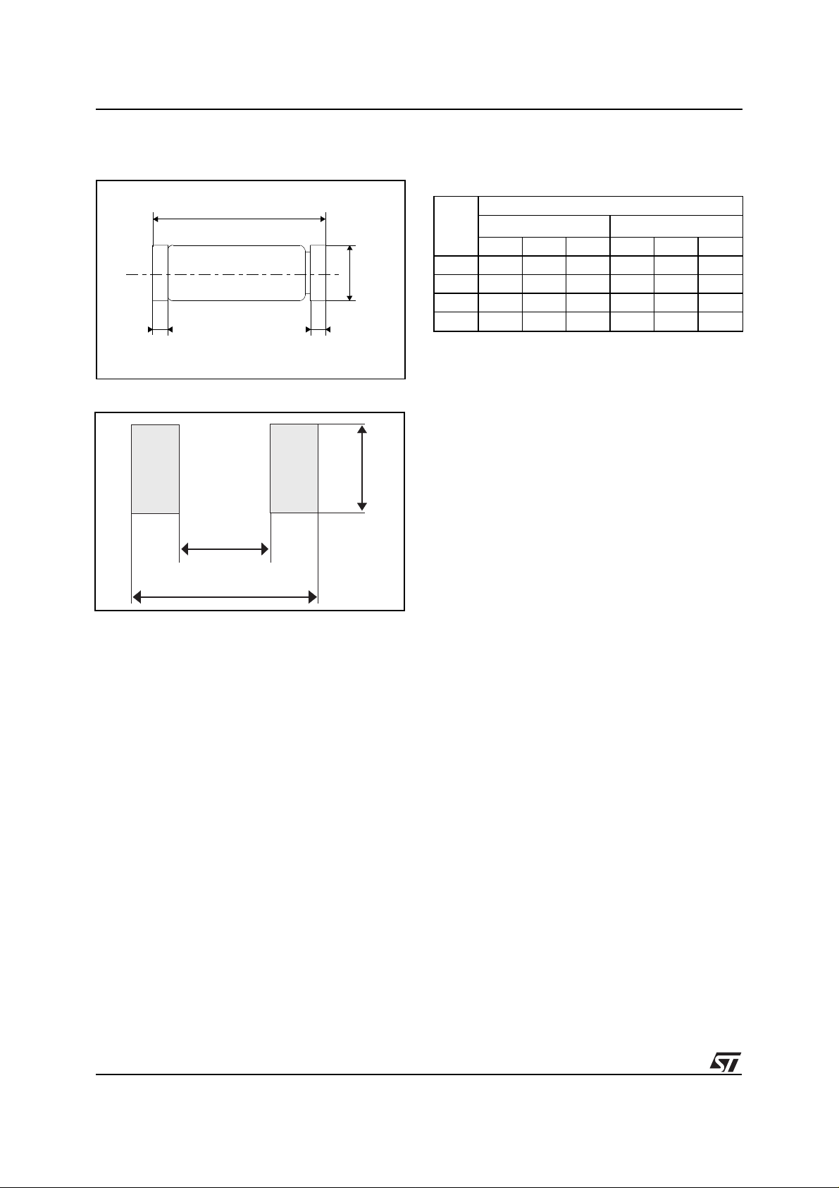
PACKAGE MECH ANICAL DATA
MINIMELF Glass
A
C
C
FOOT PRINT DIMENSIONS (Millimeter)
2.5
5
DIMENSIONS
REF.
Millimeters Inches
Min. T yp. Max. Min. T yp. Max.
B
/
O
A 3.30 3.40 3.6 0.130 0.134 0.142
B 1.59 1.60 1.62 0.063 0.063 0.064
C 0.40 0.45 0.50 0.016 0.018 0.020
D 1.50 0.059
2
Marking: ring at cathode end.
Weight: 0.05g
Information furnished is believed to be accurate and reliable. However, STMicroelectronics assumes no responsibility for the consequences of
use of such information nor for any infri ngem ent of patents or other rights of third parties which may result from its use. No license i s grant ed
by implication or otherwise under any patent or patent rights of STMicroelectronics. Specifications mentioned in this publication ar e sub j ect to
change without notice. This publication supersedes and replaces all information previously supplied.
STMicroelectronics products are not authorized for use as critical components in life support devices or systems without express written approval
of STMicroelectronic s.
The ST logo is a registered trademark of STMicroelectronics
© 1999 STMicroelectronics - Printed in Italy - All rights reserved.
STMicroelectronics GROUP OF COMPANIES
Australia - Brazil - China - Finland - France - Germany - Hong Kong - India - Italy - Japan - Malaysia
Malta - Morocco - Singapore - Spain - Sweden - Switzerland - United Kingdom - U.S.A.
http://www.st.com
4/4
 Loading...