

Features
■ It can work in two different power supply
modes:
– External power mode of 5 V
– Battery powered mode (Li -Ion battery
inside)
■ Hardware content:
– One mother board
– One daughter board with STCF03 and
power LED
– GUI installation file with all PC driver and
PC GUI
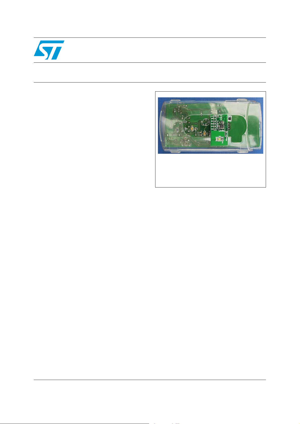
Description
The STEVAL-TLL005V1 is a power flash
demonstration board based on the STCF03. The
STCF03 is a high efficiency power supply solution
to drive a single flash LED in camera phone,
PDAs and other hand-held devices. It is a buckboost converter to guarantee a proper LED
current control over all possible conditions of
battery voltage and output voltage. All the
functions of the device are controlled through I
interface with microcontroller. The STEVALTLL005V1 include a mother plus a daughter
(STEVAL-TLL004V1 is the daughter only) boards.
2
C
STEVAL-TLL005V1
Power flash demonstration board
based on the STCF03 and ST7
Data Brief
STEVAL-TLL005V1
November 2008 Rev 1 1/4
For further information contact your local STMicroelectronics sales office.
www.st.com
4
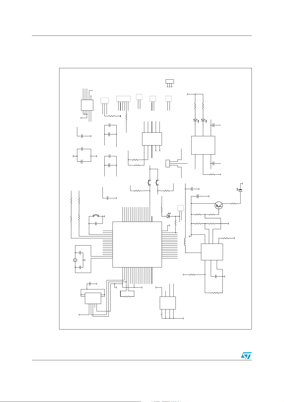
Electrical schematic STEVAL-TLL005V1
1 Electrical schematic
Figure 1. STCF03 driver board
123
FOR BAT
CON3
PF6
PF5
RESET
VppVDD
10
2
6
8
VDD
VDD
R3
SDA
R1
XT1
VDDF
VDD
4.7kR44.7k
SCL
100
R2
12MHz
USB_5V
4
4
2
6
8
1
10
P1
1
3
5
7
9
ICC
H1
1
3
5
7
9
VDD
PROX
GND
OSC1
220nF
C10
GND
C6
100nF
C5
100
C2
33pF
C1
33pF
7
6
GND
10uF
Tantale
VDD VDD
USBVCC
SW1
RESET
C3
10nF
GND
0.1uF
C17
GND
J1
SHD
SHD
SHD
VBUS1D-2D+3ID
9
SHD
8
GND
5
4
123
H2
2
3
PROX_SENSOR
GND
SDA_D
SCL_D
TRIG
GND
10k
R22
GND
C8
100nF
C12
4.7uF
Tantale
(pin #62)
GND
(pin #59)
C7
100nF
C11
4.7uF
Tantale
GND
(pin #31)
(pin #32)
C4
47nF
GND
GND
Vpp
RESET
PF5
PF6
VDD
VDD
GND
GND
OSC1
OSC2
48
47
PE3
PE4
49
Vpp
50
RESET
51
PF0
52
PF1
53
PF2
54
PF3
55
PF4
56
PF5
57
PF6
58
Vdd2
59
Vdda
60
Vssa
61
Vss2
62
OSCIN
63
OSCOUT
64
USBVss1USBDM
U1
2
USBDM
GND
GND
1
2
H4
4
5
6
ATN
GND
R20
10k
VDDF
VDDF
PE0
45
46
PE1 (HS)
PE2 (HS)
PE0 (HS)
USBDP
USBVCC4USBVdd
3
USBVCC
USBDP
R5
1.5k
EXT_SUPPLY
1
2
1
FLASH
DB BATTERY
SWITCH_2
2
H5
VBAT
GND
GND
6
GND
ST2329
NC
5
3
2
1
J2
CON3
R7
10k
VDD
R21
500
D4
GND
GND
Vss1
32
Vdd1
31
PC3 / MS_CLK
30
PC2 / MS_DAT
29
PC1 / MS_BS
28
PC0
27
PA7
26
PA6
25
PA5 / CF_WE
24
PA4 / SMC_R/B
23
PA3/SMC_RE/CF_RE
22
PA2/SMC_ALE/CF_A2
21
PA1/SMC_WE/CF_A1
20
PA0/SMC_CLE/CF_A0
19
PB7 / D7
18
PB6 / D6
17
SCL
6
7
SCL
VDD8nWC
E0
E12E2
U4
3
1
DB MAIN
R24
VDD
44
43
42
PD6
PD7
PD5
Vddf
Vssf
6
5
7
VDD
VDDF
GND
4.7k
R23
R6
ST72F651AR6T1E
V_EXT
4.7k
10k
PD441PD340PD2
PE5 / MMC_CMD8PE6 / MMC_DAT9PE7 / MMC_CLK
H3
GND
VDD
GND
VDDF
VDD
SDA
SCL
9
10
7
VL
VCC
IOVCC18IOVCC2
U5
IOVL1
OE3NC
IOVL2
2
4
1
SDA_D
SCL_D
VDDF
GND
S1 PROX_TRIG
S2
PROX
36
35
33
39
37
PC7
PC534PC4
PC6
PD138PD0
PB2 / D2
PB0 / D011PB1 / D1
PB3 / D3
PB4 / D415PB5 / D5
14
10
13
16
12
VDD
GND
BATTERY
VDDF
R11
SDA
5
SDA
VSS
4
USB_5V
R14
220
R15
220
C16
D1
3
CHRG
VBAT_OUTV_EXT
1
J3
PIR_EN
GND
PE0
10k
VDD
SWITCH_2
ATN
TRIG
M24C02
GND4PROG
U3
VDD
GND
C14
47uF/16V
VBAT
+
GND
+
C13
47uF/16V
2
L1
VBAT
200k
R13
33k
R12
VBAT_OUT
10uH
7
U2
R10
18k
GND
4.7uF
D2
VBATUSB_5VR19
2
1
BAT
POWER ON
VCC
STBC08
5
6
GND GND
C15
1uF
5k
GND
GND
Q1
2STR2215
R9
10k
12k
R17
5
8
3
1
FB
LBO
OUT
LX
2
SHDN
GND
REF
LBI
4
6
100nF
C9
R16
16k
STCF03 driver board schematic
GND
LED
D3
R18
1k
GND
R8
10k
VBAT_OUT
L6920
GND
AM01303v1
2/4

STEVAL-TLL005V1 Revision history
2 Revision history
Table 1. Document revision history
Date Revision Changes
27-Nov-2008 1 Initial release.
3/4

STEVAL-TLL005V1
y
Please Read Carefully:
Information in this document is provided solely in connection with ST products. STMicroelectronics NV and its subsidiaries (“ST”) reserve the
right to make changes, corrections, modifications or improvements, to this document, and the products and services described herein at any
time, without notice.
All ST products are sold pursuant to ST’s terms and conditions of sale.
Purchasers are solely responsible for the choice, selection and use of the ST products and services described herein, and ST assumes no
liability whatsoever relating to the choice, selection or use of the ST products and services described herein.
No license, express or implied, by estoppel or otherwise, to any intellectual property rights is granted under this document. If any part of this
document refers to any third party products or services it shall not be deemed a license grant by ST for the use of such third party products
or services, or any intellectual property contained therein or considered as a warranty covering the use in any manner whatsoever of such
third party products or services or any intellectual property contained therein.
UNLESS OTHERWISE SET FORTH IN ST’S TERMS AND CONDITIONS OF SALE ST DISCLAIMS ANY EXPRESS OR IMPLIED
WARRANTY WITH RESPECT TO THE USE AND/OR SALE OF ST PRODUCTS INCLUDING WITHOUT LIMITATION IMPLIED
WARRANTIES OF MERCHANTABILITY, FITNESS FOR A PARTICULAR PURPOSE (AND THEIR EQUIVALENTS UNDER THE LAWS
OF ANY JURISDICTION), OR INFRINGEMENT OF ANY PATENT, COPYRIGHT OR OTHER INTELLECTUAL PROPERTY RIGHT.
UNLESS EXPRESSLY APPROVED IN WRITING BY AN AUTHORIZED ST REPRESENTATIVE, ST PRODUCTS ARE NOT
RECOMMENDED, AUTHORIZED OR WARRANTED FOR USE IN MILITARY, AIR CRAFT, SPACE, LIFE SAVING, OR LIFE SUSTAINING
APPLICATIONS, NOR IN PRODUCTS OR SYSTEMS WHERE FAILURE OR MALFUNCTION MAY RESULT IN PERSONAL INJURY,
DEATH, OR SEVERE PROPERTY OR ENVIRONMENTAL DAMAGE. ST PRODUCTS WHICH ARE NOT SPECIFIED AS "AUTOMOTIVE
GRADE" MAY ONLY BE USED IN AUTOMOTIVE APPLICATIONS AT USER’S OWN RISK.
Resale of ST products with provisions different from the statements and/or technical features set forth in this document shall immediately void
any warranty granted by ST for the ST product or service described herein and shall not create or extend in any manner whatsoever, an
liability of ST.
ST and the ST logo are trademarks or registered trademarks of ST in various countries.
Information in this document supersedes and replaces all information previously supplied.
The ST logo is a registered trademark of STMicroelectronics. All other names are the property of their respective owners.
© 2008 STMicroelectronics - All rights reserved
STMicroelectronics group of companies
Australia - Belgium - Brazil - Canada - China - Czech Republic - Finland - France - Germany - Hong Kong - India - Israel - Italy - Japan -
Malaysia - Malta - Morocco - Singapore - Spain - Sweden - Switzerland - United Kingdom - United States of America
www.st.com
4/4
 Loading...