

Features
■ Adjustable output voltage: 2.5 to 36 V
■ Sink current capability: 1 to 100 mA
■ Typical output impedance: 0.22 Ω
■ 1% and 2% voltage precision
■ Automotive temp. range - 40 °C to +125 °C
Applications
■ Power supply
■ Industrial
■ Automotive
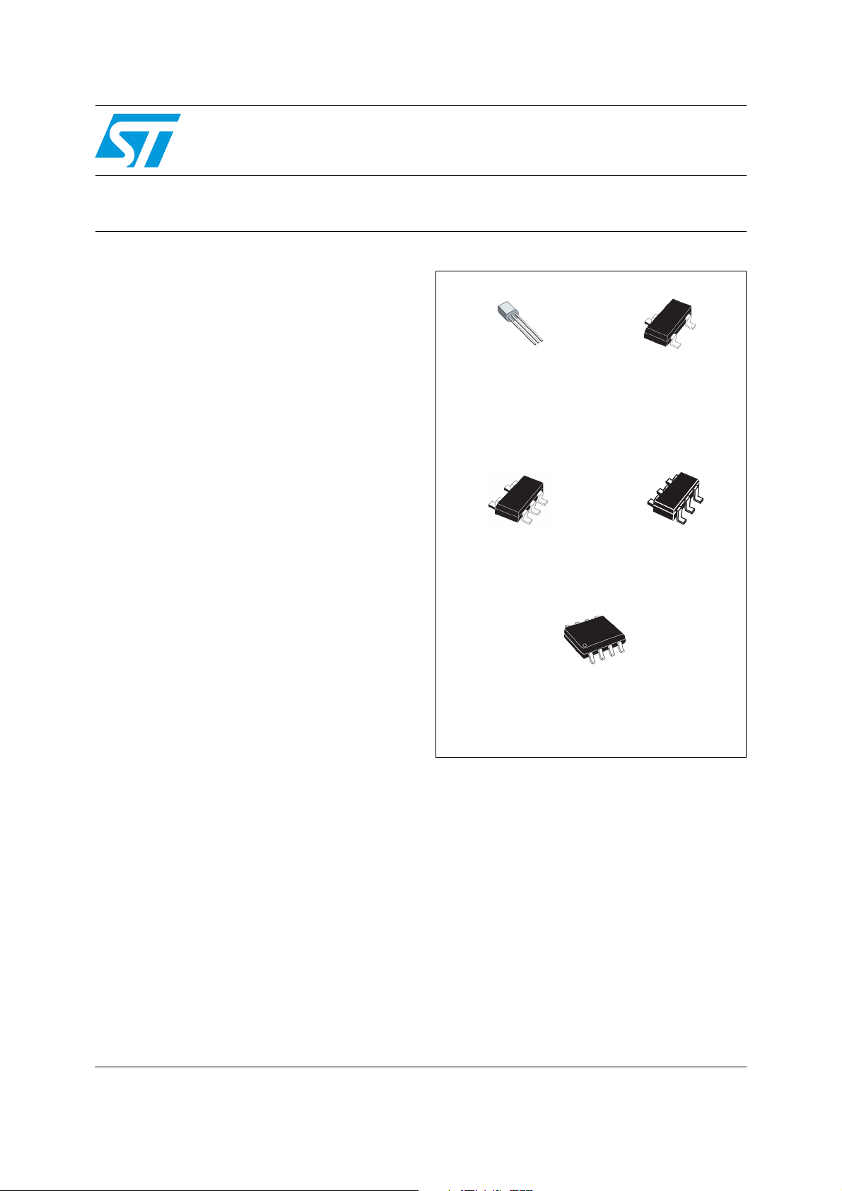
TL431
TL432
Programmable voltage reference
Z
TO-92
(Plastic package)
L
SOT23-3
Description
The TL431 and TL432 are programmable shunt
voltage references with guaranteed temperature
stability over the entire operating temperature
range. The device temperature range is extended
for the automotive version from -40 °C up to
+125 °C. The output voltage can be set to any
value between 2.5 and 36 V with two external
resistors. The TL431 and TL432 operate with a
wide current range from 1 to 100 mA with a typical
dynamic impedance of 0.22 Ω.
L
SOT23-5
D
SO-8
(Batwing plastic micropackage)
C
SOT323-6
November 2011 Doc ID 4467 Rev 10 1/21
www.st.com
21

Contents TL431, TL432
Contents
1 Schematic diagrams . . . . . . . . . . . . . . . . . . . . . . . . . . . . . . . . . . . . . . . . . 3
2 Absolute maximum ratings and operating conditions . . . . . . . . . . . . . 4
3 Electrical characteristics . . . . . . . . . . . . . . . . . . . . . . . . . . . . . . . . . . . . . 5
3.1 Reference input voltage deviation over temperature range . . . . . . . . . . . . 7
4 Package information . . . . . . . . . . . . . . . . . . . . . . . . . . . . . . . . . . . . . . . . 11
4.1 SO-8 package information . . . . . . . . . . . . . . . . . . . . . . . . . . . . . . . . . . . . 12
4.2 TO-92 ammopack and tape and reel package information . . . . . . . . . . . 13
4.3 TO-92 (bulk) package information . . . . . . . . . . . . . . . . . . . . . . . . . . . . . . 14
4.4 SOT23-3 package information . . . . . . . . . . . . . . . . . . . . . . . . . . . . . . . . . 15
4.5 SOT23-5 package information . . . . . . . . . . . . . . . . . . . . . . . . . . . . . . . . . 16
4.6 SOT323-6 package information . . . . . . . . . . . . . . . . . . . . . . . . . . . . . . . . 17
5 Ordering information . . . . . . . . . . . . . . . . . . . . . . . . . . . . . . . . . . . . . . . 18
6 Revision history . . . . . . . . . . . . . . . . . . . . . . . . . . . . . . . . . . . . . . . . . . . 20
2/21 Doc ID 4467 Rev 10
TL431, TL432 Schematic diagrams
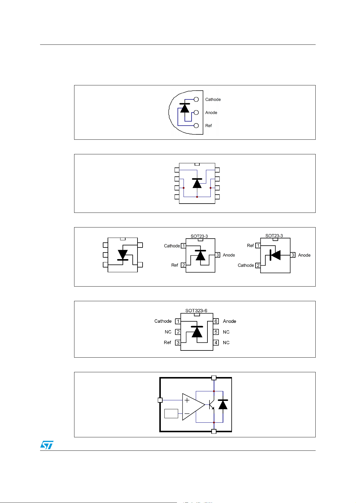
1 Schematic diagrams
Figure 1. TO-92 pin connections (top view)
Figure 2. SO-8 batwing pin connections (top view)
SO8
Cathode Ref1
Anode
NC
2
3
4
8
7
6
Anode
NC5
Figure 3. SOT23-5 and SOT23-3 pin connections (top view)
SOT23-3SOT23-5
NC
NC
2
Cathode Ref
34
TL431
Figure 4.
SOT323-6 pin connections (top view)
Anode1
5 Cathode
Ref Anode
1
23
TL431
Figure 5. TL431 and TL432 block diagram
Cathode
Ref
TL432
Vref
Anode
Doc ID 4467 Rev 10 3/21

Absolute maximum ratings and operating conditions TL431, TL432
2 Absolute maximum ratings and operating conditions
Table 1. Absolute maximum ratings
Symbol Parameter Value Unit
V
R
R
T
ESD
1. Short-circuits can cause excessive heating. These values are typical.
2. Human body model: a 100 pF capacitor is charged to the specified voltage, then discharged through a
3. Machine model: a 200 pF capacitor is charged to the specified voltage, then discharged directly between
4. Charged device model: all pins and the package are charged together to the specified voltage and then
Table 2. Operating conditions
Cathode to anode voltage 37 V
KA
I
Continuous cathode current range -100 to +150 mA
k
Reference input current range -0.05 to +10 mA
I
ref
(1)
(1)
(2)
200
85
248
157
221
30
136
67
110
3000
2000
200
1500
°C/W
°C/W
Thermal resistance junction to ambient
TO-92
SO-8 batwing
thja
SOT23-3L
SOT23-5L
SOT323-6L
Thermal resistance junction to case
SO-8 batwing
SOT23-3L
thjc
SOT23-5L
SOT323-6L
Storage temperature range -65 to +150 °C
stg
Junction temperature 150 °C
T
J
TL431IY, TL431AIY-T: HBM (human body model)
TL431-TL432: HBM (human body model)
MM: machine model
CDM: charged device model
1.5 kΩ resistor between two pins of the device. This is done for all couples of connected pin combinations
while the other pins are floating.
two pins of the device with no external series resistor (internal resistor < 5 Ω). This is done for all couples of
connected pin combinations while the other pins are floating.
discharged directly to the ground through only one pin. This is done for all pins.
(3)
(4)
V
Symbol Parameter Value Unit
V
Cathode to anode voltage V
KA
Cathode current 1 to 100 mA
I
k
Operating free-air temperature range
T
TL431C/AC
oper
TL431I/AI - TL432I/AI
TL431IY/AIY
4/21 Doc ID 4467 Rev 10
to 36 V
ref
0 to +70
-40 to +105
-40 to +125
°C

TL431, TL432 Electrical characteristics
3 Electrical characteristics
Table 3. TL431C: 0° C to 70° C (T
= 25° C unless otherwise specified)
amb
TL431C TL431AC
Symbol Parameter
Min. Typ. Max. Min. Typ. Max.
Reference input voltage
V
ref
= V
V
KA
T
min
, Ik = 10 mA, T
ref
≤ T
amb
≤ T
max
amb
=25°C
2.44
2.423
2.495 2.55
Reference input voltage deviation over temperature
ΔV
ref
range
VKA = V
(1)
, Ik = 10 mA, T
ref
min
≤ T
amb
≤ T
max
317 315
Ratio of change in reference input voltage to change
ΔVref
------------
ΔVka
in cathode to anode voltage
= 10 mA - ΔVKA = 10 V to V
I
k
= 36 V to 10 V
ΔV
KA
ref
-2.7-2-1.4
-1
Reference input current
Ik = 10 mA, R1 = 10 kΩ, R2 = ∞
I
ref
T
T
amb
min
= 25° C
≤ T
amb
≤ T
1.8 4
max
Reference input current deviation over temperature
ΔI
I
⏐ZKA⏐
1. See definition of Section 3.1: Reference input voltage deviation over temperature range.
2. The dynamic impedance is defined as
range
ref
= 10 mA, R1 = 10 kΩ, R2 =∞
I
k
T
min
≤ T
amb
≤ T
max
0.4 1.2 0.4 1.2
Minimum cathode current for regulation
min
I
off
= V
V
KA
ref
0.5 1 0.5 0.6
Off-state cathode current 2.6 1000 2.6 1000 nA
Dynamic impedance
VKA = V
, Δ Ik = 1 to 100 mA, f ≤ 1 kHZ 0.22 0.5 0.22 0.5
ref
(2)
|ZKA|
ΔV
KA
=
--------------- -
IkΔ
2.567
5.2
2.47
2.495 2.52
2.453
-2.7-2-1.4
2.537
-1
1.8 4
5.2
Unit
V
mV
mV/V
µA
µA
mA
Ω
Doc ID 4467 Rev 10 5/21

Electrical characteristics TL431, TL432
Table 4. TL431I/TL432I: -40° C to 105° C, T
= 25°C (unless otherwise specified)
amb
TL431I/TL432I TL431AI/TL432AI
Symbol Parameter
Min. Typ. Max. Min. Typ. Max.
Reference input voltage
V
ΔV
ref
ref
VKA = V
T
min
Reference input voltage deviation over temperature
range
VKA = V
, Ik = 10 mA, T
ref
≤ T
amb
(1)
, Ik =10 mA, T
ref
≤ T
max
amb
min
= 25° C
≤ T
amb
≤ T
max
2.44
2.41
2.495 2.55
2.58
730 730mV
Ratio of change in reference input voltage to change
ΔVref
------------
ΔVka
in cathode to anode voltage
= 10 mA, ΔVKA = 10 V to V
I
k
= 36 V to 10 V
ΔV
KA
ref
-2.7-2-1.4
-1
Reference input current
Ik = 10 mA, R1 = 10 kΩ, R2 = ∞
I
ref
T
T
amb
min
= 25° C
≤ T
amb
≤ T
max
1.8 4
6.5
Reference input current deviation over temperature
ΔI
I
⏐ZKA⏐
1. See definition of Section 3.1: Reference input voltage deviation over temperature range below.
2. The dynamic impedance is defined as
range
min
I
off
ref
= 10 mA, R1 = 10 kΩ, R2 = ∞
I
k
T
min
≤ T
amb
≤ T
max
Minimum cathode current for regulation
VKA = V
ref
0.8 2.5 0.8 1.2 µA
0.5 1 0.5 0.7 mA
Off-state cathode current 2.6 1000 2.6 1000 nA
(2)
Dynamic impedance
= V
V
KA
, Δ Ik = 1 to 100 mA, f ≤ 1kHZ
ref
ΔV
|ZKA|
KA
=
--------------- -
IkΔ
0.22 0.5 0.22 0.5 Ω
2.47
2.495 2.52
2.44
-2.7-2-1.4
-1
1.8 4
2.55
6.5
Unit
V
mV/V
µA
6/21 Doc ID 4467 Rev 10
TL431, TL432 Electrical characteristics
Table 5. TL431IY: -40° C to 125° C, T
= 25°C (unless otherwise specified)
amb
TL431IY TL431AIY
Symbol Parameter
Min. Typ. Max. Min. Typ. Max.
Reference input voltage
V
ΔV
ref
ref
VKA = V
T
min
Reference input voltage deviation over temperature
range
VKA = V
, Ik = 10 mA
ref
≤ T
amb
(1)
, Ik = 10 mA, T
ref
≤ T
max
min
≤ T
amb
≤ T
max
2.44
2.41
2.495 2.55
2.58
730 730mV
Ratio of change in reference input voltage to change
ΔVref
------------
ΔVka
in cathode to anode voltage
= 10 mA, ΔVKA = 10 V to V
I
k
= 10 mA, ΔVKA = 36 V to 10 V
I
k
ref
-2.7-2-1.4
-1
Reference input current
Ik = 10 mA, R1 = 10 kΩ, R2 = ∞
I
ref
≤ T
T
min
amb
≤ T
max
1.8 4
6.5
Reference input current deviation over temperature
ΔI
I
⏐ZKA⏐
1. See definition of Section 3.1: Reference input voltage deviation over temperature range below.
2. The dynamic impedance is defined as
range
ref
= 10 mA, R1 = 10 kΩ, R2 = ∞, T
I
k
T
max
Minimum cathode current for regulation
min
I
off
= V
V
KA
ref
Off-state cathode current
≤ T
T
min
Dynamic impedance
= V
V
KA
≤ T
amb
ref
max
(2)
, Δ Ik = 1 to 100 mA, F ≤ 1kHz
min
≤ T
amb
≤
0.8 2.5 0.8 1.2 µA
0.5 1 0.5 0.6 mA
2.6 1000
3000
ΔV
|ZKA|
KA
=
--------------- -
IkΔ
0.22 0.5 0.22 0.5 Ω
2.47
2.495 2.52
2.44
-2.7-2-1.4
-1
1.8 4
2.6 1000
Unit
V
2.55
mV/V
µA
6.5
nA
3000
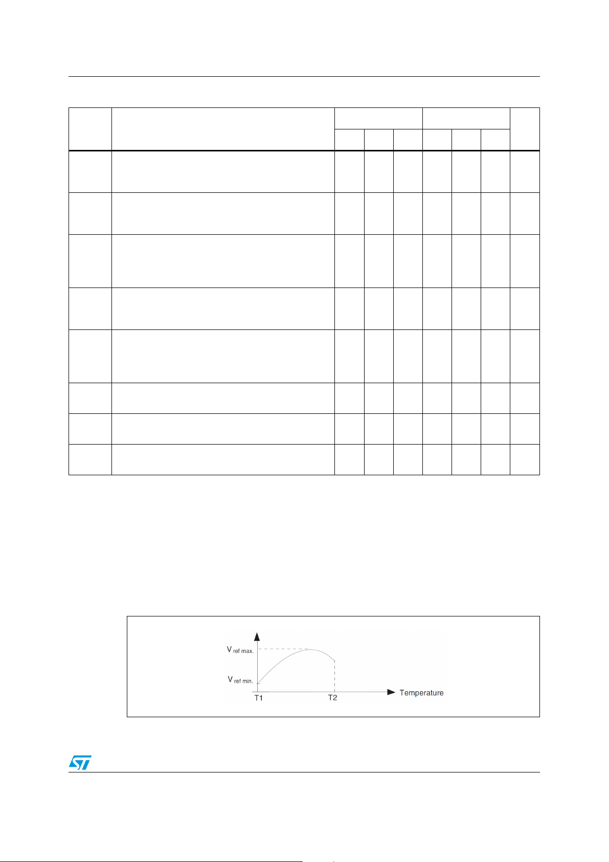
3.1 Reference input voltage deviation over temperature range
Δ
V
is defined as the difference between the maximum and minimum values obtained over
ref
the full temperature range.
Δ
V
= V
ref
Figure 6. Reference input voltage deviation over temperature range
ref max
- V
ref min
Doc ID 4467 Rev 10 7/21
 Loading...