

ST TL084 User Manual
General purpose JFET quad operational amplifiers
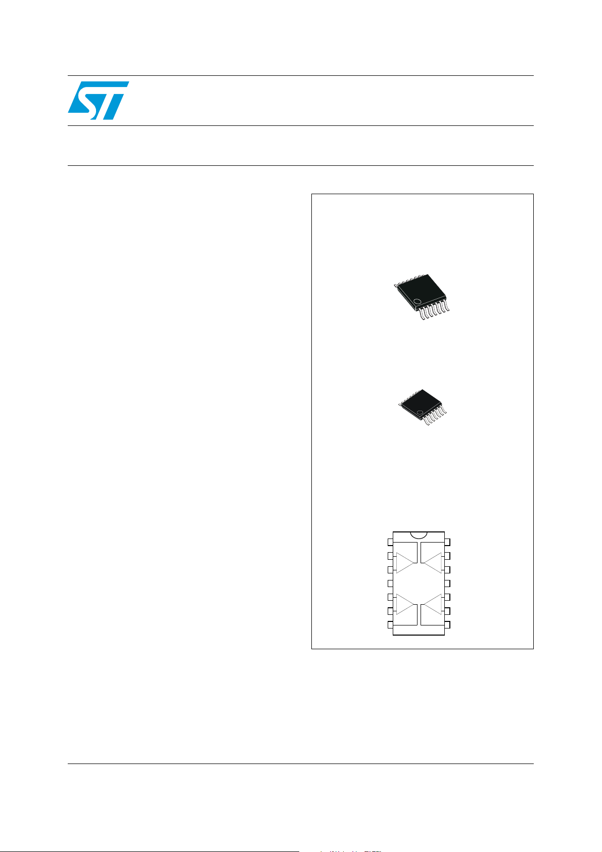
D
TSSOP-14
(Thin shrink small outline package)
N
DIP14
(Plastic package)
D
SO-14
(Plastic micropackage)
Pin connections
(Top view)
Inverting Input 2
Non-inverting Input 2
Non-inverting Input 1
CC
V
-
CC
V
1
2
3
4
8
5
6
7
9
10
11
12
13
14
+
Output 3
Output 4
Non-inverting Input 4
Inverting Input 4
Non-inverting Input 3
Inverting Input 3
-
+
-
+
-
+
-
+
Output 1
Inverting Input 1
Output 2
Features
■ Wide common-mode (up to V
differential voltage range
■ Low input bias and offset current
■ Output short-circuit protection
■ High input impedance JFET input stage
■ Internal frequency compensation
■ Latch up free operation
■ High slew rate: 16 V/µs (typical)
Description
The TL084, TL084A and TL084B are high-speed
JFET input quad operational amplifiers
incorporating well matched, high voltage JFET
and bipolar transistors in a monolithic integrated
circuit.
The devices feature high slew rates, low input
bias and offset currents, and low offset voltage
temperature coefficient.
CC
+
) and
TL084
Datasheet — production data
July 2012 Doc ID 2301 Rev 4 1/20
This is information on a product in full production.
www.st.com
20

Schematic diagram TL084
Output
Non-inverting
input
Inverting
input
V
CC
V
CC
200
Ω
Ω
100
Ω
100
1.3k
30k
35k
35k
Ω
100
1.3k
8.2k
1 Schematic diagram
Figure 1. Circuit schematics (for each amplifier)
2/20 Doc ID 2301 Rev 4

TL084 Absolute maximum ratings and operating conditions
2 Absolute maximum ratings and operating conditions
Table 1. Absolute maximum ratings
Value
Symbol Parameter
V
V
V
R
Supply voltage
CC
Input voltage
in
Differential input voltage
id
Thermal resistance junction to ambient
(5)
thja
SO-14
(1)
(2)
DIP14
TSSOP14
Thermal resistance junction to
(4) (5)
case
R
thjc
SO-14
DIP14
TSSOP14
(3)
TL084I, AI, BI TL084C, AC, BC
±18 V
±15 V
±30 V
(4)
105
80
100
31
33
32
Unit
°C/W
°C/W
P
T
T
ESD
1. All voltage values, except differential voltage, are with respect to the zero reference level (ground) of the
supply voltages where the zero reference level is the midpoint between V
2. The magnitude of the input voltage must never exceed the magnitude of the supply voltage or 15 volts,
whichever is less.
3. Differential voltages are the non-inverting input terminal with respect to the inverting input terminal.
4. Short-circuits can cause excessive heating and destructive dissipation.
5. R
6. The output may be shorted to ground or to either supply. Temperature and/or supply voltages must be
limited to ensure that the dissipation rating is not exceeded.
7. Human body model: 100 pF discharged through a 1.5 kΩ resistor between two pins of the device, done for
all couples of pin combinations with other pins floating.
8. Machine model: a 200 pF cap is charged to the specified voltage, then discharged directly between two
pins of the device with no external series resistor (internal resistor < 5 Ω), done for all couples of pin
combinations with other pins floating.
9. Charged device model: all pins plus package are charged together to the specified voltage and then
discharged directly to the ground.
Power dissipation 680 mW
tot
(7)
(6)
(9)
Infinite
1000
150
1500
+
and V
CC
CC
-
.
Output short-circuit duration
Operating free-air temperature range -40 to +105 0 to +70 °C
oper
Storage temperature range -65 to +150 °C
stg
HBM: human body model
(8)
CDM: charged device model
are typical values.
th
VMM: machine model
Doc ID 2301 Rev 4 3/20

Absolute maximum ratings and operating conditions TL084
Table 2. Operating conditions
Symbol Parameter TL084I, AI, BI TL084C, AC, BC Unit
V
T
CC
oper
Supply voltage range 6 to 36 V
Operating free-air temperature range -40 to +105 0 to +70 °C
4/20 Doc ID 2301 Rev 4

TL084 Electrical characteristics
3 Electrical characteristics
Table 3. VCC = ±15V, T
= +25°C (unless otherwise specified)
amb
Symbol Parameter
Input offset voltage (Rs = 50Ω)
T
= +25°C TL084
amb
TL084A
V
io
TL084B
≤ T
T
min
amb
≤ T
max
TL084
TL084A
TL084B
DV
Input offset voltage drift 10 10 μV/°C
io
Input offset current
I
io
I
ib
T
= +25°C
amb
≤ T
T
min
amb
≤ T
Input bias current
T
= +25°C
amb
≤ T
T
min
amb
≤ T
max
(1)
max
Large signal voltage gain (RL = 2kΩ, Vo =±10V)
A
vd
T
T
amb
min
= +25°C
≤ T
amb
≤ T
max
Supply voltage rejection ratio (R
SVR
T
T
amb
min
= +25°C
≤ T
amb
≤ T
max
Supply current, no load
I
CC
V
icm
T
= +25°C
amb
≤ T
T
min
amb
≤ T
max
Input common mode voltage range
= 50Ω)
S
TL084I,AC,AI, BC,BI TL084C
Min. Typ. Max. Min. Typ. Max.
3
10
3
1
6
3
13
310
13
7
5
5100
51004pA
4
20 200
30 20020pA
20
5025200 2515200
80
80
±11 +15
86 70
1.4 2.5
2.5
±11 +15
-12
86 dB
70
1.4 2.5
2.5
-12
Unit
mV
nA
nA
V/mV
mA
V
CMR
I
os
±V
opp
SR
Common mode rejection ratio (R
= +25°C
T
amb
≤ T
T
min
amb
≤ T
max
= 50Ω)
S
Output short-circuit current
T
= +25°C
amb
T
≤ T
amb
≤ T
max
min
Output voltage swing
T
= +25°C RL = 2kΩ
amb
= 10kΩ
R
L
≤ T
T
R
min
L
amb
= 10kΩ
≤ T
RL = 2kΩ
max
Slew rate
V
= 10V, RL = 2kΩ, CL = 100pF, unity gain
in
80
80
10
10
10
12
10
12
86 70
40 60
60
12
13.5
70
10
10
10
12
10
12
86
40 60
60
12
13.5
dB
mA
V
816 816 V/μs
Doc ID 2301 Rev 4 5/20

Electrical characteristics TL084
nV
Hz
------------
Table 3. VCC = ±15V, T
= +25°C (unless otherwise specified) (continued)
amb
TL084I,AC,AI, BC,BI TL084C
Symbol Parameter
Min. Typ. Max. Min. Typ. Max.
Rise time
t
r
K
ov
GBP
R
Vin = 20mV, RL = 2kΩ, CL = 100pF, unity gain
Overshoot
Vin = 20mV, RL = 2kΩ, CL = 100pF, unity gain
Gain bandwidth product
V
= 10mV, RL = 2kΩ, CL = 100pF, F= 100kHz
in
Input resistance 10
i
2.5 4 2.5 4 MHz
0.1 0.1 μs
10 10 %
12
10
12
Total harmonic distortion
THD
e
n
F= 1kHz, R
= 2Vpp)
V
o
Equivalent input noise voltage
RS = 100Ω, F= 1kHz
= 2kΩ,CL = 100pF, Av = 20dB,
L
∅m Phase margin 45 45
Vo1/V
1. The input bias currents are junction leakage currents which approximately double for every 10°C increase in the junction
temperature.
Channel separation
o2
A
= 100
v
0.01 0.01 %
15 15
degrees
120 120 dB
Unit
Ω
6/20 Doc ID 2301 Rev 4
 Loading...