

ST TL082, TL082A, TL082B User Manual
General purpose JFET dual operational amplifiers
Features
■ Wide common-mode (up to V
differential voltage range
■ Low input bias and offset current
■ Output short-circuit protection
■ High input impedance JFET input stage
■ Internal frequency compensation
■ Latch up free operation
■ High slew rate: 16 V/µs (typical)
Description
The TL082, TL082A and TL082B are high speed
JFET input dual operational amplifiers
incorporating well matched, high voltage JFET
and bipolar transistors in a monolithic integrated
circuit.
CC
+
) and
TL082
TL082A TL082B
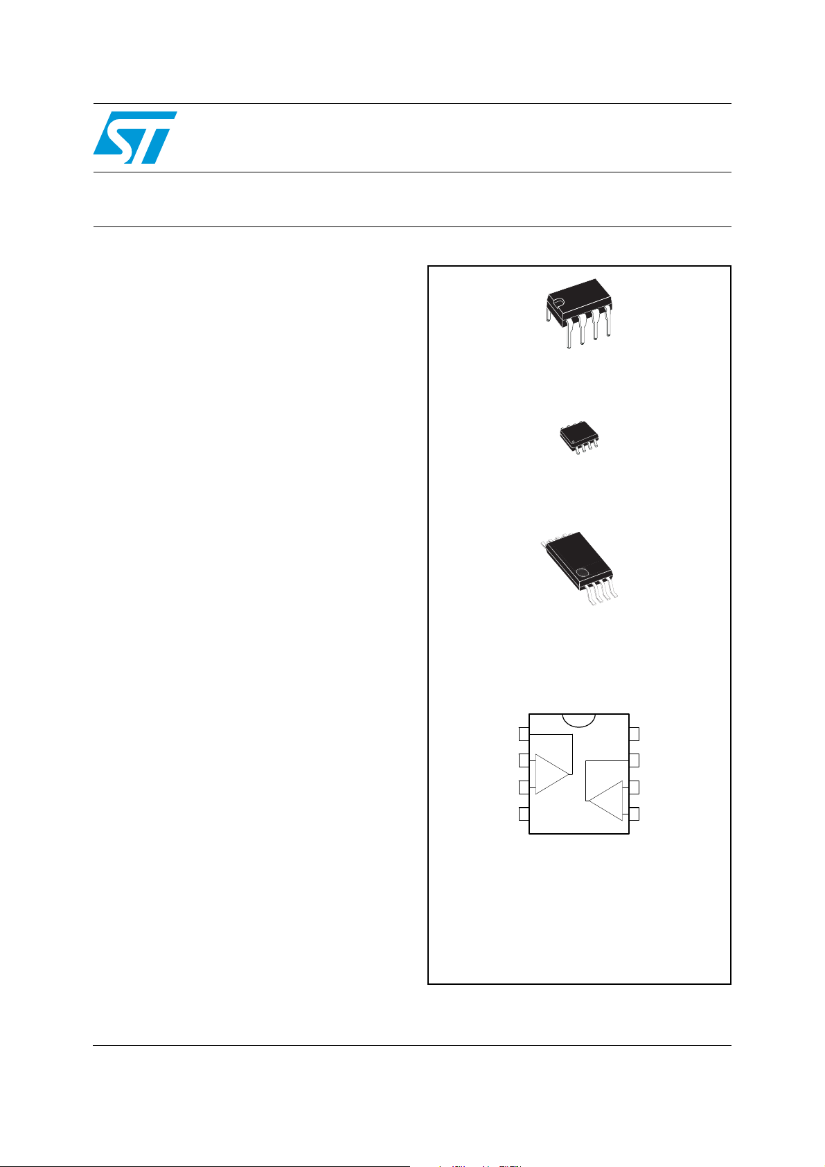
N
DIP8
(Plastic package)
D
SO-8
(Plastic micropackage)
The devices feature high slew rates, low input
bias and offset current, and low offset voltage
temperature coefficient.
P
TSSOP8
(Thin shrink small outline package)
Pin connections (top view)
1
2
-
+
3
45
8
7
6
-
+
1 - Output 1
2 - Inverting input 1
3 - Non-inverting input 1
4 - V
CC
-
5 - Non-inverting input 2
6 - Inverting input 2
7 - Output 2
8 - V
CC
+
June 2008 Rev 10 1/17
www.st.com
17
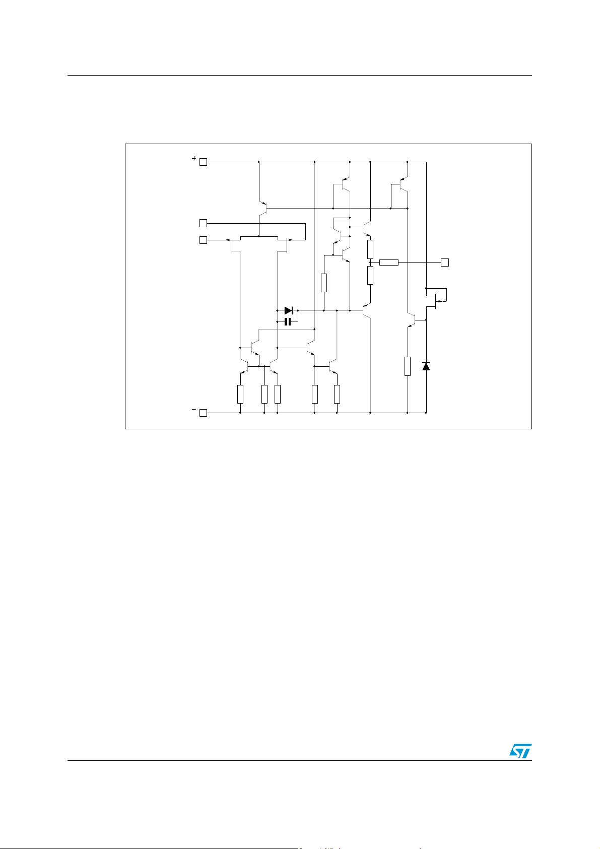
Schematic diagram TL082 TL082A TL082B
1 Schematic diagram
Figure 1. Schematic diagram
V
CC
Non-inverting
input
Inverting
input
30k
100
100
Ω
Ω
200
Ω
Output
1/2 TL082
8.2k
Ω
1.3k
35k
V
CC
1.3k
35k
100
2/17
TL082 TL082A TL082B Absolute maximum ratings and operating conditions
2 Absolute maximum ratings and operating conditions
Table 1. Absolute maximum ratings
Symbol Parameter
V
V
V
P
Supply voltage
CC
Input voltage
in
Differential input voltage
id
Power dissipation 680 mW
tot
(1)
(2)
(3)
Thermal resistance junction to ambient
R
thja
SO-8
DIP8
TSSOP8
Thermal resistance junction to case
R
thjc
SO-8
DIP8
TSSOP8
Output short-circuit duration
T
ESD
Storage temperature range -65 to +150 °C
stg
HBM: human body model
MM: machine model
(6)
(7)
CDM: charged device model
(5)
(8)
(4)
TL082I, AI, BITL082C, AC,
BC
±18 V
±15 V
±30 V
125
85
120
40
41
37
Infinite
1kV
200 V
1500 V
Unit
°C/W
°C/W
1. All voltage values, except differential voltage, are with respect to the zero reference level (ground) of the
supply voltages where the zero reference level is the midpoint between V
2. The magnitude of the input voltage must never exceed the magnitude of the supply voltage or 15 volts,
whichever is less.
3. Differential voltages are the non-inverting input terminal with respect to the inverting input terminal.
4. Short-circuits can cause excessive heating. Destructive dissipation can result from simultaneous short-
circuit on all amplifiers.
5. The output may be shorted to ground or to either supply. Temperature and/or supply voltages must be
limited to ensure that the dissipation rating is not exceeded
6. Human body model: 100 pF discharged through a 1.5 kΩ resistor between two pins of the device, done for
all couples of pin combinations with other pins floating.
7. Machine model: a 200 pF cap is charged to the specified voltage, then discharged directly between two
pins of the device with no external series resistor (internal resistor < 5 Ω), done for all couples of pin
combinations with other pins floating.
8. Charged device model: all pins plus package are charged together to the specified voltage and then
discharged directly to the ground.
Table 2. Operating conditions
CC
+
and V
CC
-
.
Symbol Parameter TL082I, AI, BI TL082C, AC, BC Unit
V
T
oper
Supply voltage 6 to 36 V
CC
Operating free-air temperature range -40 to +105 0 to +70 °C
3/17

Electrical characteristics TL082 TL082A TL082B
3 Electrical characteristics
Table 3. VCC = ±15V, T
= +25°C (unless otherwise specified)
amb
Symbol Parameter
Input offset voltage (Rs = 50Ω)
= +25°C TL082
T
amb
TL082A
V
io
T
≤ T
min
amb
≤ T
max
TL082B
TL082
TL082A
TL082B
DV
Input offset voltage drift 10 10 µV/°C
io
≤ T
max
(1)
Input offset current
I
io
T
T
amb
min
≤ T
= +25°C
amb
Input bias current
I
ib
T
T
amb
min
= +25°C
≤ T
amb
≤ T
max
Large signal voltage gain (RL = 2kΩ, Vo = ±10V)
A
vd
T
T
amb
min
= +25°C
≤ T
amb
≤ T
max
Supply voltage rejection ratio (R
SVR
T
T
amb
min
= +25°C
≤ T
amb
≤ T
max
Supply current, no load
I
CC
V
icm
T
= +25°C
amb
≤ T
T
min
amb
≤ T
max
Input common mode voltage range
= 50Ω)
S
TL082I,AC,AI,BC,
BI
TL082C
Min. Typ. Max. Min. Typ. Max.
3
10
3
6
1
3
13
310
13
7
5
5100
510010pA
4
20 200
20
20 400
20
5025200 2515200
808086 707086
1.4 2.5
±11 +15
-12
2.5
±11 +15
1.4 2.5
2.5
-12
Unit
mV
nA
pA
nA
V/mV
dB
mA
V
Common mode rejection ratio (RS = 50Ω)
CMR
T
T
amb
min
= +25°C
≤ T
amb
≤ T
max
Output short-circuit current
I
os
T
T
amb
min
= +25°C
≤ T
amb
≤ T
max
Output voltage swing
= +25°C RL = 2kΩ
T
T
amb
min
≤ T
amb
≤ T
RL = 10kΩ
RL = 2kΩ
max
±V
opp
RL = 10kΩ
SR
Slew rate
V
= 10V, RL = 2kΩ, CL = 100pF, unity gain 8 16 8 16 V/µs
in
4/17
808086 707086
101040 6060101040 60
60
10
12
10
12
12
13.5
10
12
10
12
12
13.5
dB
mA
V
TL082 TL082A TL082B Electrical characteristics
Table 3. VCC = ±15V, T
Symbol Parameter
= +25°C (unless otherwise specified) (continued)
amb
TL082I,AC,AI,BC,
BI
TL082C
Unit
Min. Typ. Max. Min. Typ. Max.
Rise time
t
r
K
ov
GBP
R
THD
e
n
i
Vin = 20mV, RL = 2kΩ, CL = 100pF, unity gain 0.1 0.1 µs
Overshoot
Vin = 20mV, RL = 2kΩ, CL = 100pF, unity gain 10 10 %
Gain bandwidth product
V
= 10mV, RL = 2kΩ, CL = 100pF, F= 100kHz 2.5 4 2.5 4 MHz
in
Input resistance 10
12
10
12
Total harmonic distortion
F=1kHz, R
= 2kΩ,CL=100pF, Av=20dB, Vo=2V
L
pp
0.01 0.01 %
Equivalent input noise voltage
= 100Ω, F = 1kHz 15 15
R
S
nV
------------
∅m Phase margin 45 45 degrees
Vo1/V
1. The input bias currents are junction leakage currents which approximately double for every 10° C increase in the junction
temperature.
Channel separation
o2
Av = 100
120 120 dB
Ω
Hz
5/17
Electrical characteristics TL082 TL082A TL082B
30
25
20
15
10
5
02468101214 16
MAXIMUM PEAK-TO-PEAK OUTPUT
VOLTAG E (V)
R
L
= 10 k
Ω
T
amb
= +25˚C
SUPPLY VOLTAGE ( V)
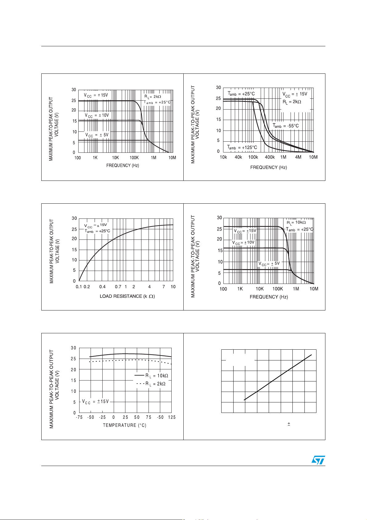
Figure 2. Maximum peak-to-peak output
voltage versus frequency
Figure 4. Maximum peak-to-peak output
voltage versus load resistance
Figure 3. Maximum peak-to-peak output
voltage versus frequency
Figure 5. Maximum peak-to-peak output
voltage versus frequency
Figure 6. Maximum peak-to-peak output
6/17
voltage versus free air temperature
Figure 7. Maximum peak-to-peak output
voltage versus supply voltage
 Loading...