

Low noise JFET dual operational amplifiers
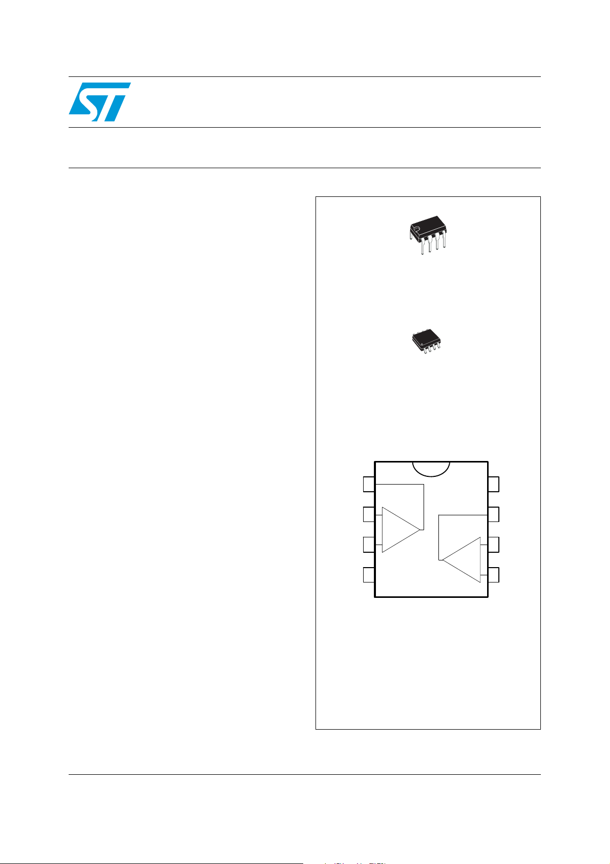
N
DIP8
(Plastic package)
D
SO-8
(Plastic micropackage)
1
2
3
45
6
7
8
-
+
-
+
Pin connections (top view)
1 - Output 1
2 - Inverting input 1
3 - Non-inverting input 1
4 - V
CC
-
5 - Non-inverting input 2
6 -Inverting input 2
7 - Output 2
8 - V
CC
+
Features
■ Wide common-mode (up to V
differential voltage range
■ Low input bias and offset current
■ Low noise e
■ Output short-circuit protection
■ High input impedance JFET input stage
■ Low harmonic distortion: 0.01% (typical)
■ Internal frequency compensation
■ Latch-up free operation
■ High slew rate: 16 V/µs (typ)
= 15 nV/√Hz (typ)
n
CC
+
) and
TL072, TL072A, TL072B
Datasheet — production data
Description
The TL072, TL072A and TL072B are high speed
JFET input dual operational amplifiers
incorporating well matched, high voltage JFET
and bipolar transistors in a monolithic integrated
circuit.
The devices feature high slew rates, low input
bias and offset current, and low offset voltage
temperature coefficient.
July 2012 Doc ID 2298 Rev 7 1/16
This is information on a product in full production.
www.st.com
16
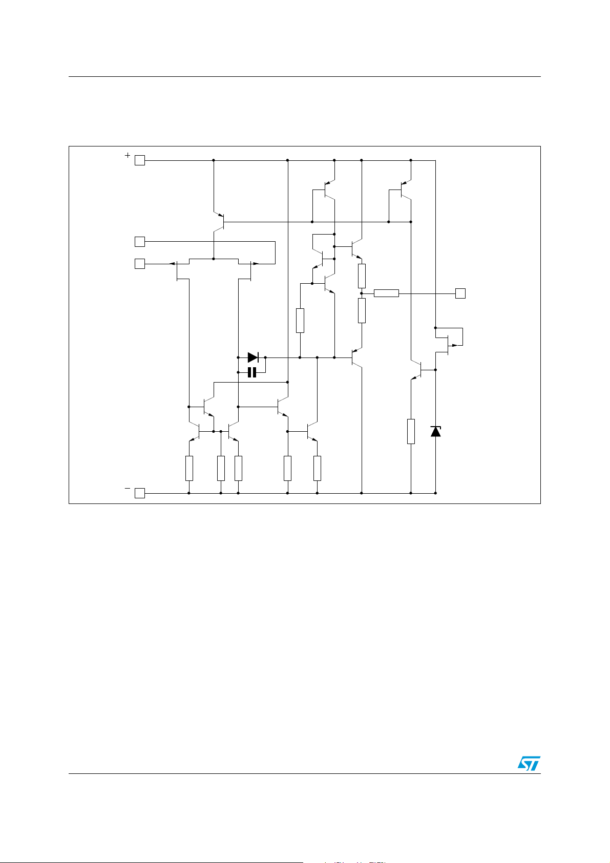
Schematic diagram TL072, TL072A, TL072B
Output
Non-inverting
input
Inverting
input
V
CC
V
CC
200
Ω
Ω
100
Ω
100
1.3k
1/2 TL072
30k
35k
35k
Ω
100
1.3k
8.2k
1 Schematic diagram
Figure 1. Schematic diagram
2/16 Doc ID 2298 Rev 7
TL072, TL072A, TL072B Absolute maximum ratings and operating conditions
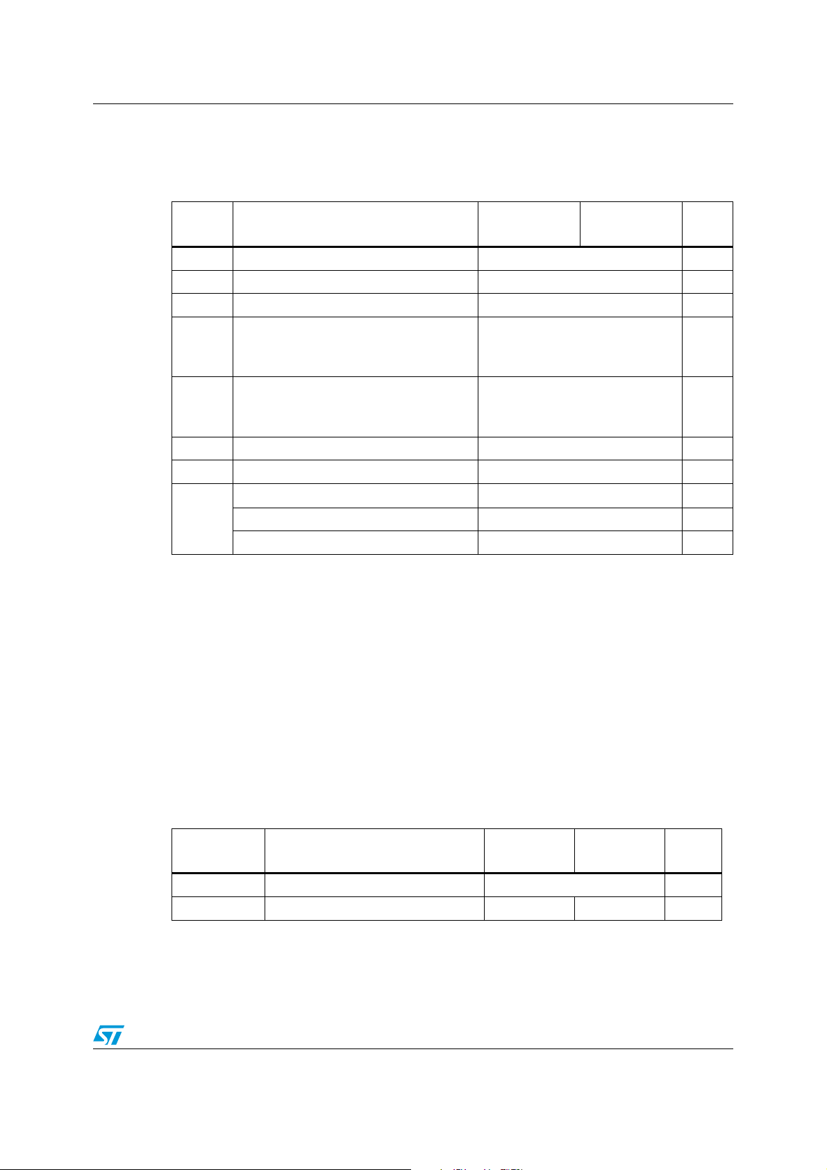
2 Absolute maximum ratings and operating conditions
Table 1. Absolute maximum ratings
Symbol Parameter TL072I, AI, BI
V
V
V
Supply voltage
CC
Input voltage
in
Differential input voltage
id
Thermal resistance junction to ambient
R
thja
SO-8
(1)
(2)
(3)
(4)
DIP8
Thermal resistance junction to case
R
thjc
SO-8
(4)
DIP8
Output short-circuit duration
T
Storage temperature range -65 to +150 °C
stg
HBM: human body model
ESD
MM: machine model
(7)
CDM: charged device model
1. All voltage values, except differential voltage, are with respect to the zero reference level (ground) of the
supply voltages where the zero reference level is the midpoint between V
2. The magnitude of the input voltage must never exceed the magnitude of the supply voltage or 15 volts,
whichever is less.
3. Differential voltages are the non-inverting input terminal with respect to the inverting input terminal.
4. Short-circuits can cause excessive heating. Destructive dissipation can result from simultaneous shortcircuits on all amplifiers.
5. The output may be shorted to ground or to either supply. Temperature and/or supply voltages must be
limited to ensure that the dissipation rating is not exceeded.
6. Human body model: 100 pF discharged through a 1.5 kΩ resistor between two pins of the device, done for
all couples of pin combinations with other pins floating.
7. Machine model: a 200 pF cap is charged to the specified voltage, then discharged directly between two
pins of the device with no external series resistor (internal resistor < 5 Ω). This is done for all couples of pin
combinations with other pins floating.
8. Charged device model: all pins plus package are charged together to the specified voltage and then
discharged directly to the ground.
(5)
(6)
(8)
CC
TL072C, AC,
BC
Unit
±18 V
±15 V
±30 V
125
°C/W
85
40
°C/W
41
Infinite
1kV
200 V
1.5 kV
+
and V
CC
-
.
Table 2. Operating conditions
Symbol Parameter TL072I, AI, BI
Supply voltage 6 to 36 V
Operating free-air temperature range -40 to +105 0 to +70 °C
T
V
CC
oper
Doc ID 2298 Rev 7 3/16
TL072C, AC,
BC
Unit
Electrical characteristics TL072, TL072A, TL072B
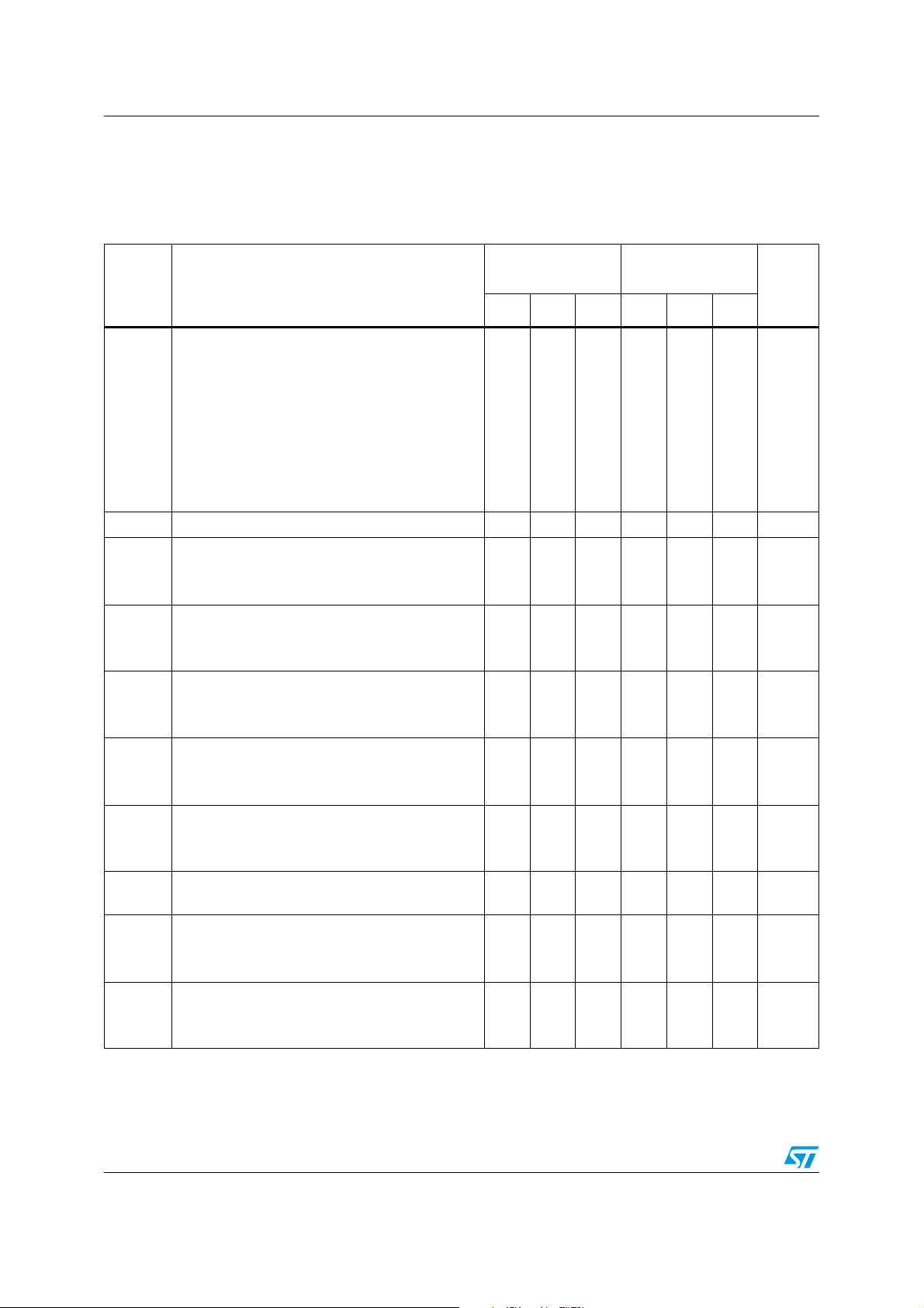
3 Electrical characteristics
Table 3. Electrical characteristics at VCC = ±15V, T
Symbol Parameter
Input offset voltage (Rs = 50Ω)
T
= +25°C
amb
TL072
TL072A
V
io
TL072B
T
min
≤ T
amb
≤ T
max
TL072
TL072A
TL072B
DV
Input offset voltage drift 10 10 µV/°C
io
≤ T
≤ T
(1)
max
(1)
max
Input offset current
I
io
T
T
Input bias current
I
ib
T
T
amb
min
amb
min
≤ T
≤ T
= +25°C
amb
= +25°C
amb
Large signal voltage gain (RL = 2kΩ, Vo = ±10V)
A
vd
SVR
T
= +25°C
amb
T
≤ T
amb
≤ T
max
min
Supply voltage rejection ratio (R
T
= +25°C
amb
T
≤ T
amb
≤ T
max
min
= 50Ω)
S
Supply current, no load
I
CC
V
icm
T
= +25°C
amb
T
≤ T
amb
≤ T
max
min
Input common mode voltage range
= +25°C (unless otherwise specified)
amb
TL072I,AC,AI
BC,BI
TL072C
Unit
Min. Typ. Max. Min. Typ. Max.
3
10
3
6
1
3
13
310
mV
13
7
5
5100
4
20 200
20
510010pA
20 200
20
nA
pA
nA
5025200 2515200 V/mV
808086 707086 dB
1.4 2.5
±11 -12 to
+15
2.5
±11 -12 to
1.4 2.5
2.5
+15
mA
V
CMR
Common mode rejection ratio (R
T
= +25°C
amb
T
≤ T
amb
≤ T
max
min
= 50Ω)
S
808086 707086 dB
Output short-circuit current
I
os
T
T
amb
min
= +25°C
≤ T
amb
≤ T
max
101040 606010
4/16 Doc ID 2298 Rev 7
10
40 60
60
mA
TL072, TL072A, TL072B Electrical characteristics
nV
Hz
------------
Table 3. Electrical characteristics at VCC = ±15V, T
(continued)
Symbol Parameter
Output voltage swing
T
= +25°C
amb
R
= 2kΩ
±V
SR
K
GBP
R
THD
e
opp
t
ov
r
i
n
L
R
= 10kΩ
L
T
≤ T
min
amb
≤ T
max
RL = 2kΩ
R
= 10kΩ
L
Slew rate
V
= 10V, RL = 2kΩ, CL = 100pF, unity gain
in
Rise time
V
= 20mV, RL = 2kΩ, CL = 100pF, unity gain 0.1 0.1
in
Overshoot
V
= 20mV, RL = 2kΩ, CL = 100pF, unity gain
in
Gain bandwidth product
V
= 10mV, RL = 2kΩ, CL = 100pF, F= 100kHz
in
Input resistance 10
Total harmonic distortion
F= 1kHz, R
=2V
V
o
= 2kΩ,CL = 100pF, Av = 20dB,
L
pp
Equivalent input noise voltage
RS = 100Ω, F= 1kHz
= +25°C (unless otherwise specified)
amb
TL072I,AC,AI
BC,BI
TL072C
Unit
Min. Typ. Max. Min. Typ. Max.
10
12
10
12
12
13.5
10
12
10
12
12
13.5 V
8 16 8 16 V/µs
µs
10 10 %
2.5 4 2.5 4 MHz
12
10
12
0.01 0.01
15 15
Ω
%
∅m Phase margin 45 45 degrees
V
o1/Vo2
1. The input bias currents are junction leakage currents which approximately double for every 10° C increase in the junction
temperature.
Channel separation
A
= 100
v
120 120 dB
Doc ID 2298 Rev 7 5/16
 Loading...